
Page 3
Advanced Epitaxy for Future Electronics, Optics,
and Quantum Physics
Rapid developments in semiconductor technology are occurring that are based on synthesis of thin layers and multilayered films of semiconductor crystals. These artificially layered materials can be grown in structures that confine and guide both light and electrons in special ways. They form microarchitectural materials of great precision and design flexibility. In this paper we describe the growth and the applications of these artificially structured epitaxial materials. We will examine the structures, how they are grown, and how they are being used for new light sources and high-speed electronics. We will then look at newly developed epitaxial structures, including quantum wires, quantum dots, and new materials for application to terahertz-frequency technology and nanometerscale microelectromechanical systems.
The growth techniques that are the most widely used and most fully developed for making multilayered epitaxial (i.e., crystalline) films are molecular beam epitaxy (MBE) and metal-organic chemical vapor deposition (MOCVD). Both techniques are capable of growing semiconductor films with thickness control and surface and interface smoothness with essentially atomic monolayer precision. In the case of MBE, crystals are formed by the delivery of neutral atoms in ultrahigh vacuum to the surface of the films [1]. The surfaces can be monitored during growth by electron diffraction so that surface smoothness and surface reconstruction are easily monitored. In MOCVD, gases react on a hot substrate to form the epitaxial films [2]. For both techniques, the smoothing of the surfaces can proceed at nearly an exponential rate. The smoothing is driven by a tendency of atoms to migrate on the surface and to stick at low spots, step edges, or depressions on the surface, where they can bind most strongly to the largest number of other atoms. The growth techniques were pioneered in the compound semiconductor families, especially the gallium arsenide III-V semiconductor family. Heteroepitaxy, in which a second material can be grown smoothly and without imperfection on an initial epitaxial film, was perfected initially in the GaAs/AlAs family and since then has been extended to many other systems. Differences in electron affinities between adjacent layers lead to a difference in potential energies for carriers in adjoining materials. This creates a potential step for both conduction electrons and holes. It is these potential steps in the conduction band and valence band edges that confine carriers and form the basis for band gap engineering [3]. The steps occur at the interfaces between the adjoining materials and can be very sharp. For an atomically abrupt interface, the potential steps are nearly atomically abrupt.
Page 4
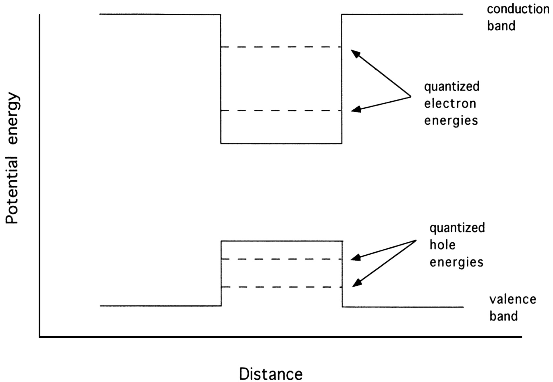
The potential wells formed by sandwiches of epitaxial semiconductor layers are illustrated in Figure 1. Quantization of the energy levels of the confined states of the electrons in the layers occurs as illustrated in the figure. Optical transitions between the confined electron energy states are allowed; consequently, electrons can emit photons as they drop from one energy level to another. Transitions from the lowest-conduction-band electron state to the highest-valence-band hole state produce the luminescence that is the basis of the light emission in quantum well lasers [4]. Today, quantum well lasers are the standard commercial semiconductor lasers and are used in applications as varied as fiber-optic communication; laser printing; materials processing; compact disc, CD-ROM, and digital video disc data storage; scientific instruments; optical pumping; medical treatment; and pointing and alignment. Recently developed quantum well lasers formed with gallium nitride epitaxy produce blue and white light previously impossible to produce with semiconductor devices. The greatly improved efficiency of semiconductor lasers and LEDs over traditional lightbulbs could revolutionize lighting [5]. Vertical-cavity, surface-emitting lasers (VCSELs) are a new generation of quantum well lasers that emit light from the surface of the epitaxial structures (as opposed to the edges). They can be formed into arrays of light emitters on a single chip with high efficiencies and low power usage.
In addition to enabling much of today's light wave technology, the flexible architecture and control of epitaxial growth are also powerful in allowing new, high-performance electronic devices and structures to be designed and fabricated. A particularly significant structure is the modulation-
~ enlarge ~
FIGURE 1 Potential wells for electrons and holes in epitaxial semiconductor sandwich. Wells are formed by layers of semiconductor materials with different electron affinities and band gaps. Lowest quantized electron energies and highest quantized hole energies are shown.
Page 5
doped heterostructure. In this structure, also known as a selectively doped or high-electron-mobility heterostructure, electrons and holes move in thin undoped channel layers that are adjacent to, but separate from, layers containing the donor or acceptor impurity atoms that provide carriers to the highly conducting channel. The separation of charge carriers from the dopant impurities reduces the collisions of the carriers with the impurities and leads to enormously enhanced carrier mobilities. Record electron mobilities of more than 20 million cm2/Vs have been achieved in these structures at low temperatures [6]. Although the electron mobilities are less at higher temperatures, where the electrons are scattered by lattice vibrations, the structures still provide major advantages in transistor design and performance. The modulation-doped, high-electron-mobility transistors are the most sensitive and efficient microwave and radio-frequency transistors. They have enabled increased operating frequencies and reduced receiver dish sizes in today's direct broadcast satellite systems. They are also in wide use in cellular telephones, where they provide greater sensitivity and reduced battery drain.
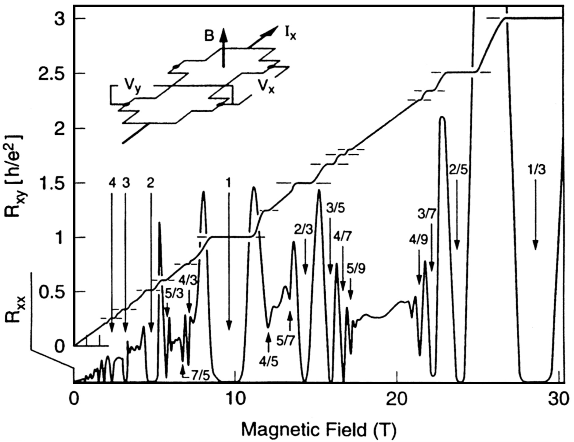
Modulation-doped heterostructures are also important in the study of the physics of electrons moving in two dimensions. The impact of modulation doping on the study of the physics of the two-dimensional electron gas derives from the relatively long time between carrier collisions in the high-mobility structures. This allows electrons to travel longer distances without collisions. Thus, in transverse magnetic fields, electrons can perform many orbital cyclotron revolutions before a scattering event. This allows clear observation of the quantization effects associated with cyclotron orbits and Landau levels (Figure 2). It makes possible an especially clear observation of the quantum Hall effect (in which the Hall resistance is quantized in units of h/e2). It also allowed the discovery of the fractional quantization of the Hall effect (in which the Hall resistance is quantized in fractions of h/e2) [7]. The fractional quantum Hall effect results from interactions among electrons at low temperatures in high magnetic fields, where all electrons in a two-dimensional electron gas lie in the lowest Landau level. The fractional states form an essentially new state of matter. The quantum Hall effect and the fractional quantum Hall effect were each the basis of a Nobel physics prize. Their chain of development illustrates an exceptionally fruitful interplay between device technology, advanced materials growth, and physics discovery.
With two-dimensional epitaxial structures having made strong impacts on devices and physics, it is natural to examine structures where the electrons are constrained to only one or zero degrees of freedom. One way to approach these lower-dimensional structures is by modification of a two-dimensional electron structure by surface gates or by etching. Small channels and confining regions can be formed so that the electron motion can be suitably constrained. Notable success has come from fabrication of small metallic electrical gates just above a selectively doped high-mobility, two-dimensional electron gas. In such gated structures, electrons can be guided through small constrictions (referred to as quantum point contacts) in which the electron conductance is quantized in integral multiples of e2/h. The gates can also be arranged in shapes to create quantum dots in which electron motion in all directions is quantized (Figure 3). The quantized accumulation of charge within the dots can be observed in the so-called Coulomb blockade [8], and quantized motion of charge can be seen in the so-called quantum turnstile. An adiabatic quantum pump has recently been demonstrated in which electric current is produced by cyclic deformation of the confining potential of an open quantum dot [9].
As mentioned above, the formation of almost atomically smooth surfaces and interfaces in epitaxial growth is driven by the motion of adatoms on surfaces to stable incorporation sites. This provides a strong driving force for the formation of smooth surfaces. The lithographic processing of the surfaces that we have just discussed has been a powerful way to make quantum wires and quantum boxes (also known as quantum dots), but it is limited by size limits of lithography. Dimensions below
Page 6
~ enlarge ~
FIGURE 2 Quantum Hall effect and fractional quantum Hall effect in a two-dimensional electron gas in GaAs at T = 85 mK. The Hall resistance Rxy = Vy/Ix and the magnetoresistance Rxx = Vx/Ix are shown. Plateaus in Rxy and valleys in Rxx occur at integral and fractional values of the filling of the cyclotron (Landau) levels. Reprinted by permission from Stormer, H.L., D.C. Tsui, and A.C.Gossard. The fractional quantum Hall effect. Reviews of Modern Physics, Feb. 1999, vol.71 (no.2):S298-S305. Copyright 1999 by the American Physical Society.
0.1 micrometer become exceedingly difficult to achieve and control with lithographic processing. This makes it desirable to look for ways to produce spontaneous formation of wires, boxes, or rods in the crystal growth process. By solution chemistry, very small spherical particles that are effectively quantum dots or quantum boxes can be formed. Means to make rodlike particles by similar solution chemistry techniques are now being discovered [10].
In semiconductor epitaxy, growth techniques are also being developed to produce self-organized quantum dot and quantum wire structures. As an example of lateral self-organized growth of quantum structures, growth on an atomically stepped or terraced crystal surface provides a means of defining lines of atoms. The terraced surfaces can be produced by cutting a substrate wafer from a bulk crystal at a slight angle relative to the principal crystal axes of the bulk crystal. Epitaxial growth on such a surface typically proceeds by migration of the adatoms across the crystal terraces to incorporate at the step edges that occur between the terraces. Deposition of a submonolayer coverage of adatoms then produces atom-thick stripes of material that are distributed over the terrace edges. Alternately depositing different materials where the total coverage of each pair of depositions is an integral multiple or fraction of a monolayer then leads to a coherent alignment of the stripes in successive
Page 7
Figure 3 may be viewed in the print version of this report. The original figure appeared in Livermore, C., C.H. Crouch, R.M. Westervelt, K.L. Campman, and A.C. Gossard, “The Coulomb Blockade in Coupled Quantum Dots,” Science, November 22, 1996, Vol. 274, pp. 1332-1335, copyright 1996 by the American Association for the Advancement of Science, Washington, D.C.
Page 8
layers. The resultant epitaxial structure is an array, or superlattice, of quantum wires [11]. The periodicity of the superlattice is determined by the spacing between the terrace steps. The limits on the perfection of the quantum wire superlattices are the nonuniformity of the terrace step spacing, kinks in the terrace steps, and possible interdiffusion during growth.
When epitaxial structures are grown in which a material with a somewhat different crystal lattice spacing is grown on an original material, another kind of self-ordering can occur that provides an effective way to make quantum dots. In this case, adatoms with larger radii than the substrate atoms can relieve their compressive strain by forming islands in which they can spread out. This layer/island growth mode (known as Stranski-Krastanow growth) enables InAs depositions on GaAs substrates to organize themselves into islands [12]. InAs has a lattice constant that is 7 percent larger than GaAs. The islands are quantum dots whose sizes can be just a few nanometers. This is far smaller than can yet be achieved by lithography. Furthermore, the islands can be embedded by an overgrowth process. Then the process can be repeated to make stacked layers of these self-assembled quantum dots. The self-assembled quantum dot islands can be grown by both MBE and MOCVD. They form the basis for a rich and active pursuit of the science and technology of quantum dots. The localization of charge that they produce within semiconductor lasers can be beneficial to laser operation. Quantum dot lasers have been made with these materials, and it is believed that quantum dot confinement may be playing a major role in the successful operation of blue gallium nitride lasers, which typically contain InGaN active layers [13]. Electrical charging of the dots, one electron at a time, can be observed. Quantum-confined luminescence from the quantum states of the dots can also be seen. The major limitations on the dot structures are nonuniformity in their shape, size, spacing, and arrangement. Each of these issues is critically dependent on growth technique and technology. The ultimate impact of quantum dots on science and technology will depend strongly on the resolution of these issues.
In addition to quantum structures in semiconductors, it is interesting and useful to form metal/semiconductor composite nanostructures. A path to such structures has been provided by low-temperature epitaxy of compound semiconductors. It was discovered that epitaxial growth of crystalline GaAs could be performed at lower than conventional growth temperatures, with the result that excess As could be incorporated in the growth [14]. GaAs can be grown epitaxially at temperatures down to 200 °C, compared to more conventional growth temperatures of 500 °C to 700 °C. With an appropriate excess flux of arsenic relative to gallium, 1 to 2 percent of excess arsenic (relative to exactly stoichiometric GaAs) can be incorporated with low temperature growth. The excess arsenic provides electron traps (deep impurity states that pin the Fermi level in the gap of the GaAs), producing high-resistivity material and rapid recombination of electrons and holes. Annealing the material leads to diffusion of the excess arsenic to form metallic arsenic nanoparticles with diameter approximately 10 nanometers. The composite GaAs-As semiconductor-metal material can be applied to growing nonconductive insulation layers for application in field effect transistors to isolate semi-insulating substrates from transistor channel layers. The deep trap states and the metal particles in low-temperature-grown GaAs also provide efficient trapping of photo-induced carriers and rapid recombination of photo-induced electrons and holes. They are attractive for making fast photodetectors and phototransistors, eliminating long-lived carriers that would slow response and add dark current [15].
A significant application of low-temperature-grown GaAs has been the production of fast photoconductive materials for use in generation of terahertz-frequency electromagnetic waves [16]. The low-temperature-grown GaAs is the active element in photoconductive structures that generate electromagnetic radiation at the difference frequency between laser pumping beams that are striking the material. These photomixers produce levels and coherence of far-infrared terahertz-frequency radiation that can be the basis of a semiconductor far-infrared terahertz technology. These radiation sources are needed in astrophysics for the sensitive heterodyne detection of radiation from gases
Page 9
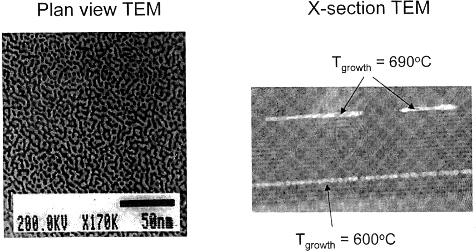
involved in star and galaxy formation as well as for detection of radiation from gases in Earth's atmosphere. Photoconductive mixers based on the low-temperature-grown GaAs and pumped by semiconductor lasers are providing highly coherent tunable CW radiation at record power levels in the terahertz frequency regime. This is particularly significant because of the absence of other viable semiconductor technologies for sources in the terahertz frequency region. Sources employing metallic nanoparticle composites of erbium arsenide (ErAs) particles in GaAs are now also showing promising performance in this application (Figure 4) [17]. The ErAs particles are formed by MBE codeposition of Er with GaAs and provide an alternate and highly engineerable approach to metal/semiconductor composites and high-speed photoconductors.
Yet another important functionality being provided by advanced epitaxial growth is the creation of magnetic semiconductors [18]. By inclusion of a sufficient concentration of magnetic atoms within a semiconductor, it is possible to produce magnetically ordered semiconductors. Extensive work has been performed on magnetic II-VI compound semiconductors such as CdMnTe. More recently, magnetic semiconductor alloys of GaMnAs have been grown with ferromagnetic Curie temperatures above 100 K in materials containing about 5 percent manganese. This raises the interesting possibility of “spintronics” and quantum computation technologies, in which information is stored and transmitted in semiconductors both as charge and as spin.
Still another emerging application of epitaxial semiconductors is in microelectromechanical systems (MEMS) and the smaller nanoelectromechanical systems (NEMS). Thin epitaxial layers that are remarkably flexible can be grown and subsequently released from their substrates by selective etching. This allows the formation of flexible, nearly perfect crystalline layers for MEMS or NEMS application. Free-standing films forming compliant cantilevers of thickness less than 100 nanometers
~ enlarge ~
FIGURE 4 (left) Plan view transmission electron microscope (TEM) image of metallic ErAs islands in GaAs:ErAs semiconductor/metal epitaxial composite material. SOURCE: Kadow, C., J.A. Johnson, K. Kolstad, J.P. Ibbetson, and A.C. Gossard. Growth and micro structure of self-assembled ErAs islands in GaAs. Journal of Vacuum Science and Technology B, 2000, vol. 18 (no. 4):2199. (right) Cross-sectional TEM image of ErAs islands grown at Tgrowth = 690 °C and 600 °C. SOURCE: Schmidt, D.R., J.P. Ibbetson, D.E. Brehmer, D.J. Palmstrom, and S.J. Allen. Giant magnetoresistance of self-assembled ErAs islands in GaAs. Materials Research Society Symposium Proceedings, 1997, vol. 475:252.
Page 10
have been fabricated. They provide sensitive elements for magnetic force magnetometry. The first measurements on these are showing sensitivities that are close to those of SQUID magnetometers [19].
When cantilevers are grown that contain modulation-doped, high-mobility electron layers near the surface, we have a way to incorporate field-effect transistors within the cantilevers. These field-effect transistors within the cantilever provide an ultrasensitive way to sense deflections of the cantilever. The cantilever deflections produce changes in electron density within the channel because of the strain-dependence of their electrical conductivity and because of piezoelectric effects that polarize the material when it is bent. When the surface of an appropriately oriented GaAs cantilever stretches, an electric field perpendicular to the surface develops. This field is produced by the piezoelectric effect and results from the relative motion of anions and cations with respect to each other in response to the strain. The field can accumulate or deplete electrons beneath a surface gate and thus turn on or off the field effect transistor. These self-sensing cantilevers show sensitivity comparable to the more conventional cantilever arrangements based on deflection of a laser beam reflected from the cantilever surface that are presently used in most atomic force microscopes [ 20]. But the self-sensing cantilevers offer considerably more potential for integration of arrays of cantilevers.
The structures and the applications that we have discussed here have given some idea of the development and uses of multilayered epitaxial thin films. In summary, the advanced epitaxial growth of semiconductor materials has repeatedly enabled interesting intersections between basic science and applied technology. The areas of science and technology that encompass new materials, new science, and new devices are enabled by the new epitaxial materials and give every indication of continued fruitfulness.
NOTES
1. Herman, Marian A., and Helmut Sitter. Molecular Beam Epitaxy: Fundamentals and Current Status, 2nd Edition, Springer Series in Materials Science 7, New York (Springer-Verlag New York, 1996).
2. Stringfellow, Gerald B. Organo-metallic Vapor Phase Epitaxy: Theory and Practice, 2nd Edition, San Diego, Calif. (Academic Press, 1999).
3. Davies, John H. The Physics of Low-dimensional Semiconductors: An Introduction, New York (Cambridge University Press, 1998).
4. Coldren, Larry A., and Scott W. Corzine. Diode Lasers and Photonic Integrated Circuits, New York (John Wiley and Sons, Inc., 1995).
5. Nakamura, S. InGaN-based violet laser diodes. Semiconductor Science and Technology, June 1999, vol. 14 (no. 6):R27-R40.
6. Kane, B.E., L.N. Pfeiffer, and K.W. West. High mobility GaAs heterostructure field effect transistor for nanofabrication in which dopant-induced disorder is eliminated. Applied Physics Letters, 28 Aug. 1995, vol. 67 (no. 9): 1262-1264.
7. Stormer, H.L., D.C. Tsui, and A.C. Gossard. The fractional quantum Hall effect. Reviews of Modern Physics, Feb. 1999, vol. 71 (no. 2):S298-S305.
8. Livermore, C., C.H. Crouch, R.M. Westervelt, K.L. Campman, and A.C. Gossard. The Coulomb blockade in coupled quantum dots. Science, 22 Nov. 1996, vol. 274 (no. 5291): 1332-1335.
9. Switkes, M., C.M. Marcus, K.L. Campman, and A.C. Gossard. An adiabatic quantum electron pump. Science, 19 March 1999, vol. 283 (no. 5409): 1905-1908.
10. Wickham, J.N., A.B. Herhold, and A.P. Alivisatos. Shape change as an indicator of mechanism in the high-pressure structural transformations of CdSe nanocrystals. Physical Review Letters, 31 Jan. 2000, vol. 84 (no. 5):923-926.
11. Swiatek, K., H. Weman, M.S. Miller, P.M. Petroff, and J.L. Merz. Investigation of interface quality in (Al,Ga )As serpentine superlattice quantum wires by microwave modulation of exciton luminescence. Electron Technology, 1996, vol. 29 (no. 2-3):305-308.
Page 11
12. Romanov, A.E., P.M. Petroff, and J.S. Speck. Lateral ordering of quantum dots by periodic subsurface stressors. Applied Physics Letters, 19 April 1999, vol. 74 (no. 16):2280-2282.
13. Zhukov, A.E., A.R. Kovsh, V.M. Ustinov, Y.N. Shernyakov, S.S. Mikhrin, N.A. Maleev, E.Y. Kondrat'eva, D.A. Livshits, M.V. Maximov, B.V. Volovik, D.A. Bedarev, Y.G. Musikhin, N.N. Ledentsov, P.S. Kop'ev, Z.I. Alferov, and D. Blimberg. Continuous-wave operation of long-wavelength quantum-dot diode laser on a GaAs substrate. IEEE Photonics Technology Letters, Nov. 1999, vol. 11 (no. 11):1345-1347.
14. Kisielowski, C., A.R. Calawa, and Z. Liliental-Weber. The effect of excess gallium vacancies in low-temperature GaAs/AlAs/GaAs:Si heterostructures. Journal of Applied Physics, 1 July 1996, vol. 80 (no. 1):156-160.
15. Melloch, M.R., D.D. Nolte, J.M. Woodall, J.C.P. Chang, D.B. Janes, and E.S. Harmon. Molecular beam epitaxy of nonstoichiometric semiconductors and multiphase material systems. Critical Reviews in Solid State and Materials Sciences, 1996, vol. 21 (no. 3):189-263.
16. Verghese, S., K.A. McIntosh, and E.R. Brown. Highly tunable fiber-coupled photomixers with coherent terahertz output power. IEEE Transactions on Microwave Theory and Techniques, Aug. 1997, vol. 45 (no. 8, pt. 2):1301-1309.
17. Kadow, C., A.W. Jackson, A.C. Gossard, J.E. Bowers, S. Matsura, and G.A. Blake. Self-assembled ErAs islands in GaAs for THz applications. Physica E, April 2000, vol. 7 (no. 1-2):97-100.
18. Ohno, H. Ferromagnetism and heterostructures of III-V magnetic semiconductors. (Proceedings of 13th International Conference on the Electronic Properties of Two-Dimensional Systems, Ottawa, Ont., Canada, 1-6 Aug. 1999). Physica E, Feb. 2000, vol. 6 (no. 1-4):702-708.
19. Harris, J.G.E., D.D. Awschalom, F. Matsukura, H. Ohno, K.D. Maranowski, and A.C. Gossard. Integrated micromechanical cantilever magnetometry of Ga1−xMnxAs. Applied Physics Letters, 23 Aug. 1999, vol. 75 (no. 8):1140-1142.
20. Beck, R.G., M.A. Eriksson, M.A. Topinka, R.M. Westervelt, K.D. Maranowski, and A.C. Gossard. GaAs/AlGaAs self-sensing cantilevers for low temperature scanning probe microscopy. Applied Physics Letters, 24 Aug. 1998, vol. 73 (no. 8):1149-1151.


