
Page 83
From Clusters to Automobiles: Processing and Applications of Granular Nanomaterials
HORST W. HAHN
Institute of Materials Science Darmstadt University of Technology Darmstadt, Germany
Matter with nanometer-size structures has been around for billions of years in the universe. It is currently speculated that the assembly of nanometer-size particles into larger building blocks that eventually exhibit gravitational forces is the basic mechanism of planet formation in the proximity of newly formed stars. On Earth, scientists have been attracted to clusters consisting of a few to a few hundred atoms because of the interesting physical and chemical properties that are dominated by quantum-size effects. More than 15 years ago, a new field of materials science evolved, initiated by the original work of Gleiter (1989), and is now an integral part of the broader field of nanotechnology. This new field is based on the fact that many properties of materials with technological relevance depend on the size of the microstructural features, such as grain size, or are influenced by the large fraction of interfaces that exhibit a disordered structure compared to the usual crystalline order. The detailed description of the internal structure of a material is commonly termed “microstructure.”
Here I present the potential of manmade materials with microstructural features in the nanometer range, along with a few examples of technological relevance. In general, nanomaterials can exhibit nanometer-size features in zero, one, two, and three dimensions. Consequently, these materials are named “clusters/nanoparticles,” “multilayers,” “thin films,” and “nanocrystalline materials.” Their common feature is that the fraction of atoms residing in the interfacial regions, such as surfaces and grain/phase boundaries, is extremely large and can exceed 50 percent of the total number of atoms for dimensions in the order of 5 nm. In order to tailor the physical and chemical properties of nanomaterials, the microstructure has to be controlled on the level of a few nanometers or even on the atomic level, during the entire synthesis and processing. Presented here are
Page 84
gas phase techniques that allow the synthesis of all nanostructured materials irrespective of their dimensionality. Examples of size-dependent properties and their technological applications are given. The materials are not limited to clusters, nor are the applications restricted to automobiles, but include all classes of nanostructured materials mentioned above and apply as well to such application areas as UV protection, catalysis, hard disks, magnetoelectronic devices, and many more, demonstrating the enormous potential of the design of materials on the nanometer scale.
Gas phase processes provide a convenient and versatile way to prepare materials, with excellent control of the microstructure starting from an atomic level. Techniques such as sputtering, Molecular Beam Epitaxy (MBE), and Chemical Vapor Deposition (CVD) are well-established processes, even in industrial production of thin-film devices. The underlying principle is the transfer of atoms/ molecules into the gas phase and their deposition onto an appropriate substrate, where the growth is controlled on the atomic level by adjusting temperature, growth rates, and so forth. By employing sophisticated technological modifications of the basic principles, thin films, multilayered structures, and granular materials—that is, nanoparticles embedded in a matrix—can be readily prepared. Simply increasing the gas pressure in the synthesis chamber from the range of the above processes (10−11to 10−3mbar) to the range from 1 mbar to ambient pressure, and/or increasing the precursor partial pressures, changes the growth mechanisms drastically, and a whole new class of nanomaterials can be obtained. Because of the elevated pressure, clusters/nanoparticles are nucleated in the gas phase by the increase of collisions between the precursor atoms or molecules. Consequently, the processes are termed (Inert) Gas Condensation (IGC) and Chemical Vapor Synthesis (CVS), referring to the difference of the growth mechanisms.
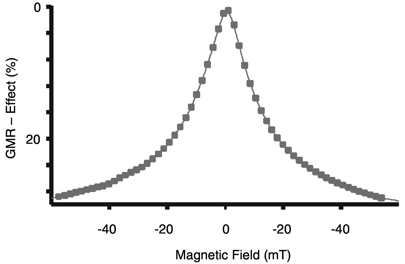
Recently, it was discovered that the electrical resistivity of a multilayered structure consisting of alternating layers of a ferromagnetic metal, such as Co, and a nonferromagnetic metal interlayer, such as Cu, is drastically reduced in a magnetic field. The effect was termed Giant Magnetoresistance (GMR), because of the large change of the resistance of up to 100 percent, compared to the much smaller Anisotropic Magnetoresistance (AMR) effect. Besides the interest in gaining a basic understanding of the physical concepts of GMR, the main driver for the immense efforts in the field of magnetoresistance effects has been the potential for applications in electronic data storage and for a large variety of precision sensors for revolutions and angle detection.
A structural prerequisite for the GMR effect is the exact control of the thickness of the interlayers in the range of 1 to 2 nm, that is, 5 to 10 monolayers. Depending on the thickness of the interlayer, either ferromagnetic or antiferromagnetic coupling between the two neighboring magnetic layers is observed. In the case of antiferromagnetic coupling, a magnetic field can change the direction of the magnetic moments of some layers, resulting in the observed decrease of
Page 85
~ enlarge ~
FIGURE 1 Change of the normalized electrical resistance (GMR effect) as a function of the magnetic field for a granular thin film of silver/cobalt prepared by molecular beam epitaxy. SOURCE: Alof, 2000.
the resistance. The change of the resistance as a function of the applied magnetic field is shown in Figure 1.
After the initial discovery of the GMR effect, other structures exhibiting insulating interlayers instead of the nonferromagnetic metals and spin valves with only a few nonperiodic layers have shown comparable resistance effects. The first case results in the Tunneling Magnetoresistance (TMR) effect, which has a tremendous potential for applications in nonvolatile data storage devices. Additionally, granular structures consisting of nanometer-size particles embedded in a metallic matrix have been examined because of the much simpler production and their increased stability at elevated temperatures. In this case, two metals, such as cobalt and silver, with no or little solubility, are codeposited onto heated substrates using sputtering or MBE techniques. The major disadvantage of granular structures is the large magnetic field required to obtain an effect. By optimization of the size, shape, and distribution of the nanoparticles in the matrix, the material can be used for sensor applications—in particular, for high temperature capabilities (Alof, 2000). In the system silver-iron, it was shown by comparison of the fraction of Fe atoms in the interfaces to the Ag matrix determined by Mössbauer spectroscopy with the observed GMR effect that the interfaces play a crucial role for the magnetoresistance effect (Alof et al., 2000). These measurements demonstrate the importance of the interfacial regions that
Page 86
~ enlarge ~
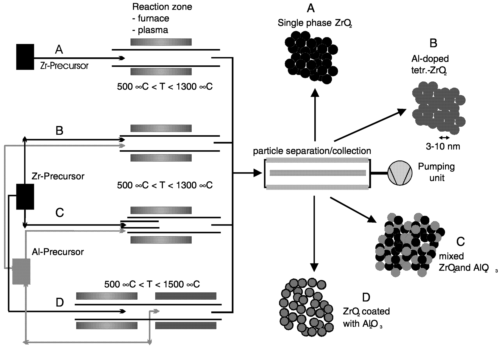
FIGURE 2 Schematic of the different opportunities of Chemical Vapor Synthesis for the preparation of nanocrystalline powders of ZrO2and in the system ZrO2/Al2O3,with different elemental distribution. SOURCE: Hahn, private communication.
Page 87
~ enlarge ~
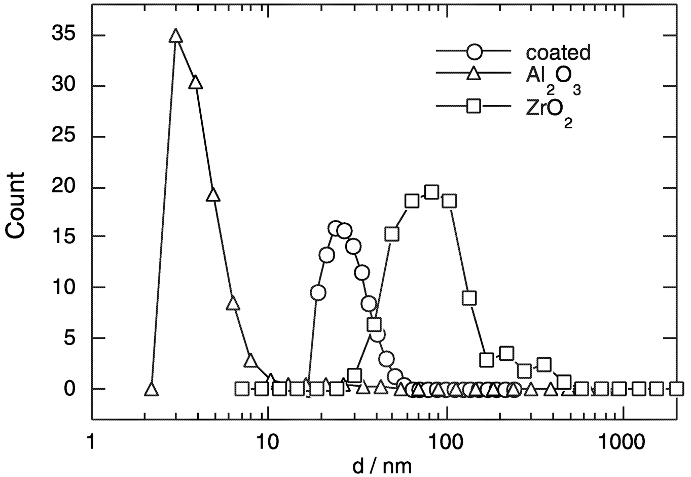
FIGURE 3 Size distribution of dispersions of the pure oxides ZrO2and Al2O3 in water. Note the improvement of the size distribution of ZrO2coated with a thin layer of Al2O3. The alumina nanoparticles can be dispersed to the size of the dry as prepared powder. SOURCE: Möller, 2000.
dominate in nanostructured materials and the control of structures and composition on a nanometer scale.
Nanoparticles synthesized by gas phase processes (IGC and CVS) can be used as prepared, after surface functionalization or after further processing, such as compaction and sintering, depending on the properties of interest. Examples are catalytic properties, gas sensing properties, enhanced sintering (Srdic et al., 2000), and superplasticity (Betz et al., 1997). While in zero-dimensional structures the drastic increase of the specific surface area as well as the details of the atomistic surface structure are important, three-dimensional structures are of interest because of the large fraction of internal interfaces that enhance grain-sizedependent properties. In Figure 2the opportunities of the CVS method are schematically shown for the case of oxide nanoparticles consisting of several cations. The different elemental distribution (doped nanoparticles, binary mixtures on the nanometer scale of two different oxide nanoparticles, and coated/ surface functionalized nanoparticles), which can be readily prepared using CVS, results in different properties at the same nominal composition. The effect of surface modification can be seen in Figure 3for the dispersion behavior of ZrO2, Al2O3, and Al2O3-coated ZrO2in water without the use of surfactants. The
Page 88
dispersion behavior is different for the different oxides, which is due to the surface charge, and can be adjusted by the surface composition even on the level of submonolayers. The total force between individual nanoparticles can be calculated theoretically by considering the various attractive and repulsive interaction forces. From the calculation it is determined that ZrO2nanoparticles will agglomerate into larger particles, whereas Al2O3 nanoparticles will exhibit a total repulsive force. As can be seen from Figure 3, the experimental particle size distribution for Al2O3 confirms the theoretical calculation. The predictability of the dispersion behavior is essential in many industrial processes involving dilute and concentrated particle dispersion in solvents.
REFERENCES
2000. GMR-Efekt in granularen metallischen Schichten für Sensoranwendungen. Ph.D. dissertation. Technische Universität Darmstadt, VDI Fortschritt-Berichte, Reihe 9, Nr. 326, 1–150.
, , , and . 2000. Interface contribution to giant magnetoresistance in granular AgFe studied with Mössbauer spectroscopy. Journal of Applied Physics 88(7): 4212–4215.
, , , and . 1997. Low-temperature deformation behavior of nanocrystalline 5 mol% yttria stabilized zirconia under tensile stresses. Nanostructured Materials 8: 845–853.
1989. Nanocrystalline materials. Progress in Materials Science 33: 223–315.
2000. Modellierung der Dispergierbarkeit nanokristalliner Al2O3- und TiO2-Pulver. Ph.D. dissertation. Technische Universität Darmstadt.
, , and . 2000. Sintering behavior of nanocrystalline zirconia doped with alumina prepared by chemical vapor synthesis. Journal of the American Ceramic Society 83(8): 1853–1860.


