
Page 93
Nanoscale Materials: Synthesis, Analysis, and Applications
RUDOLF M. TROMP
IBM T. J. Watson Research Center Yorktown Heights, New York
ABSTRACT
With the national initiative on nanotechnology, the art and science of the nanoworld have broken out of the lab and into the limelight of the media as well as the consciousness of politicians, business leaders, and the lay public. As in many nascent areas of science and technology, research advances in the lab are heralded as major breakthroughs promising faster computers, cheaper technologies, and better lives. But before concerning ourselves with the wonderful things that nanotechnology will do, we should look at some of the nanomaterials that will be at the bottom of this “food chain.” What is the stuff of the nanoworld? How do we make it, how do we look at it, and, then, what might we do with it? Here, I touch on some of the broader issues and then focus on a particular example: the self-assembly of quantum dots and nanocrystals, the study of their evolution and structure, and their possible use in a variety of technologies.
As technologies continue to scale to ever-smaller dimensions, with 100-nm features in sight in semiconductor technology (Packan, 1999), excitement about materials on the nanoscale is heating up. In semiconductor technology, for example, scaling has been the driving force of the industry for decades. But it now appears that several fundamental barriers will limit scaling. Gate oxides are approaching a thickness of a mere 2 nm, where quantum mechanical tunneling becomes a serious concern because of its negative effect on device lifetime. The number of dopant atoms in the active region of a transistor becomes so small that statistical variations become significant, giving rise to undesirable device-to-device variations in operation. Also, it becomes increasingly hard to make such small devices because of the intrinsic resolution limits of traditional optical li-
Page 94
thography, even with wavelengths pushing well into the ultraviolet. Similarly, the size of a magnetic bit on a storage disk is rapidly approaching the so-called paramagnetic limit, where thermal fluctuations destabilize the stored information, and reliable long-term storage becomes impossible. This hardly means that we are approaching the end of the computer revolution, but the material under-pinnings of this revolution may be ready for a revolution of their own.
Some materials experts are undeterred by the limits of scaling. If scaling no longer works, the nanometer world has properties and promises of its own that go beyond scaling and that may create entirely new technologies based on new physics, materials, and paradigms. If this nanometer world is too small to be assembled by man, then let it assemble itself—a practice long known, practiced, and treasured by chemists and biologists. Clouds have a certain range of temperatures and contain a certain amount of water vapor. Under the right conditions, snowflakes, wonderfully intricate ice crystals, come falling out. They were not put together by anyone: they self-assembled. The worldwide drive to invest in and develop “nanotechnology” reflects the optimism that such a technology will soon become reality and that it will spawn new capabilities, opportunities, and wealth.
It may be useful to ask which structures on the nanoscale display what new phenomena and where these may be used in present or future technologies. For instance, what are “quantum dots,” what properties do they have, and how can they be useful in creating new devices (Materials Research Society, 1998)? How do we make them? What level of control do we have, and what level do we need? How do we even look at them? This approach works from an evolving body of materials knowledge and involves looking for new ways to apply this knowledge. It relies on the assumption that if we know enough, applications will offer themselves almost unavoidably.
Alternatively, the general structure and properties of quantum mechanics have been explored to establish the new field of quantum cryptography and quantum computing (DiVincenzo, 1995). “Consider the superposition of two quantum states,” a typical paper may state. What does this correspond with in the material world? How do we create such a superposition, and how do we manipulate it? Is this quantum world a nanoworld (atoms or quantum dots; Loss and DiVincenzo, 1998) or a more familiar microworld (superconductivity; Mooij et al., 1999). Does it matter which? Is the microworld a convenient testbed for the near future and the nanoworld the goal for a more remote future? Here the application is well defined, but the material basis is not. Quantum computers would do certain tasks much faster than digital computers. Will nanotechnology make practical quantum computing a reality?
There may be some discussion as to what nanotechnology actually is. For the present time it may be most useful to consider it the science of things on the nanoscale—anywhere from Angstroms to tenths of micrometers, which includes large chunks of materials science, physics, chemistry, and biology. Here, I look
Page 95
at the science of quantum dots—a good example of small structures formed by self-assembly.
QUANTUM DOT SELF-ASSEMBLY
There are at least two very different ways to make quantum dots assemble themselves. The first method (Nishi et al., 1996) consists of exposing a surface to a flux of foreign atoms or molecules: Take an atomically clean silicon (Si) surface and expose it to a vapor of germanium (Ge) atoms. The Ge atoms will at first wet the Si surface, growing a thin Ge layer over the Si wafer. However, Ge atoms are about 4 percent larger than Si atoms, giving rise to a misfit strain in this thin layer. After a thickness of three atomic layers has been reached, this misfit strain becomes too large, and any additional Ge atoms will aggregate in small, three-dimensional clusters. These Ge clusters or dots are so small—only 10 nm or so—that quantum mechanical effects play a significant role in their properties. Hence the name “quantum dots.” This method works not only for Ge on Si but for a broad range of elements and alloys, both semiconducting and metallic.
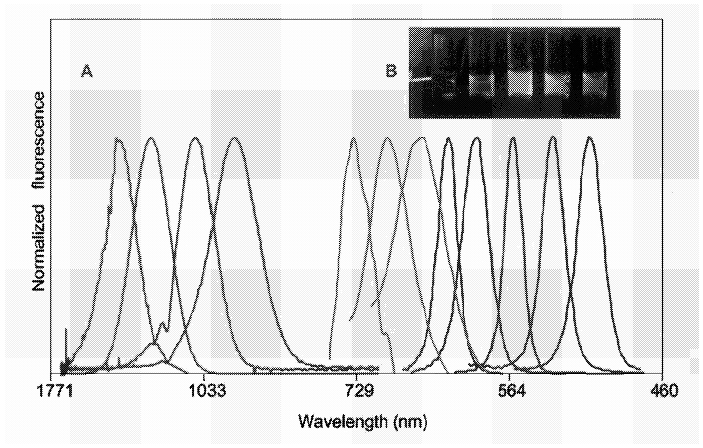
The other approach involves using wet chemistry (Murray et al., 2000): Take a beaker and dissolve one constituent in a suitable solvent, then rapidly add a second constituent so that a new phase can nucleate in the now supersaturated liquid. This makes it possible to fabricate, for example, CdSe quantum dots in macroscopic quantities. After nucleation the quantum dots can be left to “ripen” for some time. In the ripening process the average dot size increases with time. This can be compared with the condensation of steam onto a cold surface. Initially, the condensed droplets are small but with time the droplets increase in size, even if no more steam condenses. This is because larger dots or droplets have less surface area per volume and are therefore energetically favored. The ripening process allows a certain degree of control over the average dot size. In the case of quantum dot growth in a liquid, a separate “distillation” step allows particles to be selected with excellent size control. Different sizes have different properties. Figure 1 shows fluorescence data (Bruchez et al., 1998) from compound semiconductor quantum dots over a range of sizes, showing a continuous shift of fluoresence wavelength with size and increasing to longer wavelengths for larger size as expected.
Although size selection and control are relatively straightforward in the wet chemistry approach, things are not so simple on surfaces. One problem is that there is no equivalent to the size distillation step that worked so well for the CdSe quantum dots shown above. Second, nucleation can occur over a relatively long time window, giving rise to broad size distributions. Both growth methods have their own advantages, which makes each more suitable for specific purposes. If one wants to put quantum dots in a solid-state device, such as a laser or a memory element, then growth on a solid surface is convenient, since it
Page 96
~ enlarge ~
FIGURE 1 (a) Size- and material-dependent emission spectra of semiconductor nanocrystals. Blue: CdSe (diameters of 2.1, 2.4, 3.1, 3.6, and 4.6 nm, from right to left). Green: InP ( 3.0, 3.5, and 4.6 nm ). Red: InAs (2.8, 3.6, 4.6, and 6.0 nm). (b) True-color image of silica-coated core (CdSe)-shell (ZnS or CdS) nanocrystal probes in aqueous buffer, illuminated with an ultraviolet lamp. This figure can be viewed in color by accessing http://www.cchem.berkeley.edu/~pagrp/publications.html(Bruchez et al.). SOURCE: Reprinted with permission from Bruchez et al. Copyright 1998 American Association for the Advancement of Science.
allows for direct integration of quantum dot growth in the device manufacturing process. However, one cannot, in general, remove these dots from the substrate on which they were grown and utilize them elsewhere. Wet chemistry methods allow for the growth of large quantities of quantum dots that can easily be “carried around” and used in a wide diversity of applications.
Other methods to create nanocrystals include physical vapor synthesis (in which a supersaturated vapor is seeded into a cold gas to nucleate nanocrystals), arc discharge methods (very effective in making buckyballs), and protein-mediated self-assembly methods, among others. Here I focus on wet chemistry methods and vapor deposition onto a surface.
HOW TO LOOK AT QUANTUM DOTS
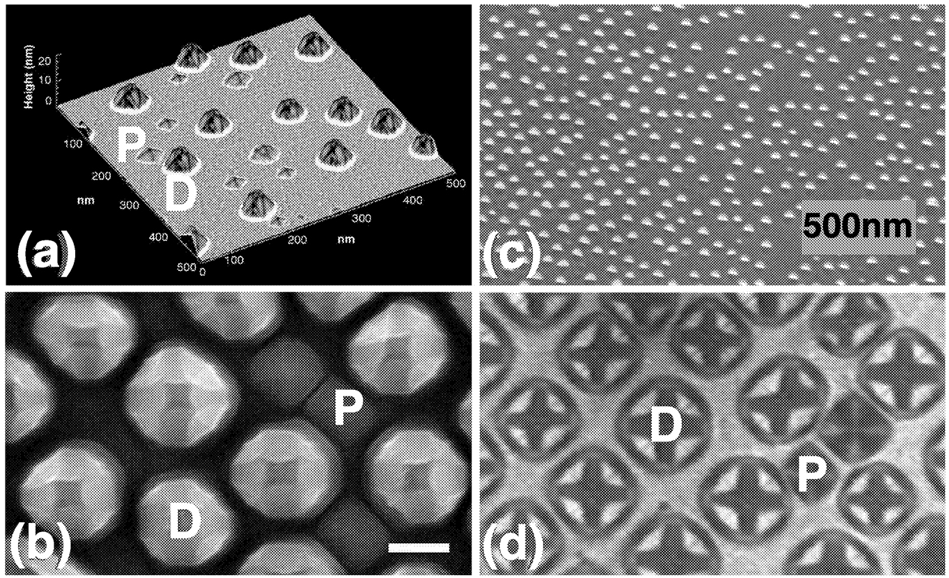
What do quantum dots look like? shows a scanning tunneling microscopy image (Medeiros-Ribeiro et al., 1998) of Ge quantum dots grown on Si(001). Figure 2bshows a scanning electron microscopy image (Ross et al., 1999) of SiGe quantum dots. These images were obtained after the sample had
Page 97
been removed from the growth chamber. The dots come in two varieties: smaller dots that have a pyramid shape (P) and larger dots that have a dome shape (D). This is not a desirable feature. Ideally, all dots should have the same shape and the same size. Figure 2c shows an image of Ge quantum dots on Si(001) taken with an in situ transmission electron microscope (Ross et al., 1998) while the quantum dots were grown. The shape information is lost, but the size of the dots can be measured accurately, and growth can be followed in real time. This allows a detailed study of the time evolution of the quantum dot size distribution.
It has been found (Medeiros-Ribeiro et al., 1998; Ross et al., 1998) that the originally broad size distribution first bifurcates and then narrows significantly when, with continued growth, P dots disappear from the population and most dots take on the D shape. This process can be followed in even more detail with low-energy electron microscopy (Ross et al., 1999), as demonstrated in Figure 2d for SiGe quantum dots. Now both size and shape can be determined in detail, and in real time, during in situ quantum dot growth inside the microscope.
~ enlarge ~
FIGURE 2 Images of Ge (a,c) and GeSi (b,d) quantum dots on Si(001): (a) Scanning Tunneling Microscopy, (b) Scanning Electron Microscopy, (c) In-situTransmission Electron Microscopy, (d) In-situLow Energy Electron Microscopy. Both pure Ge and GeSi alloy quantum dots show two distinct shapes, pyramids (P) at small volume and domes (D) at large volume. SOURCE: Panel a—Reprinted with permission from Medeiros-Ribeiro et al. Copyright 1998 American Association for the Advancement of Science. Panels b & d—Reprinted with permission from Ross et al. Copyright 1999 American Association for the Advancement of Science. Panel c—Reprinted with permission from R. Tromp (Ross et al., 1998). Copyright 1998 by the American Physical Society.
Page 98
The change of the shape of quantum dots with increasing volume is not unique to SiGe. Theoretical studies (Liu et al., 1999) suggest that this is a rather universal phenomenon, although the detailed shapes are different for different systems. In the growth of quantum dots on a substrate, the shape is determined by the balance of surface and strain energies. For quantum dots grown in liquids, other factors may play a role as well. For instance, magnetic dots may change from spherical to ellipsoidal when, above a certain size, crystal anisotropies become significant.
Quantum dot properties can be studied by optical methods ( Figure 1), by microscopic methods ( Figure 2), and by a whole host of analytical techniques that are routinely applied to bulk materials. X-ray diffraction, magnetic measurements, and electrical transport measurements are examples of such techniques. Depending on the properties of interest, one chooses the appropriate analytical method. Some methods allow the study of single quantum dots. The microscopy methods shown in Figure 2are examples, but optical studies of single quantum dots are also feasible (Nirmal et al., 1996). The electronic properties of single dots have been studied using electron energy loss in a special-purpose scanning transmission electron microscope (Batson and Heath, 1993). To date, magnetic measurements and X-ray diffraction measurements have only been performed on ensembles.
APPLICATIONS
The excitement about nanotechnology is based on the conviction that such novel materials as quantum dots have new applications that more conventional materials do not offer. Numerous applications have been proposed for quantum dots, some of which I review here, without any attempt to be complete.
Quantum dot lasers (Eberl, 1997) are among the earliest applications of quantum dots. The semiconductor laser inside a CD player uses a so-called quantum well sandwiched between Bragg reflectors for its laser action. The quantum well presents strongly confined electronic states in a two-dimensional sheet. Inversion can be obtained by injection carriers into the quantum well. The idea behind a quantum dot laser is that the quantum dots naturally provide strongly confined electronic states in zero dimensions. Quantum dot lasers have been successfully manufactured, although they have not displaced quantum well lasers. The problem is at least in part due to control. Molecular beam epitaxy and chemical vapor deposition, the leading methods for fabrication of quantum well lasers, give excellent control over the thickness and composition of the two-dimensional quantum well. Such control is more difficult for quantum dot growth. Relatively broad size distributions, as well as partial strain-driven inter-mixing with the substrate, lead to a broadened distribution of quantum dot electronic and optical properties and loss of laser efficiency. The development of
Page 99
quantum dot lasers continues to be pursued vigorously, and further advances might be seen in the future.
Color converters naturally come to mind when looking at Figure 1b. With the advent of solid-state ultraviolet lasers (GaN in particular), cheap sources of intense ultraviolet radiation are just over the horizon. Such lasers have the potential of becoming a “universal” light source when combined with suitable color converters. Display applications require red, green, and blue pixels. III-V quantum dots fluoresce in the full visible range and are a natural candidate for color conversion applications. Chemical self-assembly methods might enable bulk manufacturing at competitive cost.
Single Electron Transistors (SETs) (Matsumoto, 1996) use the extremely small electrical capacitance of quantum dots to create a novel type of field-effect transistor. Source and drain are coupled to the quantum dot by tunnel junctions. The quantum dot potential can be set by the use of a gate electrode in proximity to the quantum dot. As the gate potential is varied, the source-to-drain conductance oscillates with gate voltage intervals that correspond to the charging voltage of the quantum dot because of the addition of a single electron. The earliest SETs were often realized in two-dimensional electron gas structures in III-V semiconductors, but, more recently, a broad range of materials systems have been used, including Si. And although SETs initially only worked at cryogenic temperature, room temperature versions have now been reported. The temperature of operation is directly related to quantum dot size. With decreasing size the capacitance of a quantum dot becomes smaller, and the charging voltage due to the addition of a single electron increases correspondingly. This charging voltage must be significantly larger than the thermal energy, kT, if the device is to operate succesfully.
Much beautiful physics has been done using SETs, and both storage and logic circuits based on SETs have been proposed, although the practical development of such circuits has been slow. Of course, for commercial applications not a few circuits are required but hundreds of millions, even billions, on a single chip. Excellent uniformity and reproducibility of individual device operating characteristics are musts. Manufacturing control can be good in large devices (i.e., based on two-dimensional electron gas materials), but such devices work at cryogenic temperatures. Fabrication and control of room temperature devices with much smaller dimensions are much more difficult and have suffered from lack of control and device yield.
Quantum computing (DiVincenzo, 1995) is one of the hottest areas in information physics. For certain tasks, quantum computing promises to be far more efficient than digitial computing—at least on paper. At present, however, the theory of quantum computing far outstrips the practice. Experimentally, it is hard to construct the superposition of quantum states that quantum mechanics addresses with such ease. A number of different schemes are being pursued, including nuclear magnetic resonance-based methods (Gershenfeld and Chuang,
Page 100
1998) and superconducting Josephson junction technology (Mooij et al., 1999). An alternative scheme (Loss and DiVincenzo, 1998) is based on the use of small ensembles of quantum dots. The requirements are quite daunting, particularly with respect to uniformity and control.
Nanocrystal semiconductor memory(Tiwari et al., 1996) is another application based on the small capacitance of quantum dots (or “nanocrystals,” as they are often called in this context). In a conventional field effect transistor inversion is obtained by applying a suitable bias voltage to the gate. The incorporation of nanocrystals in the gate insulator would provide a means to apply a field offest by charging the quantum dots. Working devices have been successfully manufactured.
Patterned media (White et al., 1997) are widely discussed as the next step in magnetic storage. It has been proposed that, rather than use continuous magnetic thin films, researchers divide the film in spatially separated magnetic dots, where a single dot stores a single bit. This has certain advantages in terms of the ultimate storage density but is itself limited by the paramagnetic effect at a density of about 100 gigabits per square inch. When the bits become too small, the magnetic moment is subject to thermal fluctuations, and the stored information is subject to thermal decay. Recent attempts at fabricating magnetic nanocrystals have shown much progress, and studies of their magnetic properties are under way. As mentioned earlier, these studies represent ensemble averages over large numbers of particles, which significantly complicates matters. Even if the size distribution is very narrow, variations in orientation, together with crystal and shape anisotropies, may give rise to variations in magnetic behavior from particle to particle. For applications in patterned media, these particles must furthermore be placed in well-defined locations according to a precise architecture, over macroscopic areas. This entire research area is presently in a basic stage, with practical applications some years away.
Hard magnetic thin films (Sun et al., 2000) have been fabricated using magnetic nanocrystals, even though the use of such nanocrystals in patterned magnetic media is not imminent. The magnetic FePt nanocrystals are fabricated using wet chemistry methods discussed above. A substrate can be exposed to a solution containing these nanoparticles. As the solvent evaporates, the nanocrystals condense on the substrate, often in a crystalline network. Sun et al. (2000) recently demonstrated that such magnetic films, after suitable annealing, have magnetic properties that are superior to conventional magnetic films prepared by sputter deposition. These films represent an interesting application of quantum dots and nanocrystalline materials that is not to be overlooked: quantum dots as raw material in bulk quantities, used to assemble new nanostructural materials with superior mechanical, electrical, magnetic, or thermal properties.
Thin-film semiconductors are another example of such an application. Photoconductive properties of CdSe-based thin films have been explored, with potential solar cell applications in mind (Leatherdale et al., 2000). This may
Page 101
easily be broadened (at least conceptually) to other semiconductors. In thin-film transistor liquid crystal displays, amorphous Si is currently used for the switching elements. This material has rather poor mobility compared to crystalline Si, but deposition on a glass substrate is relatively straightforward and inexpensive. Alternatively, nanocrystalline Si deposited by, for instance, screen printing methods could be equally inexpensive, have competitive electrical properties, and may eliminate a few lithographic steps.
Nanostructural inks represent a generalization of the previous two applications. Manufactured in bulk, nanostructural inks can be applied to a wide variety of substrates using a wide variety of application methods, including inkjet printing, screen printing, spray application, spinning, immersion, and so forth. Inks can be mixed, layered, and patterned as applications require. Like the hard magnetic films and solar cells discussed above, new material properties might be realized with the resulting nanostructural solids, at low costs. Nanostructural inks might present the largest opportunity for the practical application of quantum dots and nanocrystals in the next two decades.
Tags are widely used in biology and medicine to allow visualization of specific structures or substances. Gold labeling is a classical example. Chemically prepared quantum dots usually have an organic coating that can be functionalized to interact with specific agents, and they have been used successfully for biolabeling (Bruchez et al., 1998; Chan and Nie, 1998), allowing optical observation by fluorescence. However, the application of quantum dots need not be restricted to biology. Tags are used everywhere for purposes of identification and detection, in areas ranging from research and development to manufacturing and to security. Quantum dot tags, manufactured cheaply and in bulk, offer an interesting alternative to conventional tags.
CONCLUSION
Nanoscale materials present many interesting opportunities and promises as semiconductor device scaling reaches fundamental limits in the near future. Such materials have novel properties that are of interest in a variety of applications— applications not limited to semiconductors. Over the last decade several methods have been developed for the self-assembly of quantum dots and nanocrystals, with varying degrees of control over size and properties. Chemical self-assembly is particularly promising for inexpensive, bulk manufacturing of such materials.
Unfortunately, but not surprisingly, surface and bulk energy terms strongly compete in determining the shape of quantum dots, and the shape may undergo significant changes with size. Therefore, size is not the sole characteristic that matters. Both in situ and ex situ microscopy methods have been developed that enable a detailed analysis of quantum dot size, shape, and evolution. Such studies have clarified some of the basic physics of quantum dot self-assembly, but it is hardly a field that has been explored exhaustively. Some properties
Page 102
(optical, electronic) can sometimes be studied for isolated dots, whereas other properties (magnetic) can only be studied in large ensembles. Many applications require ensembles of quantum dots with very narrow specifications.
Although novel devices have been proposed and some demonstrated in the lab, there are at present no devices, or even device concepts, that threaten to unseat Si. Quantum dot lasers have seen more practical progress but have not yet seen commercial use. Yet, there are numerous applications outside the semiconductor arena that are very promising. Color converters, nanostructural inks, and tags are examples of such applications. The use of nanotechnology on the more macroscopic scale may seem counterintuitive, but, on a short timescale, that might be where the largest opportunities are, with nanoscale devices winking at us from a more distant future.
ACKNOWLEDGMENTS
I gratefully acknowledge numerous colleagues at IBM and elsewhere for stimulating discussions, exchanges, and disagreements, as well as musings and philosophies on nanotechnology.
REFERENCES
, and . 1993. Electron energy loss spectroscopy of single silicon nanocrystals: The conduction band. Physical Review Letters 71(6): 911–914.
, , , , and . 1998. Semiconductor nanocrystals as fluorescent biological labels. Science 281: 2013–2016.
, and . 1998. Quantum dot bioconjugates for ultrasensitive nonisotopic detection. Science 281: .
1995. Quantum computation. Science 270: 255–261.
1997. Quantum-dot lasers. Physics World 10(9): 47–50.
, and . 1998. Quantum computing with molecules. Scientific American. June. Online. Available: http://www.sciam.com/1998/0698issue/0698gershenfeld.html.
, , , , , and . 2000. Photoconductivity in CdSe quantum dot solids. Physical Review B 62(4): 2669–2680.
, , , and . 1999. Equilibrium shapes and energies of coherent strained InP islands. Physical Review B 60(24): 17008–17015.
, and . 1998. Quantum computation with quantum dots. Physical Review A 57(1): 120–126.
. 1998. Special issue on Semiconductor Quantum Dots. MRS Bulletin 23(2). Also available http://bloch.leeds.ac.uk/~ircph/maze/quantum-dot.html.
1996. Room temperature operated single electron transistor made by STM/AFM nano-oxidation process. Physica B 227(1–4): 92–94.
, , , , and . 1998. Shape transition of germanium nanocrystals on a silicon (001) surface from pyramids to domes. Science 279: 353–355.
, , , , , and . 1999. Josephson persistent-current qubit. Science 285: 1036–1039.
Page 103
, , and . 2000. Synthesis and characterization of monodisperse nanocrystals and close-packed nanocrystal assemblies. Annual Review of Materials Science 30: 545–610.
, , , , , , and . 1996. Fluorescence intermittency in single cadmium selenide nanocrystals. Nature.
, , , , , and . 1996. Structural and optical characterization of InAs/InGaAs self-assembled quantum dots grown on (311)B GaAs. Journal of Applied Physics 80(6): 3466–3470.
1999. Pushing the limits. Science 285(5436): 2079–2081.
, , and . 1998. Coarsening of self-assembled Ge quantum dots on Si(001). Physical Review Letters 80(5): 984–987.
, , and . 1999. Transition states between pyramids and domes during Ge/Si island growth. Science 286: 1931–1934.
, , , , and . 2000. Monodisperse FePt nanoparticles and ferromagnetic FePt nanocrystal superlattices. Science 287: 1989–1992.
, , , , , and . 1996. A silicon nanocrystals based memory. Applied Physics Letters 68(10): 1377–1379.
, , and . 1997. Patterned media: A viable route to 50 Gbit/in/sup 2/and up for magnetic recording? IEEE Transactions on Magnetics 33(1)(Part 2): 990–995.


