
4
Enabling Manufacturing Technologies
Much of what is called manufacturing science applies to a very wide range of products and size scales. Manufacturability and quality control, which are closely related, vary widely with the type and specifics of a product, whether for the military or for mass markets. Production of microscale surface finishes on a material (for example, a polished metal surface on an aircraft engine turbine blade) is certainly different from making parts for MEMS devices on a similar size scale (for example, a microaccelerometer with submicrometer feature sizes). Similarly, the production of nanocrystalline materials is generally very different from the manufacture of possible molecular electronic devices. In this chapter, the committee considers the general aspects, along with some particular aspects, of manufacturing products whose performance depends on structure, material, or chemistry on the micro- and nanoscales.
The materials, components, subsystems, systems, and platforms used by the military are mainly purchased from industry. Rarely is military hardware manufactured by the Department of Defense. Hence, industry-based manufacture of what the military uses is of central importance. This will be no less true for hardware made by micro- and nanotechnologies than it is for the alloys, antennas, radars, missiles, and airplanes that are now being employed by the military. The role of various communities in acquiring, maintaining, and employing military hardware is summarized in Figure 4-1.
FABRICATION (PATTERNING) APPROACHES
Integrated circuit manufacturing is a top-down process where the starting point is a flat wafer onto which patterns are defined and created by both additive
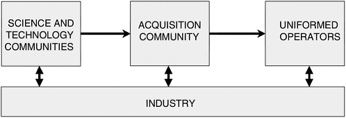
FIGURE 4-1 Communities needed for the production, maintenance, and use of military hardware.
(thin-film deposition and growth) and subtractive (etch) processes. This has evolved into an enormously sophisticated enterprise, which is proven for the low-cost, high-yield manufacture of extremely complex (~100 million transistors) and reliable circuits. However, limitations are on the horizon. One is the difficulty of extending today’s optically based lithographic techniques to the nanoscale, which is much smaller than ultraviolet optical wavelengths. Another is the limited number of materials used in ICs. The nanotechnology community is investigating many disparate technologies based on many different materials, but it is far from evident that the different processing requirements of these technologies can be reconciled.
Self-assembly is a radically different approach to fabrication at the nanoscale. It takes advantage of molecular and intermolecular forces to define atomic, nanoscale, and macroscale structures. Self-assembly depends on appropriate direction and control being exerted at all stages of the process by preprogramming of the subunits or building blocks such that the required recognition elements for self-assembly are contained in the subunits. Crystal growth is an example of self-assembly with exquisite long-range order. Living species are proof that complex three-dimensional structures with interacting functionality are possible. Integration of the top-down (lithography and pattern transfer) and the bottom-up (self-assembly) approaches offers an attractive approach to bridging the current gaps between these paradigms.
The incompatible materials issue may be addressed by individualized optimization of different devices and subsystems, followed by an assembly process akin to the automotive assembly line but at a vastly smaller scale. Here again, top-down (pick-and-place) and bottom-up, self-assembly inspired (DNA-assisted) approaches are among the many being investigated.
Lithography and Pattern Transfer
The microelectronics, computer, and information revolutions can trace their success to several technological roots. The integration of transistors into functional blocks—which are further integrated to form microprocessors, memories, and other ICs—is one of the main reasons for the ever-increasing functionality. Decreasing linewidths, currently 130 nanometers, enable placing more transistors on a chip. Increasing wafer sizes—now up to a 300-millimeter diameter, with projections to 400 millimeters—allow more chips to be produced simultaneously. Mass production of integrated circuits by batch fabrication with high yields has led to declining cost per function and the remarkable reliability of microelectronic devices. Not having to assemble individual parts before packaging chips has also been a major factor in the high yields and low costs of microelectronics. A great triumph of microelectronics has been the high-yield manufacturing of reliable 100-million-part assemblies. With nanotechnology, reliability of even more complex assemblages is possible.
There are fundamentally only two kinds of things that have to be done to produce integrated circuits—a pattern must be made and it must be transferred into the work piece by either deposition or removal of materials.1 The pattern definition is done by lithography. Pattern transfer involves any of a number of processes for adding materials to a wafer, such as ion implantation, or removing materials, such as plasma etching. Ancillary techniques are also employed to ensure that the pattern production and transfer techniques work properly. Planarization of a partially processed wafer by chemical-mechanical polishing is an example.
Currently, lithographic exposures are done between 24 and 30 times or so during production of a complex IC. Each exposure requires multiple processing steps, including spinning on, prebaking, exposing, postbaking, developing the resist, pattern transfer, and removing the residual resist. Indeed, there may be about 200 processing steps for a modern integrated circuit. Today the mask sets for the most sophisticated circuit can cost about $1 million. The systems that align a given mask level to structures on a wafer and make the exposures cost about $10 million. Aligners are projected to cost close to $30 million in 5 years.
Lithography enables production in many technologies besides integrated circuits. Figure 4-2 shows several of the classes of structures and devices that require lithography to produce a pattern on a substrate. The highest resolution lithography is generally required only for cutting-edge integrated circuits. However, techniques developed in the IC industry clearly have applications to many other fields. In the top row of Figure 4-2 is an etched integrated circuit with its copper interconnects, a flexible printed circuit board, and solder bumps. The center row shows a deep-etched silicon structure, a photonic material, and a microfluidic device. In the bottom row are a gene chip, densely packed nano-crystals, and guided cell growth.
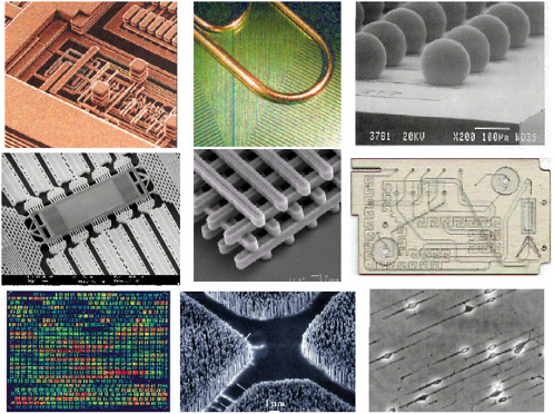
FIGURE 4-2 Lithography examples. SOURCE: Nagel, D.J. 2002. Technologies for micrometer and nanometer pattern and material transfer. Direct-Write Technologies for Rapid Prototyping Applications, A. Pique and D.B. Chrisey, eds. New York, N.Y.: Academic Press. © 2002, Elsevier Science (USA), reproduced with permission of the publisher.
Currently, most aligners use 248-nanometer radiation from KrF lasers to expose photoresist. The switch to ArF lasers, which have a wavelength of 193 nanometers, has already begun for the production of chips with 100-nanometer linewidths. In a few years, the ITRS indicates that it will be necessary either to continue this migration to a 157-nanometer wavelength advanced optical lithography tool or to switch to a next-generation lithography approach. Both alternatives are being intensively investigated and are likely to coexist for some time.
The leading contender in the United States for the next lithography technology is extreme ultraviolet (EUV) radiation with a wavelength of 13 nanometers.2 EUV lithography requires the use of plasma sources produced by high-power laser irradiation of atomic xenon, all reflective optics (including the mask), and— as usual for a different wavelength—new photoresists. Numerous technical barriers must be overcome for EUV lithography to be ready for the production of commodity ICs.
In Japan, there is still strong interest in x-ray lithography using 1-nanometer wavelength radiation.3 In this case, the “light” source would be either plasmas or high-energy electrons orbiting in an evacuated toroid, so-called synchrotron ra-
diation. A fundamental challenge with x-ray lithography is the mask, which must have features the same size as the pattern to be impressed into the photoresist. That is, x-ray lithography is a one-to-one technology and not a projection reduction technique, because optical elements that focus 1-nanometer radiation are not available.
Techniques to further extend optics using alternative exposure schemes and various nonlinear processes in the lithography process are also under investigation. It is far from clear which lithography technique will prove to be the industrial workhorse for ICs with linewidths below 100 nanometers. It is possible that electron projection or direct-write technologies will play some role in future chip production. For large-volume commercial applications, economics will be a major driver. Evolution of an incumbent technology, e.g., optical lithography, almost always wins until fundamental limits are reached. For optics the fundamental limit is related to, but is not the same as, the optical wavelength. In a single exposure the limit is on the highest spatial frequency, or how close together two features can be located, not on how small each feature can be. This limit is approximately one-fourth of the wavelength, or 50 nanometers for today’s ArF-laser-based lithographic tools. Immersion techniques allow a reduction by a factor of about 1.5, the refractive index of the immersion fluid. Multiple exposures taking advantage of inherent nonlinearities in the photoresist and subsequent processing stages allow further extensions by factors of one-half, one-third, etc. The manufacturing limits for these optics extensions are associated with process latitude and yield rather than with fundamental physical limitations.
It is clear that lithography for the volume production of microelectronics is already a nanotechnology and will become increasingly so in the next decade. Moreover, it will be a long time before any of the methods of modern nanotechnology, such as the growth and use of carbon nanotubes, rival lithography in commercial volume.
Beyond the methods that are in use or in contention for mass production of integrated circuits, a number of lithographic methods have been developed in the past decade. Not all of them offer the nanometer resolution that will be needed for IC production in coming years. However, they have been or might prove to be of use for making some MEMS and other structures and devices. These methods are briefly reviewed before discussing pattern transfer methods.
A three-stage process, developed in Germany, involves sequential use of lithography, electrodeposition, and molding (Lithographie, Galvanoformung, und Abformung) (LIGA). In contrast to the lithography technologies surveyed so far, which use resists with thickness from nanometers to micrometers, LIGA employs resists with thickness from micrometers to more than millimeters. The steps in the LIGA process are shown schematically in Figure 4-3.4
The next lithography method is both the most recently discovered and the most unconventional compared with commercial techniques. It is called lithographically induced self-construction (LISC),5 and it has a variant termed litho-
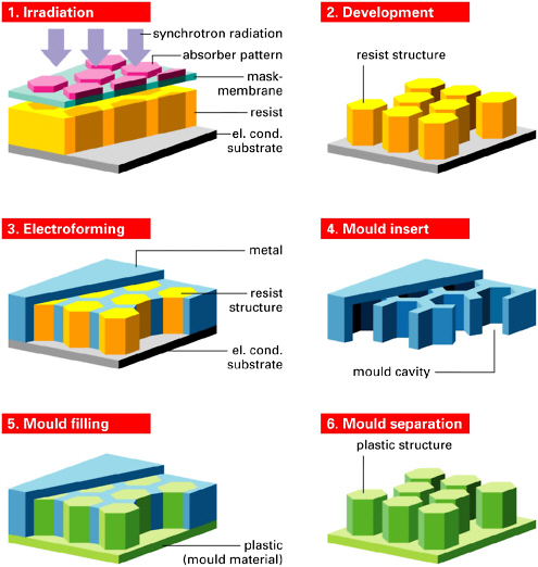
FIGURE 4-3 The sequential steps in LIGA. In 1 and 3, el. cond. means electrically conductive. SOURCE: Institut für Mikrotechnik Mainz GmbH. 2001. LIGA Technology. Available online at <http://www.imm-mainz.de/> [August 12, 2002].
graphically induced self-assembly (LISA).6 In both cases, a patterned mask coated with a surfactant is placed in close proximity to a substrate covered with a thin thermoplastic polymer (Figure 4-4). The polymer may be chemically identical to a photoresist—for example, polymethyl methacrylate (PMMA)—but it does not function as a normal photoresist. There is no radiative transfer between the mask and polymer, and the chemistry of the polymer is not modified during pattern transfer. Rather, when the PMMA is heated to 170°C (which is above the softening point), electrostatic forces cause it to move laterally into shapes mediated by the nearby mask. The LISC and LISA techniques are both hybrid contact and
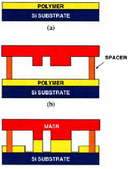
FIGURE 4-4 Schematic of the structures used in LISC. SOURCE: Reprinted with permission from Chou, S.Y., L. Zhuang, and L. Guo. 1999. Lithographically induced self-construction of polymer microstructures for resistless patterning. Applied Physics Letters 75(7): 1004–1006. © 1999, American Institute of Physics.
proximity methods. In LISC, the resulting pattern is determined only by the pattern used. In LISA, the pattern that is produced has an overall shape set by the mask but fine details within that shape that arise spontaneously.
Embossing is one of the old technologies that has been extended to the micrometer scale in recent years. Hot embossing can be employed to produce micrometer and even nanoscale features and structures. Patterns with structures about 10 μm wide and deep can be embossed into PMMA.7 Recently, a modified wafer bonding system was used to emboss structures as fine as 400 nanometers across an entire 10-cm-diameter wafer.8
A variant of embossing, called nanoimprint lithography (NIL), involves impressing a mold onto the surface of a photoresist-covered substrate.9 In this case, the pattern is transferred to the resist, commonly PMMA, by mechanical rather than chemical action. Subsequent processing of the resist to open the thinned regions to the substrate permits conventional uses of the resist for deposition onto or etching into the substrate. The molds for NIL can be prepared by a wide variety of the normal and developmental lithographic processes. For example, e-beam lithography has been used to make a mold with 10-nm-diameter pillars on a 40-nm pitch that were then imprinted into PMMA.10
A technique called step and flash imprint lithography essentially embosses a layer of liquid on a surface that is then turned into a solid using a photochemical process.11 This technique avoids the elevated temperatures and pressures ordinarily required for embossing. The wafer is first coated with a transfer layer of solid organic material. Then a glass template with the desired pattern is placed near the coated wafer. The template can be micromachined by a variety of meth-
ods. A low-viscosity liquid (a photopolymerizable, organosilicon etch-barrier material) is dispensed between the template and transfer layers on the wafer, and the layers are then brought into contact. After UV exposure to solidify the etch barrier and make it adhere to the transfer layer, the template is removed. A plasma etch transfers the pattern from the now solid etch barrier into the transfer layer, and then the etch barrier is removed. This leaves the pattern in the transfer layer on the wafer surface ready for further processing steps. Step and flash imprint lithography has produced 60-nanometer features.
Rubber stamps have been used for centuries. In recent years, Whitesides and his group have extended stamping to replicate patterns with features finer than micrometers by the use of polydimethylsiloxane (PDMS) and other elastomers. They term the technique “soft lithography” because of the compliant character of the stamp.12 One of the ordinary lithography methods is used to pattern a thin film on silicon or some other substrate to make a mold. After the surface of the mold has been etched and silanized, the liquid PDMS precursor is cast over the pattern and polymerized by cross-linking. Then, the elastomer is peeled off the mold and placed on a substrate for handling. Wetting of the PDMS stamp with various liquids and suspensions is done before the stamping. In general, the depth of the pattern is in the range of 0.2 to 20 μm, with the maximum limited by the stability of the PDMS structure. The width and spacing of the contact regions are between 0.5 and 200 μm, with the separation limited by the tendency of the region between contacts to bulge toward the substrate being stamped. Soft lithography can be employed in a rolling manner if the PDMS stamp is attached to a cylinder.
The methods for pattern production and transfer that are used in the manufacture of microelectronics IC production involve a very limited number of materials and associated processes. The materials used for chips now number only about 10. Copper interconnects, high-dielectric-constant (k) materials for gate insulators and low-k materials for separating interconnect lines are the most recent additions to the list of IC materials. The processes used to make these materials during chip production also number about 10.
IC technologies are certainly fundamental to the production of microscale mechanics, optics, and magnetics. However, the number of materials and processes in demonstrated and emerging MEMS and similar technologies far exceed those used for IC production, as indicated schematically in Figure 4-5. One example is the use of piezoelectric materials in MEMS for linking electronic and mechanical behavior. The substrates employed for MEMS devices include semiconductors other than silicon, notably silicon carbide, as well as ceramics, metals, and polymers.
There are numerous processes used in the manufacture of MEMS devices that play no role in IC production. The central step in the production of micromechanics on a substrate by surface micromachining is the dissolution of a sacrificial layer of material to release the mechanism. Deep etching of a substrate, called “bulk micromachining,” is another important MEMS pattern transfer tech-
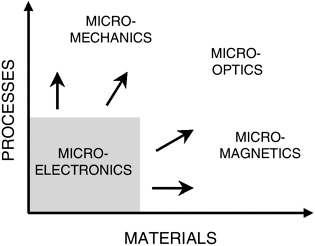
FIGURE 4-5 Integrated circuit production. The number of materials and associated processes for the production of micromechanics, -optics and -magnetics greatly exceeds the number of materials and processes used to manufacture microelectronics.
nology that has no role in IC manufacture. Such etching is done by one of two processes. The use of solvents, which attack different planes in silicon at widely varying rates, is called orientation-dependent etching. It now plays a role in the production of some MEMS products. The alternative is deep reactive-ion etching (DRIE). In this case, the plasma ambient over a silicon substrate is alternated every few seconds between etching and passivation (coating) conditions. This process, invented by the Bosch Corporation, can result in deep, narrow trenches in the substrate, the walls of which are scalloped on a very fine scale. Figure 4-6 shows examples, and it also indicates that the rate at which the Bosch process etches into the silicon is geometry dependent.13
The role of pattern transfer for the production of nanoscale structures and devices will probably be similar to that for the production of microscale structures and devices involving mechanics, optics, and magnetics. That is, the transfer processes used in microelectronics manufacture will remain important in many cases. The self-assembly of complex structured materials, as discussed in the next section, is playing an increasingly important role in nanoscale fabrication. New approaches using lithography to direct self-assembly are already emerging in fields as disparate as semiconductor crystal growth (discussed below) and carbon nanotube formation and are likely to play a significant role in the development of nanotechnology. The wider variety of materials that will play a role in nanotechnology will probably involve additional techniques for pattern transfer. This will almost certainly be the case for nanoscale structures that use organic and biomaterials.
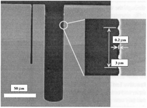
FIGURE 4-6 Cross-sectional photograph of a silicon wafer processed by deep reactive ion etching. SOURCE: S.D. Senturia. 2000. Microsystem Design, p. 70. Boston, Mass.: Kluwer Academic Publishers.
Self-Assembly
Self-assembly in nature is older than life itself. Crystalline geological structures spontaneously form highly organized patterns from molten lava. All living organisms, from the simplest single-cell species to humans, depend on some form of molecular self-assembly. Nature performs the most astonishing feats of self-assembly with an artistry and facility that we can only admire and all too often take for granted. Protein folding, nucleic acid assembly and tertiary structures, phospholipid membranes, ribosomes, microtubules, and the nucleocapsides of viruses are but some, representative examples of biological self-assembly in nature that are of critical importance to living organisms.14
Aside from their ability to carry out the functions of life, one of the more remarkable features of self-assembled materials is that their structure may be very complex yet demonstrate long-range order. The power and beauty of spontaneous self-assembly derives from its ability to rapidly, and with seeming ease, generate large, complex, sophisticated “supermolecules,” or ensembles of molecules, from easily available building blocks with high efficiency, generally under mild conditions (at or near room temperature, at atmospheric pressure, in water or other common media). A biological self-assembly,15,16,17 as exemplified by such structures as crystals,18,19 surfactants,20 micelles (nanoscale molecular aggregates),21 colloidal suspensions in confined films or aggregated into fractal structures,22 self-assembled monolayers (SAMs),23 and liquid crystals,24 involves ensembles of molecules with unique properties and function. Because it is possible to manufacture nanostructures with useful properties through self-assembly, interest has recently increased substantially in the study of interactions of molecules that form larger nanostructures of ordered material aggregates.
Nature’s repertoire of information to guide self-assembly includes hydrogen bonding, π-π stacking, electrostatic and van der Waals interactions, hydrophobic-hydrophilic interaction, dipolar effects, molecular conformations, and phase boundaries, as well as the shape and size of both the final product and the constituent subunits. These effects are commonly referred to as weak interactions in contrast to the strong chemical bonds characteristic of simple molecules,25 which were the basis of the revolution in chemical products of the last 100 years.
An important feature of all self-assembly processes is the existence of a kinetically labile, reversible equilibrium between starting materials, intermediates, and products,26 with the final outcome under thermodynamic control (i.e., the end ensemble is the thermodynamically most stable one). As the equilibrium is reversible, the process is self-correcting; an incorrectly formed bond can disassociate and reassociate correctly. As a consequence, self-assembly processes generally engage in self-repair and are self-healing.
Self-assembly has the potential for bottom-up fabrication techniques to produce nano- to mesoscale materials and systems, that is, structures and ensembles having spatial dimensions in the range of 1 nm to 1 μm—the size of a large molecule to the size of a living cell. Nano- to microscale systems bridge the molecular and the macroscopic and display unique collective and often nonlinear behavior and properties, different from the bulk characteristics of common substances. Control of the bottom-up products is difficult at present (except for biologically produced and a few select materials) because of the currently limited understanding about how to use these forces. The current state of knowledge about self-assembly and the potential for new products may be comparable to the state of knowledge about the chemical bond at the turn of the previous century. Expanding interest in the fabrication of new materials with these self-assembly methods may give rise to an entirely new discipline.
Examples illustrating the potential of self-assembly as a process for materials production include materials such as the shell of an abalone. This composite material is formed by the careful assembly of elongated calcium carbonate crystals in layers, with the long axes of the crystals pointing in perpendicular directions in alternating layers. A protein deposit forms a strong glue to hold these crystals in place, forming the strong final product.
A wide variety of useful composite whisker structures are formed by a number of mechanisms such as condensation on specific crystal faces, selected chemical reactivity, and eutectic behavior of alloy mixtures. An example of a fascinating nanostructure formed through the forces involving chemical bonds is that of a carbon nanotube. Selected nanotubes with high conductivities have excited researchers because they might one day be used as conductors and circuits in nanoelectronics (see Box 3-1).
Block copolymers form amazingly regular patterns of plastic material with repetition distances on the order of nanometers to micrometers. These plastics interact with light and are used in devices such as optical band gap structures for
optical communications. Block copolymers can be etched to form porous arrays of regularly spaced voids. Porous materials may be formed that have selected void dimensions for specialized catalytic activity. Likewise, dendrimers and dendrimer assemblies,27 as a result of their globular shape, their layered architecture, their well-controlled size, and their unique optical and electronic properties, may find uses in micro- and nanoelectronics and other applications.
When fully developed, bottom-up fabrication using self-assembly and related methodologies will be able to produce ordered, precisely controlled nano-materials and nanodevices not achievable by current methods such as lithography and other top-down techniques.28 Recent examples of interest include novel protein-based materials such as artificially modified spider dragline silk, mussel byssus thread, elastin, and other higher-ordered aggregates derived by protein engineering.29 Other directions of self-assembly research include genetic methods of polymer synthesis;30 kinesis-powered microdevices (molecular motors);31 nano-optics in the biological world;32 molecule-based magnets;33,34 biomedical applications;35 and molecular-based materials in electronic devices, light-emitting diodes, quantum dot lasers, and photovoltaic devices.36
As a field of endeavor with widespread applicability, self-assembly is just beginning a new era for the production of new materials.
Integration of Traditional Lithographic and Self-Assembly Patterning Approaches
One of the grand challenges of nanoscience is precise positioning, atom by atom. Historically there have been two approaches to this challenge: top-down lithography and bottom-up self-assembly. Lithography has made enormous strides during the development of the integrated circuit. As discussed above, present lithographic limits are in the 100-nanometer range. New techniques are being developed that will reduce this scale by approximately an order of magnitude, still far from a typical molecular interatomic distance of approximately 0.5 nanometers.
From the other direction, using self-assembly techniques, chemists routinely make molecules, literally by the boxcar full, with precise distances between atoms. Crystals are beautiful examples of precise self-assembly with long-range order. On a 300-mm-diameter silicon wafer, if you know the position and orientation of a single unit cell, you know—to within variations due to temperature, stress, impurities, and thermal motion—the precise positions of the atoms on the other side of the wafer, or at the other end of the boule. Recent explorations of molecular self-assembly have sought to provide transverse dimensions on the mesoscopic nanometer scale. As a general—although not inviolate—rule, these attempts have led to very good local ordering (e.g., nearest neighbors) and comparatively poorer long-range order (on macroscopic dimensions). This is inherent
in techniques that provide multiple nucleation sites, for example on a flat, non-crystalline surface. Multiple crystal domains nucleate as dictated by the thermodynamics of the process, and grain boundaries result as the individual crystallites grow and merge.
One active direction of research is to meld these two techniques and use each to its best advantage. Top-down lithography can provide a very high degree of long-range order on from the centimeter scale down, with features that now extend down to about 100 nanometers. Molecular self-assembly works well below the 10-nanometer scale. These regimes are close enough that they will merge and offer the possibility of complete control from the macroscopic to the atomistic. Nanotechnology will likely demand control across all of these spatial scales.
In the information technology domain, a further motivation for addressing all of these scales is that the new nanoscience functional elements—e.g., the equivalent of the transistor and its interconnections—are most likely to be used in combination with our existing silicon-based electronics infrastructure. Thus, we will already have the top-down processing in place.
In the vertical dimension, there are many examples of using self-assembly as a very precise ruler. The exceptional precision of today’s epitaxial growth techniques was discussed in connection with quantum wells in the first section of Chapter 3, “Information Technology.” As a result of this precision, it is literally possible to count atoms as an epitaxial layer is being grown and stop when that layer is any integral number of atomic layers thick. In some cases, one can even transmute the layers after they are grown, as is done in the case of defining l/4 distributed Bragg reflection mirror stacks for vertical cavity lasers by selective oxidation of high aluminum content AlxGa1−xAs layers to aluminum oxide.37 Recent reports have discussed using similar techniques in the transverse dimension by building up a set of molecular multilayers at the edges of masks defined by top-down lithography.38 These approaches are still in their infancy, and much has to be done to mature them into useful applications. They represent one of many conceivable ways of combining the top-down and bottom-up approaches to define nanoscale features.
Semiconductor Epitaxial Growth—An Example of the Integration of Bottom-Up and Top-Down
Semiconductor growth is a rich arena for innovations in patterning. The recent interest in three-dimensional confinement (quantum dots) and in photonic crystals (see section on optical devices in Chapter 3) has led to a spurt of activity. Traditional semiconductor epitaxial growth is carried out on large-area substrates, up to 300 mm in the case of silicon. While there is a rich tradition of growth on patterned surfaces, the scale of these surfaces has traditionally been several micrometers or larger, used primarily to define isolated growth areas.
Two notable early exceptions were (1) the use of slightly misaligned silicon substrates with a well-defined series of atomic steps to reduce antiphase disorder (both Ga-rich and As-rich <100> faces of GaAs nucleate on a Si <100> face) in the growth of GaAs on silicon,39 and (2) the use of etched V-groove structures as substrates for the growth of quantum wires just at the apex of the V-groove.40 Neither of these early attempts at nanopatterned growth proved successful for growing device-quality material because of issues associated with remaining defects. A successful microscale patterned growth approach has been the use of the dependence of growth rate on area and on crystal face in the case of deeply etched structures to achieve multiple wavelength devices in the same growth.41 This is particularly important for network wavelength division multiplexing (WDM) applications, where a range of wavelengths is required. Having all of the sources (and possibly matched detectors) on the same substrate is an important packaging advantage.
With the increasing ability to fabricate nanostructured substrates, there is increasing interest in epitaxial growth at these dimensions, an area that is largely unexplored. One specific direction is the use of nanostructured growth for heterogeneous material systems with significant lattice and thermal mismatches between the film and the substrate.42 Much of this interest has been spurred by the device applications of wide bandgap GaN and related materials for which there is as yet no suitable bulk substrate. Applications are both commercial (visible LEDs and lasers, high-frequency and high-power electronics) and military (solar-blind detectors, UV sources for chemical and biological agent detection, high-frequency and high-power electronics). Microscale structured substrates have been successfully developed based on epitaxial lateral overgrowth (ELO), where the film is allowed to nucleate in only small areas and grows laterally over the masked areas with many fewer defects. Nanostructured materials, including self-assembled porous substrates, block copolymer films, and lithographically defined patterns, are being investigated. There appear to be several advantages to the nanoscale in that nanoscale seeds reducing the epitaxial film strain can accommodate some of the lattice mismatch. Also, the local free surface associated with the nanoscale appears to modify the character of the remaining defects, in some cases resulting in a confinement of these defects to the near interface region. Much more work is needed to determine the utility of these results for actual device materials, but the initial results are promising.
The direct fabrication of quantum-confined semiconductors is another important direction. As noted in Chapter 3, attempts to define quantum dots by subtractive processes (etching) have been stymied by significant defect densities, which lead to rapid nonradiative recombination. Growth processes wherein a nanoscale mask is first defined and the material is then grown have shown some promise, but still exhibit poorer photoluminescence than fully self-assembled materials and have not yet produced device-quality material. Nanoscale patterned growth remains a promising active area of research with potential for important
advances. An alternative direction that shows nascent promise is the adaptation of some of the techniques used to grow carbon nanotubes to more traditional semiconductor materials—both Si and III-V materials.43,44 These techniques have now been extended to junctions, heterostructures, and superlattices demonstrating a wide array of functionality, including light emission and electronic non-linearity.45
Integration of Nanodevices with Mainstream Silicon Technology
Modern electronics is based on silicon technology. As noted elsewhere in this report, progress in silicon technology and manufacturing has been steady for perhaps 50 years and is projected out at least 15 years into the future and certainly well into the nanoscale regime. This progress and the utility of electronic semiconductor products caused semiconductor manufacturing to become one of the largest industries in the world and certainly one of the most sophisticated and creative.
The latest release of the ITRS46 forecasts significant difficulties over the 2002-2017 time frame in various perhaps fundamental aspects of the scaling that has held for so long. As detailed in Chapter 3, this has led to a host of efforts to discover the successor to silicon. The ultimate utility of any of these pretenders to the silicon crown is uncertain, and predictions of test-tube microprocessors seem premature. Some numbers make clear the issues: today’s most advanced memory chips contain on the order of 109 transistors, interconnected in a complex pattern involving a hierarchy with both local and global character. Not only the internal functioning, but also the input/output protocol, is precisely defined and matched to the requirements of the microprocessor interface buffer. Together these elements perform an elaborate symphony to provide function. And despite the very large cost of the equipment and manufacturing infrastructure, circuits are produced so quickly and reliably that the cost of computing power, measured in computations per second to the end user, decreased by over nine orders of magnitude as the technology progressed from vacuum tubes to discrete transistors and to today’s advanced microprocessors over the past 50 years.47
In contrast, each of the contenders for silicon’s crown is today largely at the stage of working out what its “transistor” is going to be. Even if this “transistor” turns out to have exceptional performance (which so far remains possible but not proven), there is still a very long way to go to integrate the “transistor” with everything else and produce a computer.
This is not to suggest that research in alternatives to silicon electronics is not warranted. But, it may be that these new technologies will first find use as complements to silicon, not as immediate replacements. We already know how to do so much with silicon it seems unlikely that a new technology will spring up overnight sufficiently developed and robust to supplant not only the transistor but all the rest of the system.
ASSEMBLY
Webster defines the term “assembly” as the “fitting together of manufactured parts into a complete machine”—for example, interfacing disparate components into a functional hybrid unit (think of what an automotive assembly line does). At the beginning of the 21st century, assembly is moving to smaller and smaller dimensions and to very-high-technology processes and materials. This section will discuss two new types of micro- and nanoassembly to illustrate the potential richness of these new, very small assembly methods: directed assembly (e.g., programmed pick-and-place) and fluidic self-assembly relying on either shape keying or DNA-labeling. In many ways the origins of these types are akin to the top-down and bottom-up patterning technologies discussed above.
Directed Assembly
Directed assembly is distinguished from self-assembly, where quasi-equilibrium environments are used to arrange things. (An example of self-assembly is the microfluidics, discussed in the next section.) Directed assembly is programmable assembly, where parts are moved mechanically and placed precisely where they are intended to go.
The impressive gains by the IC industry have been accomplished by parallel processing and monolithic integration. However, monolithic integration has limits, especially as the materials repertoire is increased beyond traditional electronic materials. The lack of a monolithic integration process extending across a wide range of functional materials demands that discrete parts be assembled into a whole. Unfortunately, directed assembly technology has lagged seriously behind monolithic integration in miniaturization. Consider that while an individual transistor is significantly smaller than a micron on a side, the smallest parts that are routinely assembled by today’s automated assembly tools are approximately 1 mm on a side. Not coincidentally, this is essentially the smallest part a human can reasonably manipulate in manual assembly operations.
Robotics and automation experts are starting to build assembly systems to handle parts smaller than 1 mm. However, these systems and their unit operations get more expensive as the parts and required precision of assembly decrease in size. This is true principally because the parts for the automation tools are produced by serial processing (conventional machine shops) and the automation assembly process itself is serial.
Progress in directed assembly needs to take advantage of the high- precision, parallel processing that the IC industry has developed. This strategy will provide a clear path to scaling down components and microsystems, which may be more cost effective than either manual or conventional automation assembly. An example of this type of process is the parallel assembly process being developed by Zyvex, Inc. This company is using silicon MEMS as an integral part of the
assembly system: as a method of arranging parts for assembly, as the fastening mechanism, and as a method for fine positioning adjustments.
Several factors argue for using MEMS to manipulate the parts being assembled. The starting point is that submicrometer dimensional control is readily available through MEMS but is very difficult and expensive with conventional machining. The excellent mechanical properties of silicon are an advantage. Another factor is the well-developed infrastructure that already exists for silicon materials and processing. If there were any questions about the fundamental reliability of MEMS devices, they should have been put to rest with the success of Texas Instrument’s (TI’s) digital light projector chips (see the last section of this chapter for the history of this product), which are by any reasonable measure the most reliable mechanical devices ever created. Finally, there is a clear roadmap for downscaling MEMS that has already been formulated by the IC industry. Direct assembly is aimed at overcoming one of the principal limitations of MEMS processing, its generation of essentially two-dimensional parts. Assembling MEMS parts will enable multiple degrees of freedom of motion.
The key points of this assembly strategy include a movable tether approach that allows parts to be arranged on silicon wafers and constrained in a known position until they are captured. To achieve high throughput, the parts and finished goods are arranged in a periodic array to allow parallel assembly. The parts consist of modular MEMS carriers that have either integrated MEMS devices or preattached component parts. The carriers include silicon snap connectors that make mechanical and, if needed, electrical connections with the assembly substrate. An array of MEMS grippers is attached to the macroscale robotics used to capture parts from the parts array and carry and attach them to the assembly arrays in a highly parallel manner. Figure 4-7 shows an assembled MEMS gripper device, called a rotapod, used to capture and position parts. The rotapod is a MEMS device assembled from two separate MEMS parts using snap connectors. It has a gripper mechanism and is capable of rotating along two axes. This part will be able to capture parts and rotate them into position for assembly, thus breaking out of the dominant two-dimensional MEMS assembly paradigm.
The grippers and snap connectors are designed with self-centering mechanisms that allow significant tolerance in the capture and attachment process. This self-centering capability effectively discretizes the assembly process, allowing high-precision assembly with relatively inexpensive robotics. The silicon snap connectors place components more accurately than the robotics.
The main advantage of such a MEMS-based manufacturing technique over current practices is parallel processing, analogous to the advantage that IC processing enjoys over discrete electronics. Parallel processing should drive down the cost of microsystem assembly.
This assembly manufacturing technology may find its first major application and a large market share in manufacturing fiber-optic communication components. This will allow demonstration of the technology at larger size scales and
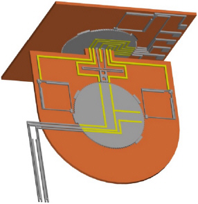
FIGURE 4-7 Rotapod MEMS device. SOURCE: Randall, J. 2001. MEMS/Nano Technology for Assembly of Systems. Briefing by John Randall, Vice President for Research and Chief Technology Officer, Zyvex, to the Committee on Implications of Emerging Micro and Nano Technology, DoubleTree Hotel, Albuquerque, N. Mex., November 8.
will pave the way for assembly of parts smaller than can be handled manually or with conventional automation equipment. Further, once a low-cost assembly manufacturing process is available, many systems being attempted with monolithic integration approaches will find much more success with separate optimized processes for different components that can then be assembled into complex functional units.
DNA-Assisted Assembly
Future photolithographic processes are expected to provide nanoscale metal oxide semiconductor transistors and other semiconductor-type devices. But truly monolithic, heterogeneous integration of photonic, microelectronic, MEMS, and microfluidic components into one chip is both difficult and expensive. The difficulty arises from the incompatibilities of the functional materials and of the various fabrication processes required to optimize each type of device. In addition, while many new molecular and nanoscale components are under investigation (Chapter 3), their homogeneous and heterogeneous integration into higher-order two- and three-dimensional structures and devices will not be straightforward with standard fabrication and lithographic processes.
As a result of these limitations, hybrid heterogeneous integration methods are being extensively investigated, for example, flip-chip bonding and wafer
bonding followed by substrate removal. However, these hybrid integration techniques are limited to handling chips, not individual devices. This limitation arises from the serial and macromechanical means used to perform pick-and-place. As the device sizes shrink and as the functionality of heterogeneous integration (bringing many devices of different origins together on a chip) gains importance, high-throughput pick-and-place techniques capable of handling many nanoscale devices will become critical.
A future economically viable heterogeneous integration technique needs to provide for the rapid and parallel pick-and-place of nanoscale individual devices to desired locations on a host substrate with required accuracies and yields. Typically, biological systems use self-assembly, self-organization, and self-replication principles to achieve heterogeneous integration at nanoscale dimensions. While self-assembly and self-organization based on biological models (DNA, proteins, etc.) will be extremely useful, our present understanding of these models is naïve and inaccurate.
However, even with these limitations, some of the principles can be adapted and used for heterogeneous integration. For example, fluidic self-assembly techniques have been used to populate a wafer with an array of silicon chips.48 In this case, devices are fabricated as specific geometrical shapes that can then slot into similarly shaped holes etched into the host substrate. The circuits are combined with a liquid and spilled out over the host, hopefully finding the right slot and sticking by van der Waals forces. Fluidic assembly methods have an important advantage over competing systems such as mechanical pick-and-place: devices are deposited in parallel, not one at a time, and many different-shaped devices can find their new location in a single step. One of the shortcomings of this approach is that since devices must be shaped, very small devices cannot be handled.
The remarkable recognition properties of deoxyribonucleic acid (DNA)-like molecules can be harnessed to overcome this limitation. Pick-and-place of many types of micro- to nanoscale devices in fluids with high throughput has been demonstrated.49,50
DNA-based pick-and-place techniques rely on several principles to achieve heterogeneous integration:
-
DNA molecules are charged and therefore can be electrochemically transported.
-
DNA molecules can be sequenced and therefore coded in large quantities.
-
These sequences (codes) can be used for complementary DNA strands that recognize each other and hybridize, forming strong bonds.
-
DNA strands can be attached to different devices by well-known chemical processes and therefore can act as labels for these devices.
-
Because DNA strands are very small, they can be used as labels for micro- to nanoscale devices.
The technique involves taking polymers made with complementary DNA strands and using them as a selective glue. These strands consist of CGAT bases (cytosine, guanine, adenine, and thymine), which will only bind to each other in specific pairs: C with G and A with T. Consequently, an ATTTGC strand will bind very strongly to its complement (TAAACG) but not to any other strand. These materials can be coated onto the bottom of specific devices and their complements patterned onto host substrates (see Figure 4-8). When a device coated with a given strand type encounters a host area coated with the complementary strand type, it attaches via the hybridization of the complementary DNA strands (see Figure 4-9). Because these strands bond to form the well-known double-helix structure, the devices remain fixed in position until electrical contacts can be formed in a subsequent process step.
It is still important to actively help the devices to find their new homes rather than leaving things to chance in order to accelerate the pick-and-place process and increase its yield. One method of doing this is to create electric fields around the host “landing sites,” thus attracting devices to a particular spot using the natural negative charge of DNA.51,52 Another is to improve alignment of the devices. This is performed once the landing sites are occupied by applying an alternating current field around the landing site. This alternating current field anneals the hybridization process by maximizing the number of hybridized strands, thus finely aligning the devices on the host substrate. Finally, a critical aspect for many applications is achieving ohmic electrical contacts between the
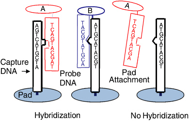
FIGURE 4-8 Principle of DNA-assisted pick and place. SOURCE: Esener, S. 2001. Emerging Applications of Micro and Nanophotonic Components and Their Interface with Biology. Briefing by Sadik Esener, Electrical and Computer Engineering Department, University of California San Diego, to the Committee on Implications of Emerging Micro and Nano Technology, National Academy of Sciences, Irvine, Calif., December 19.
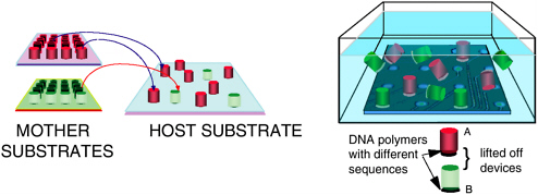
FIGURE 4-9 DNA-assisted microassembly. SOURCE: Esener, S. 2001. Emerging Applications of Micro and Nanophotonic Components and Their Interface with Biology. Briefing by Sadik Esener, Electrical and Computer Engineering Department, University of California San Diego, to the Committee on Implications of Emerging Micro and Nano Technology, National Academy of Sciences, Irvine, Calif., December 19.
devices and the host using small solder balls under the devices. After the hybridization process, the substrate is removed from the fluid and dried and the system is heat treated. Contacts are then formed in a manner similar to flip-chip bonding. Remaining DNA strands do not harm the quality of the ohmic contact. Although solder balls have been used in the initial demonstrations, many of the existing techniques for forming electrical contacts can in principle be used with DNA-assisted assembly.
This DNA-assisted assembly method is best suited to very small devices, on the order of 100 micrometers or less (all the way down to tens of nanometers), that can flow freely and find the correct position without blocking other devices.
In addition to DNA-assisted assembly, several other chemical and biological molecules can be used advantageously for device-forming pick-and-place as well as for micro- and nanoactuation. These techniques include, for example, the use of patterned hydrophobic films on hydrophilic substrates to form devices such as microfluidics and microlenses53,54 (see Figure 4-10) and proteins for transport and actuation functions.
PACKAGING
The packaging of integrated circuits involves many complex but well developed technologies.55,56 The packaging field has evolved in response to two major influences—cost and the need to put chips ever closer together on printed circuit boards. Dual-inline packages first gave way to surface mount packages, and these are now being superseded by chip-scale packages. Flip-chip attachment of ICs to boards essentially mates the chip to the package. Hermetic sealing of ICs from the outside environment has been a standard requirement. With the exception of
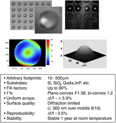
FIGURE 4-10 Lenslet array fabricated using hydrophobic/hydrophilic selectivity. SOURCE: Esener, S. 2001. Emerging Applications of Micro and Nanophotonic Components and Their Interface with Biology. Briefing by Sadik Esener, Electrical and Computer Engineering Department, University of California San Diego, to the Committee on Implications of Emerging Micro and Nano Technology, National Academy of Sciences, Irvine, Calif., December 19.
the windows on erasable, programmable read-only memories (EPROMs), IC packages have generally been opaque.
The packaging of MEMS devices is generally far more demanding than the packaging of ICs. The cost of packaging commonly represents 50 to 90 percent of the cost of a MEMS device. Many MEMS are in sealed packages. There are some cases in which ordinary microelectronic packages can be employed for MEMS. The primary instance is the packaging of inertial sensors, including both microaccelerometers and angular rate sensors. However, even MEMS devices in sealed packages often cannot use the same packages that have been developed for the IC industry. In fact, many MEMS have sealed packages that are significantly more complicated than standard electronic packages. Optical MEMS, which must have
windows, are the primary example. In the case of the digital mirror device from Texas Instruments, the window is large and its optical properties are demanding. MEMS switches for all-optical networks also have to have optical access to the moving device, either through windows or via optical fibers that penetrate the package, sometimes in large numbers. Other MEMS in sealed packages require a vacuum environment. Microresonators must have low losses to perform properly, so air must be excluded. Uncooled infrared sensor arrays, consisting of pixels thermally isolated from the substrate, also require vacuum packaging.
There are many MEMS that cannot be used in sealed packages. Pressure sensors are a commercially important example. They are generally sealed from the ambient atmosphere by an elastomer, which transmits pressure variations but excludes humidity and dirt. MEMS strain sensors sometimes have packages that are penetrated by an element that is attached to the piece being measured. Some MEMS, like chemical vapor sensors, must be in contact with the atmosphere to function. Sensors for the analysis of water, blood, and other liquids must also have access to the exterior environment. Maintaining the sensitivity of gas and liquid analyzers over long periods is challenging.
There are some MEMS that have no distinct packages because they are located on the surface of an object or in it. The microflaps that are being developed for the control of aircraft and the microthrusters for steering aircraft or spacecraft are examples. Here also, the needed interaction between the MEMS devices and the surroundings can be problematic. Dirt and rain in the atmosphere and particles and ions in low Earth orbit all challenge the long-term use of distributed MEMS on aerospacecraft.
It is likely that the packaging of sensors, actuators, and systems based on nanotechnology will prove as varied and challenging as the packaging of MEMS devices and systems. Very small devices can be inserted into living tissue without packages. Quantum dots can be inserted into living cells for a variety of purposes. Already, their fluorescence is being used as tags for specific molecules in cells. The coating of foreign objects within living organisms by biological processes is a difficult issue that must be solved before long-term use of these technologies can be considered.
RELIABILITY AND MANUFACTURABILITY
Initially, both the yield and the reliability of nanoproducts are expected to be low. Because of the scarcity of data made available for reliability analysis, extensive burn-in testing will be needed to screen out the early failures among newly designed and manufactured products. Optimal physical conditions for reliability testing of nanoproducts must be carefully investigated until the correlation of these conditions with failure mechanisms is better understood. It is also critical to use engineering experience to predict and to improve the future batch manufacturing processors using Bayesian statistics. The tremendous experience gained in
microelectronics manufacturing will be useful for the generation of nanoproducts as well.
Bayesian analysis is an efficient way of adjusting to shorter-loop manufacturing cycles. Using information available for similar systems, nonparametric Bayesian models can be used to transfer knowledge gained from one generation of models to the next generation.57 This method can also aid in the modification and adjustment of fabrication and processes for nanotechnology. Also, burn-in can effectively improve product reliability and enhance product yield.58
New Techniques for Reliability Improvement
From a manufacturing standpoint, process technologies for deep-submicron devices (<0.13 micrometer) are approaching physical limits. It is difficult to achieve high performance, high packing density, and high reliability. This manufacturing process requires a high initial investment and is very expensive to operate. Thus, cost reduction by developing new techniques or approaches becomes urgent. From a reliability point of view, accelerated life test and end-of-line failure analysis become less reliable as the chip shrinks and the devices become more complex. The simple failure analysis method of sampling the output of a manufacturing line must give way to new methods in order to better understand and control the input variables at each point in the manufacturing process.
The requirement of new techniques leads to the development of built-in reliability, wafer-level reliability (WLR), and qualified manufacturing line (QML) approaches.59 In the WLR approach, both processes and designs affect reliability. Since the traditional reliability approaches may not support enough test time or test parts to resolve failure rates as low as 10 FITs (1 FIT = 1 failure per 109 device-hours), considered the goal for failure rate, approaches for improving reliability and yield of any manufacturing process must be proactive rather than reactive. Based on the knowledge that anomalous material is generally produced by interactions between different process variables, proactive reliability control reduces process variation and eliminates some of the failures that might occur in the future. Table 4-1 shows some important shifts of the reliability paradigm from traditional to new techniques.
For other issues surrounding CAD/CAM/CAPP systems, burn-in, life-cycle approach, and manufacturing yield and reliability, see Appendix A.
Manufacturing Yield and Reliability
In the past, most attempts to assure high IC reliability used product testing, life testing, or accelerated stress tests of the entire circuit. Because this approach to product testing is getting more expensive, more time consuming, and less able to identify the causes of parametric and functional failures of ICs, new approaches
TABLE 4-1 Reliability Paradigm for Nanoproducts
|
Item |
Traditional Techniques |
New Techniques |
|
Approach |
Reactive |
Proactive |
|
Test methodology |
Output |
Input |
|
Failure mode |
Separated |
Integrated |
|
Emphasis |
Quality |
Reliability |
are needed. These new approaches make it possible to eliminate wear-out failures due to operational life.
There is a strong correlation between the number of field and life test failures and the manufacturing yield.60,61 Kuper et al.62 and van der Pol et al.63 present models for the yield-reliability relation and experimental data to show the correlation. Thus, the root causes of reliability failures are the same as those of yield failures, and the manufacturing yield depends on the number of defects found during the manufacturing process, which in turn determines reliability.
The degree of manufacturing success is measured by yield, which is defined as the average ratio of devices on a wafer that pass the tests to the total number of devices on the wafer. Since the yield is a statistical parameter and implies a probability function, yield functions are multiplied to attain the total yield. The total wafer yield is a measure of good chips per wafer normalized by the number of chip sites per wafer. Generally, since yields can be measured in various ways, the overall yield is calculated as the product of elements of yield, such as the line yield, the wafer probe yield, the assembly yield, the final test yield, and the burn-in yield.
Parameters that affect yield and defects, and the number of defects produced during the manufacturing process can be effectively controlled by introducing testing at critical processing steps rather than throughout the assembly line.64 This not only improves the reliability of the outgoing product but also significantly enhances the yield of the manufacturing process, thus increasing the quality of the overall system. Test points are effective only at critical processing steps, and their random distribution in the process was observed not to yield the desired results of high quality and minimal defects density. There is another way to control the yield. Since IC device yields are a function not only of chip area but also of circuit design and layout,65,66 it is possible to control and manage the yield of ICs by determining the probabilities of failure and critical areas for different defect types.
COMMERCIALIZATION
Commercialization of a diverse set of products using a new technology is not the same as the commercialization of a new product. Many treatises have discussed the barriers to the commercialization of new products in great detail. For
example, The Innovator’s Dilemma67 is an excellent text that analyzes the problems of bringing new technologies to bear on existing industries and the new commercial products that result.
The commercialization of a new technology that spans many different product categories, however, is an entirely different situation. Here, the issue is the use (presumably in multiple, diverse products and by multiple, diverse companies) of a particular set of manufacturing techniques that define the new technology. There are at least four prerequisites for effective commercialization of a new technology:
-
Identification of existing products that will benefit from the new technology or of possibilities for creating new ones.
-
Wide access to the technical details of the new technology.
-
Enlightened corporate management.
-
Sufficient reduction in product cost.
Identification of Products Manufactured in the New Technology
The identification of existing products that will benefit from the new technology or the creation of new products is an essential step in the acceptance and commercialization of a new manufacturing technology. Government can help industry meet this challenge, but only to the modest extent that the typically small government market can demand new products using the technology.
Wide Access to the Technical Details of the New Technology
The technical details of the new technology must be widely available so that a significant number of individuals are intimately acquainted with it or else the technology will never be developed. Initially, the only people familiar with the new technology are the research staff. A specific and deliberate effort must be made to transfer the expertise from research to product design. Expecting the design engineering community to discover and read the papers published by the research community is unrealistic. In the 1960s, the federal government, as the largest single customer for electronics, drove the migration in electronics, allowing companies to develop design engineering expertise at government expense (see Chapter 5). In today’s climate, the government will purchase only a small fraction of the devices made possible by micro- and nanotechnology. Further, many high-technology companies are financially strained by small margins. It thus behooves the government to find a way to drive the education of the design engineering community in micro- and nanotechnology in order to guarantee that industry truly does benefit from the federal research investment.
Enlightened Corporate Management
Enlightened corporate management willing to embrace the new technology is a key accelerator. This is not, per se, a government issue. However, government programs can create the knowledge base and make available infrastructure that increases awareness of the possibilities of a new technology and lowers the barriers to early product development. An example is the MOSIS project (see Box 4-1) and DoD’s role in the development of electronics. The DoD funded both research in new electronic technology and a foundry for making that new technology accessible to industry, government, and academia. MOSIS was a project funded to bring CMOS to as wide a community as possible by providing inexpensive, very-small-lot prototyping services. Few realize that Bill Joy used MOSIS68 to fabricate a prototype processor as one of his efforts to help launch a then infant start-up, Sun Microsystems.
Sufficient Reduction in Product Cost
A significant investment of corporate resources usually must be made to climb the learning curve and drive down manufacturing costs. Although most of the responsibility for this critical step falls on industry, government can play a strong role by maintaining critical-mass investments in the refinement of the new manufacturing technology. This is precisely the history of CMOS. Once sufficient industrial interest in CMOS had been developed by the MOSIS program, individual companies developed their own versions of CMOS that had superior performance, better reliability, and lower cost than MOSIS CMOS.
Government Role in Providing Wide Access to New Technology
One excellent example of a successful government program that gives the design engineering community wide access to new microtechnology (in this case, MEMS) is the MEMS Exchange offered by the Center for National Research Initiatives and supported by DARPA.
The MEMS Exchange is a distributed foundry service for MEMS, funded in part by DARPA since 1998. Currently the MEMS Exchange offers nearly 800 processes from 22 independent fabrication sites around the country. Over 1,250 MEMS designers from nearly 200 business, academic, and government organizations access the MEMS Exchange for their fabrication needs. This program stands as an example of how government funding can create access to the technical details of a new technology.
The overall goals were to provide designers with a maximum of process and design freedom, with quick turnaround time, and with high-quality prototyping. To achieve these goals, a distributed MEMS processing environment composed
|
BOX 4-1 MOSIS The Metal Oxide Semiconductor Implementation Service (MOSIS) was established in 1981 as a low-cost prototyping and small-volume production service for VLSI circuit development. MOSIS accepts designs from commercial firms, government agencies, and research and educational institutions around the world. It integrates user designs for a common process onto a single mask set, supplies the mask set to commercial foundries for fabrication, dices the finished wafers, and ships the individual dies to their corresponding requestors. This approach spreads the mask-making and fabrication costs among many users to make cost-effective fabrication of prototype chips possible. A single mask set can cost $50,000 and up, depending on the minimum line feature size and number of layers required. A 2.2-mm-square “tiny chip” fabricated using a 1.5-micrometer CMOS process costs only $1,080 for five copies. This low-cost fabrication service is ideal for students and researchers who need only a few copies of a given design or need to verify their designs before they enter mass production. MOSIS stimulates creativity in semiconductor circuit design and in related fields such as CMOS-compatible MEMS by offering a low-cost prototyping service. Figure 4-1-1 shows a sample detector die for a nano/picosatellite sun sensor fabricated as a “tiny chip.” MOSIS currently offers CMOS fabrication with 1.5-, 0.5-, 0.35-, 0.25-, and 0.18-micron processes from various vendors, 0.5- and 0.25-micron SiGe BiCMOS processes, a 0.5-micron silicon-on-insulator process, and a 0.2-micron GaAs process. See <http://www.mosis.org> for more information.  FIGURE 4-1-1 Two-dimensional active pixel sensor array. Photograph courtesy of the Aerospace Corporation. |
of a number of separate fabrication sites organized in a fabrication network and made available to the community through a central organization, the MEMS Exchange, was organized. An important and unique element is that designers can have the process sequence for their devices conducted at multiple fabrication sites. This approach affords designers with an enormous range of choices in processing techniques and materials as well as the ability to fully customize the processing sequence.
Figure 4-11 shows the rapid growth in user accounts for the MEMS Exchange. Furthermore, over the past 3 years, distributed, multiple-site MEMS device fabrication has been shown not only to be feasible but also to produce advanced and complex prototype devices with distinct advantages over those made at a single foundry. In the last 2 years, nearly 400 process sequence runs were successfully performed in the MEMS Exchange network for designers around the country, each run being different and customized for a particular application. Most of the process sequences delivered by the MEMS Exchange were performed at two sites, with a surprising number of runs having had processing work performed at three or more sites. The designers accessing the MEMS
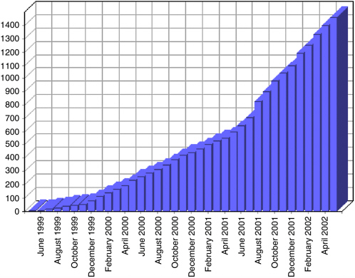
FIGURE 4-11 Cumulative user accounts for the MEMS exchange. Courtesy of the MEMS Exchange.
Exchange come from a wide range of organizations, including commercial (40 percent), academic (40 percent), and government laboratories (20 percent).
Fabrication sites enlisted in the MEMS Exchange include the University of California at Berkeley; Stanford University; Cornell University; the University of Michigan; Case Western Reserve University; Louisiana State University; the University of Illinois; Sony Semiconductor; Integrated Sensing Systems Corporation; Lance Goddard Associates; Microwave Bonding Corporation; Teledyne Electronics Corporation; Advanced MEMS Optical; Tactical Fabs, Inc.; Analog Devices; ASML; Zygo Teraoptics; Intelligent Micropatterning; Axsun Technologies; Aspen Technologies; Fiberlead, Inc.; and American Precision Dicing. Through these 22 fabrication sites that belong to the MEMS exchange, an extremely wide range of MEMS fabrication resources are available to the community, and new process capabilities are being added each week.
Effect of Manufacturing Complexity on Commercialization
Government-sponsored technology foundry programs (such as MOSIS, the Microelectronics Center of North Carolina, and the MEMS Exchange) have been successful in providing some level of technology access to the broader community, although demand for the services usually far outstrips capacity. However successful these programs may be in providing wide access to a technology, the cost barriers to the adoption of a new technology can only be solved by industry. Thus, government must make sure to involve industry in the new technology as soon as possible.
Manufacturing complexity strongly affects manufacturing cost. Thus, for technologies such as MEMS, cost depends on device complexity—in effect, how much integration between IC electronics and micromechanics has been accomplished. The three levels of manufacturing complexity of MEMS are these:
-
all micromechanics and no IC electronics
-
multichip modules or other assembled hybrids
-
integrated micromechanics and IC electronics
Commercialization has already occurred for MEMS on all three levels of complexity.
The third level is the most complicated and requires the most fabrication sophistication from industry. This level, in turn, can be subdivided into three specialties:
-
preprocessed micromechanics, postprocessed IC electronics
-
integrated micromechanics and IC electronics
-
postprocessed micromechanics, preprocessed IC electronics
Case Study: Texas Instruments and the Digital Mirror Device
Commercialization does not necessarily happen earliest for the simplest forms of manufactured MEMS (either those containing no IC electronics or hybrids of micromechanics and IC electronics). As an example of how one of the more difficult manufacturing processes (integrated micromechanics and IC electronics) was used for MEMS commercialization, the story of the Texas Instruments (TI) digital mirror device [DMD™] is related below. It shows that even after DMD feasibility had been demonstrated in the late 1980s, the commercialization effort required more than two decades to achieve profitability. This effort took place before the advent of government programs to lower the barriers to commercialization of MEMS. The cost of the DMD and the associated projector, called the digital light processor (DLP), is reported to have been nearly a billion dollars. Other commercialization efforts, most notably the MEMS airbag crash detection accelerometer, manufactured by Analog Devices, Inc. (ADI) had similar difficulties, but commercialization was accomplished at much lower cost and in a shorter time. This was primarily due to the relatively simpler structures ADI had to fabricate but also to the influx of engineers trained in MEMS in government programs.
TI was a pioneering company, well in advance of the technology curve, and was forced to solve many newly discovered MEMS problems entirely on its own. For micro- and nanotechnology to be commercialized quickly, it will be necessary for government not only to continue pursuing research in these technologies but also to guarantee wide access to them through programs specially funded for this purpose. The government must ask itself, first, if it really can expect most companies to be persistent in the face of product development adversity and, second, if it can wait so long for the new products to arrive.
TI’s DMD, shown in Figures 4-12 and 4-13, consists of an array of a half million or more mirrors that can electrically switch light to a working area. Figure 4-12 shows a cut-away of the DMD structural model. Figure 4-13 shows a photomicrograph of the DMD. The levels labeled on the photomicrograph are identified in Table 4-2 illustrating the complexity of the DMD, with seven functions squeezed into three levels.
The original DMD started out as an array of polymer film mirrors originated by a National Security Agency research group whose mission was optical correlation processing. Under DARPA support the mirror array technology was transferred to TI for development. Each mirror had to have a charge placed under the membrane to cause deflection and thus the enable the parallel correlation operations. This called for a large array of semiconductor circuits to enable the deflection. Feasibility was demonstrated, but manufacturing problems—for example, those from dust particles under the membrane causing defective mirror pixels— quickly emerged.
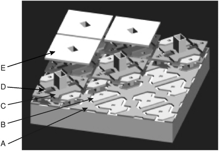
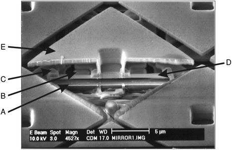
TABLE 4-2 High Complexity of the Digital Mirror Device
|
Label |
DMD Level |
Function |
|
A |
Electrode |
Bias Electrode |
|
B |
Electrode |
Address Electrode |
|
C |
Hinge/Beam |
Beam and Hinge Posts |
|
D |
Hinge/Beam |
Hinges |
|
E |
Mirror |
Mirror and Mirror Support Post |
A monolithic mirror approach using an array of aluminum alloy mirrors was developed to overcome the particle problems of the polymer mirrors. The aluminum mirrors worked much better in regard to dust but rapidly failed in operation because of the stress inherent in the mirror layer after plasma etching. Also, the TI printer division interested in the printer application fell on hard times, so the continuation of the program was always in doubt.
New DARPA money was supplied, administered by the Air Force. DARPA was then interested in large projection displays. During the 1990s development problems continued. (For instance, in operation, the mirrors would stick permanently to the underlying films; the mirrors did not optimally fill the optical aperture, leading to a checkerboard display image; there was high optical insertion loss from a mismatch in the pixel size and the size of the arc lamp; a very high light flux on the DMD was required; arc lamp longevity was insufficient; and the cost of engineering of a small sophisticated light handling system, including an optically flat window on the package top, was high.) By the late 1980s the DMD was being touted as a MEMS success story, but these manufacturability issues continued to threaten the viability of commercialization.
During the 1990s, TI, using its own funds, gradually worked out solutions to the DMD manufacturability problems. Mirror reliability was solved with a hidden mirror hinge made out of an amorphous material. Since there were no grain boundaries in the hinge, there were no sources of the cracks that had led to high failure rates in the metal hinges. Stiction was fixed by fabricating springs and a fluorocarbon coating on the back side of the mirrors. The springs produced a restoring force when the mirror touched the base layer. The hidden-hinge design allowed for a more optically efficient pixel, filling the aperture. Obtaining a robust, very bright light source turned out to be an enormous problem, and the light source is still a major cost component in the DMD system.
One of the veteran engineers on the project at Texas Instruments, Michael Mignardi, recently gave an IEEE seminar detailing the scale of TI’s effort to successfully produce the DMD.69 Even after feasibility had been demonstrated in the late 1980s, it took another 10 years to reach profitability, with the effort being spread roughly equally among device improvement, packaging, and testing. Low outgasing adhesives were used to prevent the buildup of a sticky layer inside the package, which would result in stiction problems. A zeolite getter was included
in the package to mitigate water-induced stiction in the completed package. These and other innovations led to TI turning its first profit on projectors in 2000.
Specifications for a 1.2-million-pixel projector device include mirrors that tilt 10 to 12 degrees to deflect light onto a screen. Only five stuck-on pixels are permitted for a shipped DMD. Clearly, achieving this level of yield and reliability required an enormous effort in developing test equipment and lifetime testing for the semiconductor layer, the mirror level, and the combined levels in action.
TI and its technological team deserve a special place in the MEMS Hall of Fame for their perseverance in bringing the projector product to market. The Air Force also deserves credit for early support. Most importantly the development of the successful DMD back-end processing indicates that such processing can be solved by a determined team, even for very complex devices and systems. But it also illustrates the very real difficulties in turning a laboratory demonstration into a reliable product—difficulties that will undoubtedly confront all emerging micro- and nanotechnology applications in as yet unanticipated ways.
New technologies are generally thought to become profitable after 10 years. It is generally believed that so far few, if any, MEMS projects have become profitable long-term. All of which is to say that building micro- and nanotechnology materials and systems is very difficult. Continuing to approach these technologies in the cottage industry mode that is currently fashionable will not produce DMD-type successes. There is a need for farsighted management and technical staffs—and for deep pockets. Further, the multidisciplinary research capacity that TI had available does not exist in many of today’s companies in the face of the increased pressure for short-term profitability, and it certainly is not possible in the small-company entrepreneurial environment that is attempting to bring nanotechnology to fruition.
FINDINGS AND RECOMMENDATIONS
Finding 4-1. Lithography and pattern transfer and self-assembly are key enablers for evolving micro- and nanotechnologies.
Recommendation 4-1. The AFRL R&D program will require access to micro- and nanolithography and pattern transfer tools. This should be accomplished using available national facilities or otherwise providing the function internally. Research into new nanolithography and patterning technologies, complementary to the industry push for high-throughput tools, would be a worthwhile investment. The Air Force should not compete with industry efforts, particularly in silicon technology, but should concentrate on developing processes for structures and materials that are outside traditional silicon processing—for example, deep etching for MEMS and integration of new materials with silicon.
Finding T7. Integration of micro- and nanoscale processes and of different material systems will be broadly important for materials, devices, and packaging. Self-assembly and directed assembly of dissimilar elements will be necessary to maximize the functionality of many micro- and nanoscale structures, devices, and systems. Achievement of high yields and long-term reliability, comparable to those of the current integrated circuit industry, will be a major challenge.
Recommendation T7. The Air Force should monitor progress in self- and directed-assembly research and selectively invest its R&D resources. It will be critical for the Air Force to participate in developing manufacturing processes that result in reliable systems in technology areas where the military is the dominant customer—for example, in sensors and propulsion systems. Developments in many of these areas will be driven by the commercial sector. The Air Force must stay aware of advances and apply them to its unique needs. As an example, in sensor applications a wide range of otherwise incompatible materials and fabrication processes is likely to be necessary.
Finding 4-2. So much is already known about progress in silicon, with its already highly developed and constantly improving manufacturing processes, that it is unlikely a sui generis technology will spring up sufficiently developed and robust that it will immediately supplant not only the transistor but also all the rest of the integrated circuit. Integrated circuit technology has become extremely sophisticated, and the industry is devoting extensive resources to extending this sophistication in its drive to validate Moore’s law for future IC generations. In contrast, nanotechnology is at a much earlier development stage, concentrating on the behavior of individual devices and circuit components (switches, wires, etc.). It is most likely that these new technologies will first find use as complements to silicon, not as immediate replacements for integrated circuits. Over the longer term, it is not possible to predict the relative roles of integrated circuits and new and evolving nanotechnologies.
Recommendation 4-2. The Air Force should emphasize those areas of micro- and nanotechnology for information processing that are potentially integrable with silicon technology and that address Air Force-specific, non-commercial military applications.
Finding 4-3. The path from laboratory demonstration to the manufacture of reliable devices and systems is long and arduous, requiring extensive resources and prodigious technology development. This will undoubtedly be as true of today’s emerging technologies as it has been throughout the history
of technology. It is worthwhile to consider this lesson when listening to the siren songs appearing daily, particularly in the popular and business press, on the future benefits of nanotechnology. There is undoubtedly an exciting future, and just as undoubtedly, we will find many surprises, both positive and negative, along the way.
Recommendation 4-3. Air Force research efforts should be directed not only to the science of micro- and nanotechnology, but also to the development of devices and systems and wide access to the manufacturing technology required to produce them.
REFERENCES
1. Nagel, D.J. 2002. Technologies for micrometer and nanometer pattern and material transfer. Pp. 557–701 in Direct-Write Technologies for Rapid Prototyping Applications: Sensors, Electronics, and Integrated Power Sources. A. Pique and D.B. Chrisey, eds. New York, N.Y.: Academic Press.
2. Bjorkholm, J.E. 1998. EUV lithography–the successor to optical lithography? Available online at <http://www.intel.com/technology/itj/q31998/articles/art_4.htm> [July 8, 2002].
3. Smith, H.I. 2001. Japan could dominate industry with x-ray lithography. Available online at <http://www.e-insite.net/semiconductor/index.asp?layout=article&articleId=CA61809&stt=001> [July 8, 2002].
4. Institut für Mikrotechnik Mainz. 2001. LIGA Technology. Available online at <http://www.imm-mainz.de/> [July 8, 2002].
5. Chou, S.Y., L. Zhuang, and L.J. Guo. 1999. Lithographically induced self-construction of polymer microstructures for resistless patterning. Applied Physics Letters 75(7): 1004–1006.
6. Chou, S.Y., and L. Zhuang. 1999. Lithographically induced self-assembly of periodic polymer micropillar arrays. Journal of Vacuum Science Technology B 17(6): 3197–3202.
7. Becker, H., and U. Heim. 1999. Silicon as tool material for polymer hot embossing. Pp. 228– 231 in Proceedings of MEMS ’99: The 12th IEEE International Conference on Micro Electro Mechanical Systems. New York, N.Y.: IEEE.
8. Glinsner, T. 2001. Nanoimprinting can solve pattern-generation problems. R&D Magazine 43(7): 33.
9. Chou, S.Y., P.R. Krause, and P.J. Renstrom. 1995. Imprint of sub-25 nm vias and trenches in polymers. Applied Physics Letters 67(21): 3114–3116.
10. Chou, S.Y. 2001. Nanoimprint lithography. Available online at <http://www.ee.princeton.edu/~chouweb/newproject/page3.html> [July 8, 2002].
11. Johnson, S.C. 1999. Selective Compliant Orientation Stages for Imprint Lithography. Available online at <http://sfil.org/research/papers/sjthesis.pdf> [July 8, 2002].
12. Xia, Y., and G.M. Whitesides. 1998. Soft lithography. Annual Review of Materials Science 28: 153–184.
13. Senturia, S.D. 2001. Microsystem Design. Boston, Mass.: Kluwer Academic Publishers.
14. Kauffman, S.A. 1995. At Home in the Universe: The Search for Laws of Self-Organization and Complexity. New York, N.Y.: Oxford University Press.
15. This series, for example, provides a good overview of the topic: Lehn, J.M., J.L. Atwood, J.E.D. Davis, D.D. MacNicol, and F. Vögtle. 1996. Comprehensive Supramolecular Chemistry, Vols. 1–11. New York, N.Y.: Pergamon.
16. Lehn, J.M. 1995. Supramolecular Chemistry: Concepts and Perspectives. New York, N.Y.: VCH Press.
17. Balzani, V., and L. DeCola. 1992. Supramolecular Chemistry. Dordrecht, The Netherlands: Kluwer Academic Press.
18. Desiraju., G.R. 1996. The Crystal as Supramolecular Entity: Perspectives in Supramolecular Chemistry, Volume 2. New York, N.Y.: John Wiley & Sons.
19. Desiraju, G.R. 1989. Crystal Engineering: The Design of Organic Solids. New York, N.Y.: Elsevier.
20. Manne, S., and G.G. Warr. 1999. Supramolecular Structure in Confined Geometries. Washington, D.C.: American Chemical Society.
21. Jones, M.N., and D. Chapman. 1995. Micelles, Monolayers and Biomembranes. New York, N.Y.: Wiley-Liss.
22. Wilcoxon, J.P., J.E. Martin, and D.W. Schaefer. 1989. Aggregation in colloidal gold. Physical Review A 39(5): 2675–2688.
23. Kumar, A., N.L. Abbott, E. Kim, H.A. Biebuyck, and G.M. Whitesides. 1995. Patterned self-assembled monolayers and mesoscale phenomena. Accounts of Chemical Research 28(5): 219– 226.
24. De Gennes, P.G., and J. Prost. 1993. The Physics of Liquid Crystals, 2nd Ed. New York, N.Y.: Oxford University Press.
25. Rouvray, D. 2000. Molecular self-assembly. Chemistry in Britain 36(7): 26–29.
26. Huc, I., and J.M. Lehn. 1997. Virtual combinatorial libraries: Dynamic generation of molecular and supramolecular diversity by self-assembly. Proceedings of the National Academy of Sciences 94(6): 2106–2110.
27. Frechet, J.M.J. 2002. Dendrimers and supramolecular chemistry. Proceedings of the National Academy of Sciences 99(8): 4782–4787
28. Whitesides, G.M., and J.C. Love. 2001. The art of building small—Researchers are discovering cheap, efficient ways to make structures only a few billionths of a meter across. Scientific American 285(3): 38–47.
29. Van Hest, J.C.M., and D.A. Tirrell. 2001. Protein-based materials: Toward a new level of structural control. Chemical Communications (19): 1897–1904.
30. Yu, S.J.M., C.M. Soto, and D.A. Tirrell. 2000. Nanometer-scale smectic ordering of genetically engineered rodlike polymers: Synthesis and characterization of monodisperse derivatives of poly (g-benzyl a, L-glutamate). Journal of the American Chemical Society 122(28): 6552– 6559, and references therein.
31. Limberis, L., and R.J. Stewart. 2000. Toward kinesin-powered microdevices. Nanotechnology 11(2): 47–51.
32. Srinivasarao, M. 1999. Nano-optics in the biological world: Beetles, butterflies, birds, and moths. Chemical Reviews 99(7): 1935–1961.
33. Miller, J.S., and A.J. Epstein. 2000. Molecule-based magnets—An overview. MRS Bulletin 25(11): 21–28.
34. Ovcharenko, V.I., and R.Z. Sagdeev. 1999. Molecular ferromagnets. Russian Chemical Reviews 68(5): 345–363.
35. Alivisatos, A.P. 2001. Less is more in medicine—Sophisticated forms of nanotechnology will find some of their first real-world applications in biomedical research, disease diagnosis, and, possibly, therapy. Scientific American 285(3): 67–73.
36. Hooks, D.E., T. Fritz, and M.D. Ward. 2001. Epitaxy and molecular organization on solid substrates. Advanced Materials 13(4): 227–241, and references therein.
37. Choquette, K.D., K.L. Lear, R.P. Schneider, K.M. Geib, J.J. Figiel, and R. Hull. 1995. Fabrication and performance of selectively oxidized vertical-cavity lasers. IEEE Photonics Technology Letters 7(11): 1237–1239.
38. Hatzor, A., and P.S. Weiss. 2001. Molecular rulers for scaling down nanostructures. Science 291(5506): 1019–1020.
39. For a contemporaneous snapshot of this field, see, for example, Fan, J.C.C., and J.M. Poate. 1986. Heteroepitaxy on Silicon. Materials Research Society Symposia Proceedings 67. Pittsburgh, Pa.: Materials Research Society.
40. Kapon, E., D.M. Hwang, and R. Bhat. 1989. Stimulated-emission in semiconductor quantum wire heterostructures. Physical Review Letters 63(4): 430–433.
41. Zhou, Y.X., S. Luong, C.P. Hains, and J. Cheng. 1998. Oxide-confined monolithic, multiple-wavelength vertical-cavity surface-emitting laser arrays with a 40-nm wavelength span. IEEE Photonics Technology Letters 10(11): 1527–1529.
42. For a recent survey, see the special section on the growth of heterostructure materials on nanoscale substrates, S.D. Hersee, D.A. Zubia and S.R.J. Brueck, eds. 2002. IEEE Journal of Quantum Electronics 38(8).
43. Cui, Y. and C.M. Lieber. 2001. Functional nanoscale electronic devices assembled using silicon nanowire building blocks. Science: 291(5505): 851–853.
44. Duan, X.F., Y. Huang, Y. Cui, J.F. Wang, and C.M. Lieber. 2001. Indium phosphide nanowires as building blocks for nanoscale electronic and optoelectronic devices. Nature 409(6816): 66– 69.
45. Gudiksen, M.S., L.J. Lauhon, J. Wang, D.C. Smith, and C.M. Lieber. 2002. Growth of nanowire superlattice structures for photonics and electronics. Nature 415(6872): 617–620.
46. International Technology Roadmap for Semiconductors. 2001. Available online at <http://public.itrs.net/> [July 3, 2002].
47. Moravec, H. 1998. When will computer hardware match the human brain? Available online at <http://www.transhumanist.com/volume1/moravec.htm> [July 8, 2002].
48. Talghader, J.J., J.K. Tu, and J.S. Smith. 1995. Integration of fluidically self-assembled optoelectronic devices using a silicon-based process. IEEE Photonics Technology Letters 7(11): 1321–1323.
49. Esener, S.C., D. Hartmann, M.J. Heller, and J.M. Cable. 1998. DNA-assisted microassembly: A heterogeneous integration technology for optoelectronics. Paper # CR70-07 in Heterogeneous Integration: Systems on a Chip, Proceedings of SPIE, Volume CR70. A. Husain and M. Fallahi, eds. Bellingham, Wash.: The International Society for Optical Engineering.
50. Hartmann, D.M., M. Heller, S.C. Esener, D. Schwartz, and G. Tu. 2002. Selective DNA attachment of micro- and nanoscale particles to substrates. Journal of Materials Research 17(2): 473– 478.
51. Ozkan, M., C.S. Ozkan, O. Kibar, and S.C. Esener. 2000. Massively parallel low-cost pick-and-place of optoelectronic devices by electrochemical fluidic processing. Optics Letters 25(17): 1285–1287.
52. Ozkan, M., C.S. Ozkan, O. Kibar, M.M. Wang, S. Bhatia, and S.C. Esener. 2001. Heterogeneous integration through electrokinetic movement. IEEE Engineering in Medicine and Biology Magazine 20(6): 144–151.
53. Hartmann, D.M., O. Kibar, and S.C. Esener. 2001. Optimization and theoretical modeling of polymer microlens arrays fabricated using the hydrophobic effect. Applied Optics 40(16): 2736– 2746.
54. Hartmann, D.M., D.J. Reiley, and S.C. Esener. 2001. Microlenses self-aligned to optical fibers fabricated using the hydrophobic effect. IEEE Photonics Technology Letters 13(10): 1088– 1090.
55. Harper, C.A. 2000. Electronic Packaging and Interconnection Handbook, Third Edition. New York, N.Y.: McGraw-Hill.
56. Gilleo, K. 2002. Area Array Packaging Handbook. New York, N.Y.: McGraw-Hill.
57. Kuo, W., W.T.K. Chien, and T. Kim. 1998. Reliability, Yield, and Stress Burn-In: A Unified Approach for Microelectronics Systems Manufacturing and Software Development. Boston, Mass.: Kluwer Academic Publishers.
58. Kim, T., W. Kuo, and W.T.K. Chien. 2000. Burn-in effect on yield. IEEE Transactions on Electronics Packaging Manufacturing 23(4): 293–299.
59. Shideler, J.A, T. Turner, J. Reedholm, and C. Messick. 1995. A systematic approach to wafer level reliability. Solid State Technology 38(3): 47–54.
60. Kim, T., W. Kuo, and W.T.K. Chien. 2000. Burn-in effect on yield. IEEE Transactions on Electronics Packaging Manufacturing 23(4): 293–299.
61. Kim, T. and W. Kuo. 1999. Modeling manufacturing yield and reliability. IEEE Transactions on Semiconductor Manufacturing 12(4): 485–492.
62. Kuper, F., J. van der Pol, E. Ooms, T. Johnson, R Wijburg, W. Koster, and D. Johnston. 1996. Relation between yield and reliability of integrated circuits: Experimental results and application to continuous early failure rate reduction programs. Pp. 17–21 in Proceedings of the 1996 34th Annual IEEE International Reliability Physics Symposium. New York, N.Y.: Institute of Electrical and Electronics Engineers.
63. Van der Pol, J., F. Kuper, and E. Ooms. 1993. Relation between yield and reliability of integrated circuits and application to failure rate assessment and reduction in the one digit fit and ppm reliability era. Microelectronics and Reliability 36(11/12): 1603–1610.
64. Shideler, J.A, T. Turner, J. Reedholm, and C. Messick. 1995. A systematic approach to wafer level reliability. Solid State Technology 38(3): 47–54.
65. Kuo, W., and T. Kim. 1999. An overview of manufacturing yield and reliability modeling for semiconductor products. Proceedings of the IEEE 87(8): 1329–1344.
66. Kim, T., and W. Kuo. 1999. Modeling manufacturing yield and reliability. IEEE Transactions on Semiconductor Manufacturing 12(4): 485–492.
67. Christensen, C.M. 2000. The Innovator’s Dilemma: When New Technologies Cause Great Firms to Fail. New York, N.Y.: HarperBusiness.
68. Personal Communication between Keith Uncapher, Dean Emeritus, University of Southern California, and Al Pisano, Committee on Implications of Emerging Micro and Nano Technologies, March 2001.
69. Mignardi, M. 2001. The Digital Micromirror Device: Its Fabrication and Use. Presentation by Michael Mignardi Texas Instruments, to the IEEE weekly seminar, Southern Methodist University, Dallas, Texas, November 27.


