
2
Expectations for Future Micro-and Nanotechnologies
OVERVIEW OF CURRENT STUDIES
Visions for the future of nanotechnology and for its impact on technology in general are many. In this chapter, the committee discusses three: the International Technology Roadmap for Semiconductors (ITRS), the MEMS Industry Group 2001 Annual Report, and the National Nanotechnology Initiative (NNI).
International Technology Roadmap for Semiconductors
In 1992, the Semiconductor Industry Association (SIA) published a roadmap that charted the future of the industry by providing consensus predictions of future requirements and suggested solutions to anticipated problems with a 15-year time horizon. The industry roadmapping has evolved into a continuous process, with major reissues every 2 years. The most recent full update, the 2001 ITRS1 includes input from semiconductor manufacturers worldwide and covers a 16-year period, divided into the near term (2001-2007) and the long term (2008-2016). Past SIA roadmaps have proven to be reliable predictors of future integrated circuit performance.
The growth in integrated circuit (IC) performance over the past 30 years has been both phenomenal and consistent. One performance measure, the number of transistors per chip, or per integrated circuit (see Figure 2-1), demonstrates the exponential growth predicted by Moore’s law. This exponential growth has been the result of continually shrinking the dimensions of integrated circuit elements from tens of micrometers to tens of nanometers. Figure 2-2 shows how this
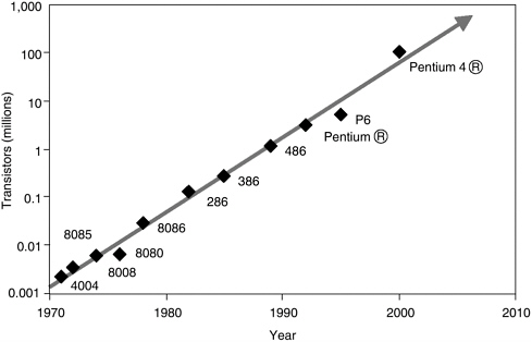
FIGURE 2-1 Integrated circuit growth. SOURCE: Adapted from Intel. 2002. Moore’s Law. Available online at <http://www.intel.com/research/silicon/mooreslaw.htm> [May 31, 2002].
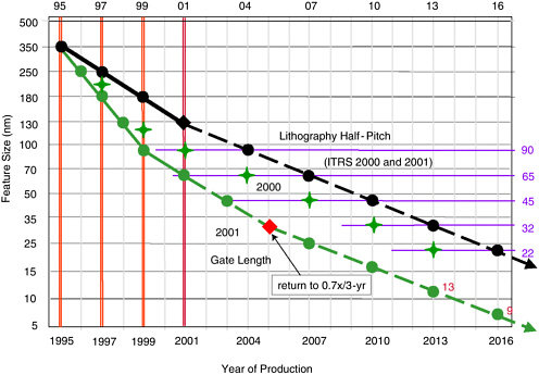
FIGURE 2-2 Lithography half-pitch feature size versus time. SOURCE: Adapted from the International Technology Roadmap for Semiconductors, 2001 edition. Austin, Tex.: International SEMATECH.
affects the minimum feature size (transistor gate length) required. Scaling has been employed to increase nearly all aspects of performance, including speed, power consumption per operation, and reliability. At the same time, the cost of the highest performance chips has remained approximately constant, and the cost per function has gone down dramatically, by over nine orders of magnitude.
The 2001 ITRS consists of target values for representative characteristics of circuits that are predicted to be in production each year from now until 2016. Examples include dynamic random-access memory (DRAM) half-pitch, multiprocessor unit gate length, and junction depth. The manufacturability of each characteristic quantity is evaluated and assigned to one of three categories: manufacturable, currently being optimized; manufacturable, solutions are known; and, manufacturing solutions are not known. A point in the future where several quantities in the roadmap fall into the “manufacturing solutions are not known” category signals trouble and is called a red-brick wall. For example, a brick wall currently exists in 2007, at the end of the near-term period, indicating that research breakthroughs will be required to maintain the predicted schedule. Both new materials and advanced metal oxide semiconductor field effect transistor (MOSFET) structures may be required to break through this red brick wall. The longer-term challenge is to develop a manufacturable non-classical MOSFET structure to extend the technology to and beyond the end of the roadmap.
Table 2-1 shows the predictions of the 2001 ITRS for a few selected parameters that are characteristic of DRAM and microprocessor technologies. If the roadmap is achieved, over the period of 2001 to 2016, we will see a 128-fold increase in memory at three-fourths the cost and a 32-fold increase in microprocessor functionality and a 17-fold increase in microprocessor speed at one-fifth the cost. These huge gains in storage, functionality, and speed, as we shall see later in this report, have important implications for the Air Force.
No clear path is seen for extending the technology beyond the roadmap horizon of 2016. Indeed, a transition to an alternative technology may be needed before 2016. The 2001 ITRS notes as follows:2
The horizon of the Roadmap challenges the most optimistic projections for continued scaling of CMOS (for example, MOSFET channel lengths of roughly 9 nm)...[and] it is difficult for] most people in the semiconductor industry to imagine how we could continue to afford the historic trends in process equipment and factory costs for another 15 years!
A new technology will be needed, because, beyond the numerous technological and economic difficulties arising with sub-10-nanometer minimum dimensions, MOSFET integrated circuit (IC) technologies cannot shrink indefinitely. Ultimately, the discrete atomic nature of matter limits the shrinkage. Before that, however, the quantum phenomena characteristic of nanotechnology become important, and scaling laws that have not taken such phenomena into account will prove problematical. For example, quantum mechanical tunneling of charge
TABLE 2-1 Predictions of 2001 ITRS for Selected Parameters
|
|
Year of Production |
|||||
|
Characteristic |
2001 |
2004 |
2007 |
2010 |
2013 |
2016 |
|
Memory |
||||||
|
DRAM feature size, ½ pitch (nm) |
130 |
90 |
65 |
45 |
32 |
22 |
|
Generation at production |
512M |
1G |
4G |
8G |
32G |
64G |
|
Cost/bit at production (packaged microcents) |
7.7 |
2.7 |
0.96 |
0.34 |
0.12 |
0.042 |
|
Logic |
||||||
|
Minimum feature size (physical gate length) (nm) |
65 |
37 |
25 |
18 |
13 |
9 |
|
Functions/chip (millions of transistors) |
276 |
553 |
1,106 |
2,212 |
4,424 |
8,848 |
|
Cost/transistor, high performance, at production (microcents) |
97 |
34 |
12 |
4.3 |
1.5 |
0.54 |
|
Local clock (MHz) |
1,684 |
3,990 |
6,739 |
11,511 |
19,348 |
28,751 |
|
Power dissipation, high performance (W) |
130 |
160 |
190 |
218 |
251 |
288 |
|
SOURCE: Adapted from the International Technology Roadmap for Semiconductors, 2001 edition. Austin, Tex.: International SEMATECH. |
||||||
carriers becomes significant at 10 nanometers and dominates below 3 nanometers. In addition, at a few nanometers, about 50 percent of all atoms in a particle are surface atoms, so that electrical properties are no longer determined by solid-state bulk phenomena.
On the other hand, the same nanoscale phenomena offer the opportunity to develop whole new classes of devices based on the principles of quantum physics, which may propel integrated circuits toward and beyond the end of the current roadmap. FlashRAM, now widely used to store data in digital cameras and MP3 music players, uses quantum-mechanical tunneling of electrons through ~10-nanometer-thick dielectric layers to charge a memory storage element. The ITRS (2001) and the European Commission Technology Roadmap for Nanoelectronics (2000)3 discuss a number of candidates for replacing classical CMOS. However, it may be that systems based on these new principles function in a manner significantly different from current computing systems and are more suited to alternative architectures. There is no established roadmap to the development of these technologies, even though one may speculate on their functionality. A possible path is illustrated in Figure 2-3.
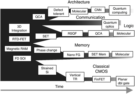
FIGURE 2-3 Possible roadmap. QCA, quantum cellular automata; CNN, cellular nonlinear networks; RTD–FET, resonant tunneling diode–field effect transistor; SET, single electron transistor; RSQF, rapid single quantum flux logic; nano FG, nano floating gate; SET mem, single electron transistor memory; FD SOI, fully depleted silicon on insulator; SI, silicon; vertical TR, vertical transistor; FinFET, a form of double gate transistor; planar dbl gate, planar double gate transistor. SOURCE: Adapted from the International Technology Roadmap for Semiconductors, 2001 edition. Austin, Tex.: International SEMATECH.
MEMS Industry Group 2001 Annual Report
The MEMS Industry Group is a nonprofit trade association of 22 member companies, established, in part, to “enable the exchange of non-proprietary information among members” and “provide reliable industry data that furthers the development of technology.” Its annual report for 2001 discusses the key drivers and challenges expected by the industry over the next 20 years.4 The committee briefly summarizes the findings here.
Starting with materials and fabrication approaches developed for the microelectronics industry, multiple miniaturized electronic and mechanical subsystems are integrated into a single microsystem. MEMS devices find applications in diverse industries because of their ability to perform complex functions and their
relatively low cost, small size, low weight, high reliability, and good performance. The MEMS industry was estimated in 2000 to be between $2 billion and $4 billion in size (contrasted with about $180 billion for the IC industry) with 1.6 MEMS devices per person in use in the United States in 2001 and a compound annual rate of growth of 45 percent. MEMS production in the United States is currently concentrated on sensors and telecommunications, but there is a strong trend toward diversification.
The MEMS Industry Group’s 2001 Annual Report foresees tremendous growth for the industry over the next 20 years. It discusses the expected roadmap for the industry in terms of the critical drivers and challenges expected, with driver defined as a force that “causes significant reactions in MEMS technology or commercialization.” The advent of wireless networks and communications are a major driver for the introduction of MEMS into information technology. Drivers for the application of MEMS in health care are our aging population and our strong concern for a high quality of life.
Technological drivers include the introduction of new materials, e.g., plastics and magnetic and biocompatible materials, into the MEMS repertoire. Biotechnological drivers will include cell handling and living organisms. Other technological drivers involve interfaces between systems at different length scales, the need for low power operation, and the dramatic increase in computing power. Higher-fidelity modeling is necessary to ensure first-pass success. On the fabrication side, technological drivers include the use of magnetic and plastic materials within the process. A technological driver anticipated in the long range is the creation of a single fabrication process usable in a variety of electronic applications. The use of MEMS in extreme environments and for biomedical applications will be technological drivers for MEMS packaging. All of these applications would benefit enormously from advances in MEMS-specific design, modeling, and simulation tools.
The report also discusses technology challenges—that is, the known barriers to future progress in MEMS development and applications. First, MEMS fabrication equipment manufacturers are seen as being too few in number and too limited in diversity and quality. Similar problems are seen in packaging equipment for MEMS. Second, there is a need for standard (as opposed to custom) foundry services to facilitate testing and characterization by MEMS producers. Third, a library of reusable circuit designs needs to be developed to provide interfaces with MEMS. Fourth, packaging methods specific to MEMS need to be developed, and their effect on performance needs to be quantified. Other near-and intermediate-term issues concern communication and the need for a suitably trained workforce, e.g., MEMS-trained circuit designers. Over the longer term, there will be technological challenges relating to the stacking, assembly, lithography, and processing of three-dimensional geometries and the greater integration of electronics with MEMS.
The National Nanotechnology Initiative
In September 1999, the President’s Interagency Working Group on Nanoscience, Engineering and Technology (IWGN) issued a report arguing that we were poised at a point of great scientific and technological opportunity. Science had gained a much greater appreciation of the degree to which controlling the structure of matter on the nanoscale could determine the macroscopic properties of materials. Further, major advances had been made in our ability to manipulate matter at the atomic and molecular levels. The working group report recommended the initiation of a national program in nanotechnology, which it defined as “the creation and utilization of materials, devices, and systems through the control of matter on the nanometer-length scale, that is, at the level of atoms, molecules and supramolecular structures.” Nanotechnology, it was said, “could impact the production of virtually every human-made object . . . and lead to the invention of objects yet to be imagined.”5
In July 2000, a national initiative in nanotechnology was proposed at a funding level of $225 million, an 83 percent increase in U.S. federally funded nanotechnology research in FY 2001. Congress approved a $152 million (+56 percent) increase in funding to support what is now known as the National Nanotechnology Initiative (NNI),6 bringing federal funding for nanotechnology to $422 million in FY 2001. U.S. federal spending for 2002 is currently estimated at $600 million, an increase of an additional 42 percent.
The NNI called for a coordination of nanotechnology efforts at the Department of Defense, the Department of Energy, the National Science Foundation, the National Institutes of Health, the National Institute of Standards and Technology, and the National Aeronautics and Space Administration. It established a series of Grand Challenges, whose success would make a substantial difference in the lives of the U.S. citizenry.
While nanotechnology is in its infancy and substantial changes in direction and emphasis can be expected in the research portfolio of the NNI over the next decade, an inspection of the current NNI Grand Challenges gives an overview of the initial intent. There are nine NNI Grand Challenges in all, which are briefly described below.
-
Nanostructured materials by design. By understanding the effect of a material’s nanostructure on its macroscopic properties and by developing new methods of fabrication and measurement, produce materials that are stronger, lighter, harder, self-repairing, smarter, and safer.
-
Nanoelectronics, optoelectronics, and magnetics. Develop new device concepts and methods of fabrication and processing. These new devices will be integrated into existing systems, and new architectures will be developed. Modeling and simulation of complex systems over a broad
-
range of lengths will be used. Explore the novel optical properties available with photonic bandgap structures.
-
Advanced health care, therapeutics, and diagnosis. Improve our health by developing new medical imaging techniques and biosensors; use nanoparticles to target the delivery of drugs directly to the most important sites; improve biological implants through nanoscale engineering of the implant-bone interface; develop devices to enable vision and hearing; produce better diagnostic methods using gene sequencing methods.
-
Nanoscale processes for environmental improvement. Develop a fundamental understanding of nanoscale processes important to maintaining environmental quality and controlling and minimizing unwanted emissions. Find methods to both measure pollutants and remove nanoscale pollutants from the water and air.
-
Efficient energy conversion and storage. Obtain more efficient sources of energy through improved nanocrystal catalysts, more efficient and color tunable solar cells, and efficient photoactive materials for solar conversion of molecules to fuels. Explore the potential of carbon nanotubes for high-density hydrogen storage and the use of fluids with suspended nanocrystalline particles to improve the efficiency of heat exchangers. Develop high-performance magnetic materials and devices using nanoscale, layered materials. Develop high-efficiency light sources using layered quantum well structures.
-
Microcraft space exploration and industrialization. Scale down the size of a spacecraft by an order of magnitude, allowing continuous exploration of space beyond the solar system. Utilize the high strength and light weight of nanostructured materials to greatly reduce fuel consumption, as well as permit the construction of large systems using inflatable structures, e.g., antennas. Enable sophisticated autonomous decision making through the development of nanoelectronics and nanomagnetics and the ability to store large amounts of data. Use self-repairing materials to further extend the reach of our exploration. Develop MEMS to allow for efficient control of optical surfaces and extend the development of radiation-tolerant technologies.
-
Bionanosensor devices for communicable disease and biological threat detection. Greatly improve both the detection of and response to threats from chemical or biological warfare and from human disease through advances in nanoscience and nanotechnology. Improve health and extend human capabilities using nanodevices. In vivo nanodevices will derive power from body chemistry in the same ways natural molecular motors function and will be able to detect disease or chemical or biological threats. These nanodevices will also be capable of counteracting the threats of bioterrorism and chemical warfare. Perform critical research on issues relating to the compatibility between nanodevice materials and
-
living tissue. Microfluidics and sensor fouling will be important research areas.
-
Application to economical and safe transportation. Develop more efficient means of transportation based on nanomaterials to provide lighter materials with lower failure rates; more durable materials for roads and bridges; smart materials that detect impending failure and carry out self-repair; low-friction and low-corrosion coatings; performance and emissions sensors; and emissions traps.
-
National security. Use nanoscience and technology to assure military dominance at reduced cost and manpower, yet with lower risk to war fighters. Produce enormous gains in knowledge superiority with orders of magnitude gains in processor speed, storage capacity, access speed, display technology, and communications bandwidth. This will, for example, result in near-instantaneous worldwide communication, improved threat identification, communications encryption, extended multispectral imaging, and improved training through virtual reality. Military platforms will benefit from new nanomaterials through the development of self-assembly methods to reduce manufacturing costs and materials with improved properties, e.g., higher strength-to-weight ratio and low multispectral visibility. Nanodevices will protect the war fighter through detection of chemical and biological hazards and extend the war fighter’s capability by extending his senses.
WORLDWIDE PERSPECTIVE
The increase in interest and investment in nanotechnology has been a worldwide phenomenon. Mirroring the growth in interest in the United States in the late 1990s, several studies of nanotechnology were done outside the United States. As the century ended, worldwide investment in nanotechnology was increasing. Figure 2-4 shows the rapid acceleration in spending by governments on nanotechnology research and development from 1997 to 2001. The increase amounted to 364 percent for the United States, which approximates the rate of increase worldwide.7
Most national programs cover science broadly; some have been designed to support the development of specific industries. The training of future scientists in what is perceived to be a key technology of the 21st century is generally an important part of each national program. The programs also stress the development of new manufacturing methods to derive the full benefit from nanoscience. A great deal of effort is going into collaborative efforts in this multidisciplinary field. National and international collaborations take the form of agreements between groups in the same discipline, between groups in different disciplines, or between groups in academe, industrial laboratories, and national laboratories. A variety of networks have been formed to bring groups together to share expertise and specialized equipment.
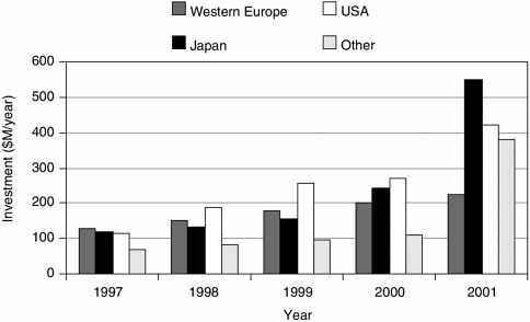
FIGURE 2-4 Worldwide government R&D spending on nanotechnology. Note that Western Europe includes the European Union and Switzerland. Countries included in the “Other” category are Australia, Canada, China, the former Soviet Union, Korea, Singapore, Taiwan, and additional countries. Finally, the entry for Japan in 2001 includes a $140 million addition to the budget that may include some programs outside the definition of nanotechnology used by the NNI. SOURCE: Data from M.C. Roco, 2001. International strategy for nanotechnology research and development. Journal of Nanoparticle Research 3(5-6): 353–360.
REFERENCES
1. International Technology Roadmap for Semiconductors. 2001. Available online at <http://public.itrs.net/> [July 1, 2002].
2. International Technology Roadmap for Semiconductors. 2001. Available online at <http://public.itrs.net/> [July 1, 2002].
3. Compaño, R. 2000. Technology Roadmap for Nanoelectronics, second edition, November. Luxembourg: Office for Official Publications of the European Communities.
4. MEMS Industry Group. 2001. 2001 Annual Report. Available online at <http://www.memsindustrygroup.org/arord01.htm> [July 2, 2002].
5. Roco, M.C., R.S. Williams, and P. Alivisatos. 2000. Nanotechnology Research Directions, IWGN Workshop Report. Boston, Mass.: Kluwer Academic Publishers.
6. National Science and Technology Council. 2000. National Technology Initiative: The Initiative and Its Implementation Plan. Available online at <http://www.nano.gov/nni2.pdf> [July 2, 2002].
7. Roco, M.C. 2001. International strategy for nanotechnology research and development. Journal of Nanoparticle Research 3(5-6): 353–360.


