
Panel III
National and International Consortia:
Lessons and Best Practices
Moderator:
Clark McFadden
Dewey & LeBoeuf LLP
COLLABORATION FOR SUCCESS IN SEMICONDUCTORS
John E. Kelly
IBM
Dr. Kelly began by referring to earlier discussions about market incentives and enhancement of manufacturing productivity. Like Dr. Freilich, he emphasized that the industry’s success will depend primarily on technical achievement. “I would argue that this industry has no future if it does not understand that it has to tackle this through technology,†he said. “It has to be driven by R&D.†He said that efficiency cannot be raised fast enough “through larger slices of glass or more efficient equipment; it has to be closed by technology. And then once that gap is closed, you cannot assume you can stand still there.†He added the second point that the United States cannot compete against companies and countries outside the United States by relying primarily on lower labor costs or larger, more productive equipment. “You fight that through innovation,†he said. “You innovate faster than anyone else.â€
Dr. Kelly said he would “draw a few analogies and some lessons learned from the semiconductor industry.†The semiconductor industry had experienced many of the same challenges as the PV industry over the past three to four decades. He listed four fundamental pressures felt by the industry on a continuing basis, “all of which have caused the industry to remake itself several timesâ€:
• Foreign competition: “We are under constant competition from low-cost entities for governments and government subsidiaries.â€
• The equipment and materials ecosystem.
• Highly skilled workforce: “As soon as you decide to compete based on innovation, you need the best work force, and that is a pipeline statement beginning with K-12 education.â€
• Research and development: Creating a leading node of logic technology now, he said, costs approximately $1 billion. “And you need to be doing three or four nodes at any given time—a big, big investment.†This ongoing expense, coupled with the slowing of semiconductor revenue increases from the high teens to the mid-single-digits, has “put industry under extreme pressure,†he said. “This has caused the industry to do things we might otherwise not have done.â€
Strength in Collaboration
The solution, Dr. Kelly said, is collaborations of many kinds between industry, government, and academia. Among examples in the semiconductor industry, he began with the Semiconductor Research Corporation (SRC), which is at the intersection of industry and academia. The second example is SEMATECH, which is at the intersection of industry and government. The third and fourth examples, he said, are new: the Nanotechnology Research Initiative and the Focus Center Research Programs. These are successful partnerships of all three sectors, he said. “Most recently, we have aligned those efforts with those of NIST and NSF, which are represented here today. We want to leverage this further into pure government-university research that is aligned with where industry needs to go. There is also extraordinary collaboration between industry players who you might think are severe competitors, but have managed to pull together to a degree which I think is probably unique in the world.â€
SEMATECH, he said, originated in the mid-1980s and gained momentum with government funding in 1988 during what was judged to be a national crisis. “We were seeing loss of share in the U.S. semiconductor industry,†observed Mr. Kelly, “but we were also seeing the entire equipment and materials base leaving the United States. That was a disaster to companies like Intel and IBM, who felt that our supply lines and the security of our own systems could be in jeopardy.†SEMATECH received $100 million from both industry and government, he said, “which I think at that time was unique.†Based on that experience, he gave his personal opinion that it would cost hundreds of millions of dollars per year to advance solar R&D and close the competitiveness gap “if we want to get off the subsidies and keep the United States in a leadership position.â€
SEMATECH itself broadened its focus from R&D to address industry standards for equipment, wafer size, packaging, “and other things we often take for granted, but which make the whole industry more efficient.†It changed further in becoming International SEMATECH, reaching out to collaborate with global members on precompetitive projects of mutual interest. In addition to increasing the number of members, it has updated its research capacity. Its original facility in
Austin, Texas, capable of producing eight-inch wafers, had been for two decades the core R&D facility, where the equipment industry, material suppliers, and small semiconductor companies went to do research. A new facility designed for 300mm wafers has now been opened in Albany, New York, for the most advanced current work.
The Value of SEMATECH to Members and Partners
Such facilities are thought to yield high value to members and partners. The average member-reported ROI is greater than five times, and the reported leverage on their yearly R&D investment is about 20 to 1. “This is what happens,†Dr. Kelly said, “when seeming competitors pool their resources. This has brought more than $2 billion in research value to members over five years.â€
The Semiconductor Research Corporation, he said, was instrumental in sustaining the essential “pipeline of skills.†“If you decide you’re going to compete on innovation, versus lowest cost only, you have to have the skills to innovate.†The SRC was formed in 1982 to help recover U.S. semiconductor market share lost to Japan. Begun as a consortium of companies to support relevant university-based research in semiconductors, it is now the largest and most successful organization of its type. In 1982, fewer than 100 students and faculty conducted silicon research. Today, the SRC has built an academic force of 500 faculty and 1,500 students. This academic community is credited with some 20 percent of the world’s research on silicon. The number of publications credited to SRC universities grew from 180 in 1981 to 2,226 in 2008. This research output, he said, is larger in some dimensions than that of some of the largest corporations in the industry. “We have put thousands of highly qualified students into the industry,†he said, “most of them hired by the member companies.â€
The SRC has also become international, collaborating on research with foreign companies. It has a focused research initiative in nanotechnology, an educational component, and Topical Research Collaborations, in which topics are chosen by participants. Such initiatives, he said, are also suitable for solar projects.
The new Focus Center Research Program (FCRP) supports collaborations between government, industry, and universities. This program was created in response to roadblocks indicated by the roadmap five to 10 years away. The five FCRP centers were established at 41 universities in 19 states to address these roadblocks “before we hit the wall.†They are funded jointly by about $20 million from both the Semiconductor Industry Association (SIA) and DARPA, which “makes a big difference in the economics of the universities.†The five centers are divided by topics in design, materials, and interconnect wiring, “and it really does represent the who’s who in the best universities in the United States. My comment here, said Dr. Kelly, is that if you want to do collaborative work between industry, universities, and government, there is a model here, with mechanisms that cover issues all the way through intellectual property, which is non-trivial.â€
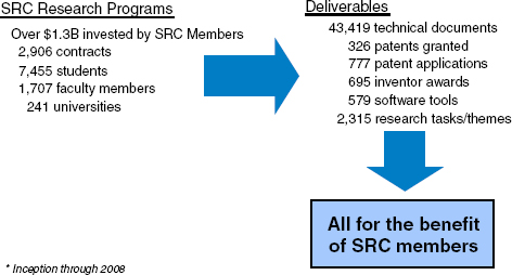
FIGURE 1 SRC numbers.
SOURCE: John Kelly, Presentation at April 23, 2009, National Academies Symposium on “The Future of Photovoltaics Manufacturing in the United States.â€
A Nanoelectronics Initiative
The Nanoelectronics Research Initiative takes an even longer view of research—beyond 10 years, when the shrinking of transistor size is projected to reach its end. “We have a few more turns of the crank left with the wonderful transistor that was invented at Bell Labs back in 1957,†Dr. Kelly said, “but beyond that we’re going to need a new switch—something far beyond the transistor as we know it today. This effort looks beyond the current silicon switch into alternate structures, such as nanotubes and quantum devices, so that new technologies are developed when we need them.†Here, too, companies have reached out to form collaborations with universities to establish large industry-funded centers with some government collaboration and considerable state funding. Four centers are set in different regions of the country, addressing five primary research vectors:
• New devices (device with alternative state vector).
• New ways to connect devices (noncharge data transfer).
• New methods for computation (nonequilibrium systems).
• New methods to manage heat (nanoscale phonon engineering).
• New methods of fabrication (directed self-assembly devices).
Dr. Kelly closed by describing an industry-only collaboration, a result of the enormous ongoing rise in research costs. IBM, he said, realized that even a company of its size could afford only three or four research nodes, so they decided a decade ago to change their model by bringing in two industrial partners. That
number has grown to eight, representing countries around the world, all collaborating in IBM labs and sharing the research risks. This “IBM Semiconductor Ecosystem†has now expanded to include other levels of collaboration, including manufacturing, design tools, design services, design IP, and more recently even the equipment suppliers. “So even within industry,†he said, “you can form these very radical collaborative efforts to tackle very large multibillion-dollar investment problems. And I think there are many lessons here that [the solar] industry needs to draw upon and move very quickly.â€
Johan Van Helleputte
IMEC
Mr. Johan Van Helleputte began with a brief review of the creation of IMEC in 1984. Recognizing that the investments required for a microelectronics research laboratory surpassed the ability of any single university, IMEC’s founder, the late Prof. Roger van Overstraeten, persuaded the government of Flanders to create and support IMEC as an independent R&D center for microelectronics. Recognizing also the need for IMEC to be effective and sustainable, Prof. Overstraeten stressed the importance of operating at a global level in order to reach a critical mass and, importantly, to work out a new business model that would maintain popular support by not using taxpayers’ money to fund research contracts with foreign firms.
This “taxpayers paradox†was resolved by organizing research around more generic problems of interest to Belgian as well as foreign companies within a larger research program, ensuring a return to the Flanders economy. This business model has proven successful. Macroeconomic impact studies have demonstrated that, IMEC’s revenues have always exceeded the government’s investment. In 2008, the government invested 44 million Euros in structural funding, while revenues were 270 million Euros. In addition, about 76 percent contract revenue for research in IMEC’s facilities in Flanders came from international companies through international collaborations, and 13 percent came from local companies, which he termed “amazingly high for such a small region†taking into account the size of IMEC.
IMEC began with a staff of about 70 people and a founding budget of 62 million Euros. By 2008, IMEC had a staff of 1,750 (about 1,650 in Leuven and 100 in Eindhoven) of whom about 1,000 are Belgians and a budget of 280 million Euros (including 45 million Euros from the Government of Flanders and 10 million Euros from the Dutch Government). Mr. Van Helleputte showed a graph depicting the evolution of staff at IMEC, whose members represent more than 60 nationalities. The international nature of the effort at IMEC is reflected both in IMEC’s payroll staff as well as in a substantial and fast-growing cadre
of employees of international companies residing at IMEC and research fellows and 185 doctoral students conducting research at IMEC. These international staff members join mixed teams with IMEC researchers, enriching the intellectual environment and technical perspectives.
A Larger R&D Reach Through Partnerships
Referring to the high complexity and cost of microelectronics research, Mr. Van Helleputte noted that “No single company could tackle all the challenges on its own.†The answer for firms lies in collaborating in R&D. Each company has a choice on how to spend the percentage of revenues it devotes to R&D: they could spend all of it on exclusive work, or they could spend part of it on a research platform, like SEMATECH or IMEC, and gain a much larger R&D reach. They could further multiply the benefits by doing it in a number of places, each time expanding their R&D reach. A central challenge for IMEC, as for similar research institutions, remains one of dealing with the combination of the huge cost of research and the rapid rate of technological change.
At the heart of research activities on the IMEC campus are two large clean rooms, one with a 200mm pilot line and one with a 300mm pilot line. Both lines are in continuous operation to maximize the return on investment in expensive equipment. The IMEC approach is to address generic problems somewhat early in a technology’s life cycle. IMEC tries to create a program based upon a forward-looking vision and by defining which research they intend to do for the next three years and then sign bilateral contracts with different companies, joining a same research program: partner A, partner B, partner C, and so on. They ask each partner to send one or more industrial residents to do joint research within the program team. The rule for intellectual property protection (IP) is that any foreground information to which the partner resident has contributed is co-owned with IMEC. If the industrial partner does not contribute to certain elements of the program, it receives a nonexclusive, nontransferable license on foreground results for its own use. This approach ensures that there are no “blind spots†in using the technology back home. At the same time, IMEC provides a nonexclusive license for the background information required to exploit the foreground results. In return for these benefits, IMEC charges an entrance fee and a yearly affiliation fee.
IMEC tries to achieve an IP policy that has something for everyone through the IMEC Industry Affiliation Program (IIAP). This program offers such variations as co-owned (shared) IP with individual companies, exclusive IP and shared (licensed) IP. “What is very important for us and for each company,†Mr. Van Helleputte said, “is not to have exclusive ownership of each subset of IP, but to have a unique IP ‘fingerprint.’ This is a combination of exclusive IP and shared IP, and these elements vary with each bilateral partnership. So, the total portfolio for each partner is unique, while at the same time the partner shares with IMEC the costs, early insight, access to IMEC results, better time to market, talent, and risks.â€
Building Technology Platforms
“An important organizational point,†Mr. Van Helleputte said, “is that IMEC begins to form its IP from a ‘research infrastructure’ on which they build ‘technology platforms’ of expertise and competence.†Building from this idea, IMEC provides a complex, five-level “leveraging strategic approach†to increase value for the institute and its partners. As stated in its overarching theme, “an R&D institute’s growth path depends on its capability to maximize its leveraging effects at different levels.†In other words, a research institute with multiple technology programs can offer them to multiple partners and harvest greater value from the resulting partnerships. “So, you’re building leverage on leverage on leverage,†said Mr. Van Helleputte “and you reuse the mechanism of co-ownership without any accounting to each other about the foreground research.â€
He turned to IMEC’s strategic orientation in view of industry trends. He said that industry is now making a distinction between “More Mooreâ€â€”continued CMOS scaling and maximization of chip performance—and “More than Moore†or maximizing the functionality of single chips. The first approach focuses predominantly on device performance where materials are paramount, with lithography being an instrumental path of research. The second approach focuses on heterogeneous integration of different functionalities into a single chip (SOC) or into a single package (System-in-a-package). In More Moore, IMEC is now working on 22nm, 16nm, and even smaller devices, where new materials and device research are central. “IMEC tries to explore multiple options,†he said, “so companies can see at an early stage which one has a chance to become a market winner.†He added that with a “core partner system,†each core partner can subscribe to a total menu of programs or choose a subset of those. These partners include “the whole ecosystem†of firms: leading integrated device manufacturers, memory suppliers, logic suppliers, equipment and material suppliers, pure foundries and designers.
Help with Custom Applications
Mr. Van Helleputte described a new initiative called CMORE that builds on the existing infrastructure and technology platforms to aim at custom application solutions.15 “For example,†he said, IMEC can work with companies that may have a brilliant new idea but have difficulty implementing it in a commercial setting. This involves first testing the technical feasibility,†which “may involve joint R&D, development-on-demand, prototyping, and low-volume production.†He mentioned the case of a partner who asked for help putting 10 million mirrors on a chip that could be steered individually. The chip had to be
____________________
15IMEC’s CMORE initiative is a platform designed to allow companies to turn their innovative concepts into packaged microsystems products, based on IMEC’s expertise in the field.
no larger than 10 square centimeters and achieve 1012 cycles without fatigue or creep. “That,†he said,†was a typical example of Development-on-Demand CMORE activity.â€
IMEC has several major application programs under the “More than Moore†umbrella that build on its expertise in semiconductors. These include
• Communications technologies: Cognitive reconfigurable radio and >60GHz communication, and ULP-Radio;
• Biomedical electronics: wearable health and comfort monitoring; brain-IC interfaces/neuro-electronics; smart implants and biosensor technology based on nanotechnologies;
• A new Center for Neuro-Electronics Research/Flanders (NERF), part of a new interdisciplinary research center for the integration of neuroscience and neuro-electronics & clinical experimental neurosurgery. NERF is hosted at IMEC; and
• Energy: PV, GaN/Si for power switching and solid-state lighting.
IMEC’s Solar Research
“Indeed, IMEC has a substantial PV program as well, and the workhorse of the program is silicon PV for the reason that we have a lot of expertise in silicon and that there is still a lot of room for improvement,†noted Mr. Van Helleputte. “And we do believe that there is room for both thin-film and crystalline silicon in the future. Companies like First Solar, will push toward a further acceleration of the PV roadmap and IMEC will gladly respond to such a challenge.†IMEC also has an activity with organic PV and with highly efficient PV stacks for solar concentration. The IMEC program on crystalline silicon PV research has a number of research modules, with two major themes: One is a wafer-based approach, and the second explores epitaxial thin film on silicon. They are experimenting as well with new ways to produce ultrathin wafers without the kerf losses incurred in cutting ingots. These are called stress-induced lift-off methods (SLIM) where the active wafer is lifted off a substrate rather than cut.
Finally, IMEC is experimenting with a stacked approach for concentrator solar cells (CPV) as an alternative to monolithic approaches. In this design, each layered cell absorbs a part of the light spectrum, not all of it, combining its contribution with those of the other cells. “It is more complex,†he said, “but it avoids some technical drawbacks of the monolithic approach (such as tunnel junctions and current matching), and may increase conversion efficiency and energy yield, although this has not yet been proved in a total system approach.â€
Mr. Van Helleputte concluded by mentioning the Solar Europe Industrial Initiative, which has included on its roadmap the goal of meeting 12 percent of electricity demand from PV sources by 2020. “To accomplish this,†he said, “Europe would have to develop about 350 gigawatts of PV capacity.†“And it also
assumes that by 2020 the lifetime of the solar modules will be 30 years,†he said, “this is quite ambitious.â€
PUBLIC-PRIVATE R&D COLLABORATION: LESSONS FROM PV PARTNERSHIPS
Robert M. Margolis
National Renewable Energy Laboratory
Dr. Margolis said he would speak about trends in PV development, the DoE’s Solar program, and lessons from several public-private partnerships. He began with some background on the global PV industry and investment trends highlighting the fact that global PV production has been growing very rapidly over the past couple of decades and that both public and private sector investment in PV technology has grown dramatically during the past four to five years. In 1980, the United States was responsible for more than 75 percent of global PV production in what was then a nascent market. By the 1990s, Japan had begun a federal program of incentives and quickly became the global market leader; the U.S. share of production dropped to the 30 percent to 50 percent range. In the past decade, leadership has shifted to European countries and, more recently, China and Taiwan have expanded production rapidly. Cumulative installed photovoltaic (PV) capacity worldwide as of the end of 2008 was estimated to be 13.7 GW. Germany was the leader at 5.4 GW of cumulative installed capacity, followed by Spain, Japan, the United States, South Korea, Italy, and France. U.S. cumulative installed PV capacity through 2008 was 1.1 GW. California continued to dominate the market with 530 MW in cumulative installed capacity, a 67 percent market share, with New Jersey second at 70 MW or 9 percent market share. U.S. cumulative installed capacity of 1.1 GW was a 43 percent increase over 0.77 GW in 2007.16 While the growth in PV production and installations has been very rapid, PV still accounts for only a small fraction of U.S. generating capacity.
In addition to rapid growth in production, the growth in investments in solar technologies has been dramatic during the past couple of years. Just five or six years ago, according to data from New Energy Finance, only a few tens of millions of dollars were going into PV from the private sector; this figure had risen to tens of billions of dollars a year. “This has been a dramatic change,†said Dr. Margolis, “and has had a very big impact on how the industry is organized, how it does R&D, and how it interacts with the government.â€
Venture capital and private equity, he said, have taken on a larger role beginning in the mid-2000s, and especially in the last three years. This investment varies enormously by region and technology. For example, the EU has invested primarily in crystalline silicon technologies and project development. In contrast,
____________________
16Data drawn from numerous sources as presented in Price and Margolis (2009).
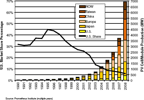
FIGURE 2 Historical global PV production and U.S. market share.
SOURCE: Robert Margolis, Presentation at April 23, 2009, National Academies Symposium on “The Future of Photovoltaics Manufacturing in the United States.â€
U.S. investors have been pursuing a much more diverse set of technologies than investors in other regions. Significant investments in the United States are going into thin-film technologies, multijunction concentrating PV technologies, and next-generation PV technologies. Of about 200 companies that received private-sector investment in the past three years, more than 100 are in the United States Asia has focused primarily on existing crystalline silicon technologies, with a small shift toward thin-film technologies during 2008. Asia also has been making significant investments in polysilicion production.
A Five-Year Projection
Dr. Margolis presented a meta-analysis of near-term projections from about a dozen analysts. According to this set of projections, a five-fold increase in PV production is expected to occur between 2008 and 2012. Crystalline silicon is expected to remain dominant, with thin-film technologies growing more rapidly than they have in the past. “But we’ve also learned that things can change really fast,†he said. “For example, the global economic crisis may bring about lots of changes going forward, and already many analysts have lowered their projected 10-25 percent.â€
Global PV industry revenues are also projected to continue rising. The current level of revenues across the PV supply chain was about $30 billion in 2008. He said this level of revenues places the PV industry where the semiconductor industry was in the early 1980s. “So maybe this is the perfect time to discuss whether SEMATECH is the right model. The industry is getting to a similar scale of production to where the semiconductor industry was in the early 1980s, and going forward we’re talking about billions of dollars of investment in new PV ‘fab’ facilities.â€
Next, Dr. Margolis turned to the Department of Energy’s Solar Program, which received steady funding of about $80 million from FY2001 to FY2006. Then, in FY2007, the Solar Program’s budget increased substantially, under the Solar America Initiative, to about $160 million per year. This is expected to increase again under the new Obama administration, with new resources to leverage private sector investments through a host of collaborative mechanisms.
The DoE solar R&D pipeline, he went on, is not really a linear process, but one with feedbacks and interactions. He focused on one piece, the Technology Pathway Partnerships (TPPs). The whole pipeline supports many early-stage partnerships between universities and other parts of the supply chain. The TPPs started in 1997 with a three-year grant of $168 million in DoE funds, and a total of $357 million including industry matching funds. This represented a shift from the prior focus on the device and module level to an emphasis on total system costs, including installation, inverters, and balance of system components. The partnerships, some of them with over a dozen members, included more than 50 companies, 14 universities, three nonprofits, and two national labs. Dr. Margolis suggested that this experiment might be a model for how to foster collaboration across different actors in the PV industry.
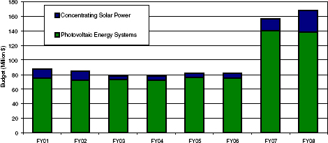
FIGURE 3 DoE solar program funding FY2001-FY2008.
SOURCE: Robert Margolis, Presentation at April 23, 2009, National Academies Symposium on “The Future of Photovoltaics Manufacturing in the United States.â€
A precursor to the TPPs was the PV Manufacturing/PV Manufacturing R&D (PVMaT/PVMR&D) project that was started in 1991. Its original goal was “… to ensure that U.S. industry retain and extend its world leadership role in the manufacture and commercial development of PV components and systems.â€17 This was the period when the U.S. market share was declining from 75 percent to 30-50 percent. The PVMaT/PVMR&D Project was a collaborative effort focused on helping the PV industry improve its manufacturing processes and equipment, accelerate cost reductions, raise commercial product performance and reliability, and lay the groundwork for scale-up of U.S.-based PV manufacturing capacity. The project was carried out over a 15-year period and was funded with about $150 million in federal money matched by a roughly equal amount of private-sector money. The project was considered innovative in its use of multiyear contracting and cost sharing. About three-quarters of the completed projects achieved cost reductions, increased output, and improved efficiencies. For 14 manufacturing R&D participants, the cost of manufacturing came down 54 percent and manufacturing capacity increased by a factor of 17.
Tools for Partnerships
Dr. Margolis reviewed the tools used for the partnerships funded through the PVMaT/PVMR&D, beginning with cost sharing. The approach to cost sharing ensures both the sharing of R&D risk and enabled firms to own any resulting IP. Also built into the proposal was an evaluation process, as well as key collaborative aspects, beginning with problem identification. In 1991, 22 firms were selected through a competitive bidding process. They each received $50,000 for phase 1, a three-month study, which was required to qualify for phase 2. This stimulated the involvement of many people, he said, and was effective in educating DoE and NREL on critical manufacturing problems. The evaluation process was carried out by independent panels of representatives from industry, government, and universities who helped establish the credibility of the project. It was a challenge for government to give up some control, find good people for the panels, and keep panels together. One constructive response was to hold annual review meetings, which provided a venue for participants to interact and share results.
An approach that did not succeed was a plan to form teams for generic research on problems of common interest to companies. A key roadblock was concern over IP. This is still an issue in precompetitive research, he said, though it is better understood.
Dr. Margolis closed with several conclusions. First, the PVMaT/PVMR&D
____________________
17C. E. Witt, R. L. Mitchell, and G. D. Mooney, “Overview of the Photovoltaic Manufacturing Technology (PVMaT) Project.†Paper presented at the 1993 National Heath Transfer Conference, August 8-11, 1993, Atlanta, Georgia, August 1993.
project used innovative forms of cost sharing and collaboration to strengthen information flows between partners. Second, under the TPPs, DoE encourages vertical collaboration—across the value chain—which has helped move the industry from a component focus to a systems-level focus. And finally, the DoE’s approach to engaging the private sector in collaborative R&D will need to evolve as the PV industry grows and matures.
DISCUSSION
A questioner asked about forming industry consortia in such a diverse industry. With so many technologies, he asked, what kind of critical mass do you need? Won’t some players decide to go it alone? Dr. Margolis answered that on the basis of the semiconductor experience, the majority of the large players must participate, and there must be some mechanism for the involvement of the industry as a whole. In the case of the SIA, he said, consortia needed the top dozen or so semiconductor CEOs, as well as mechanisms to bring in other participants. For the PV industry, it would include the module manufacturers and significant suppliers of that value chain. He added that the government can help bring the right people together. Eventually, in the case of the semiconductor industry, “people were suddenly afraid of being left out rather than concerned about how to jump in. Even fierce, fierce competitors came to the table and worked together.â€


