
4
Emerging Technologies with Potentially Significant Impacts
INTRODUCTION
The ultimate performance of a particular detector system is dependent on the integration of the various component technologies. Chapter 3 discusses the current and anticipated 10-15 year status of the various detector component technologies together with their likely impact on overall system performance. In contrast, this chapter focuses on technology breakthroughs that are more speculative in nature but, if achieved, could represent “game changing” improvements in system-level detector performance. Technologies enabling (1) advanced detection, (2) innovative optics, (3) improved coolers, and (4) enhanced signal processing are discussed in detail.
ADVANCED DETECTION TECHNOLOGIES
Epitaxial Growth Approaches
Epitaxial growth techniques are used to produce the active material in most long-wavelength infrared (LWIR) photon detectors. The detector material generally consists of two or more thin layers grown in succession on a substrate. Epitaxial growth implies that the crystal structure of the layers is aligned with that of the substrate, a necessary requirement for good material quality and appropriate electrical characteristics. The two most common families of epitaxial materials for LWIR applications are mercury cadmium telluride (MCT) and antimonide-based III-Vs.
For MCT, the technique of liquid-phase epitaxy (LPE) was demonstrated in the early 1980s and has matured to become a workhorse of the industry. Elements to form the layers are first dissolved in a melt of mercury or tellurium. The substrate is immersed in the melt and the temperature is ramped down, causing the elements to crystallize and form a layer. A second melt is used to form a second layer. N-type and p-type dopants, respectively, are included in the melts, so that the interface between layers becomes a p-n junction. The substrate for nearly all LPE growth is cadmium zinc telluride (CZT), which is chemically and physically compatible with MCT and is transparent in the IR.
Advantages of LPE are that (1) it occurs close to thermodynamic equilibrium, typically near 500°C, causing it to be relatively forgiving of defects; (2) dopants can be incorporated in a very controllable manner; and (3) excellent material quality is routinely achieved. The disadvantages are that detector structures requiring more than two layers are impractical, and it is not possible to maintain sharp interfaces between layers because of interdiffusion during growth. Also, LPE growth cannot be performed on alternative substrates such as silicon.
Molecular beam epitaxy (MBE) has become the preferred growth method for more advanced MCT device structures, such as two-color arrays for third-generation sensors, as well as avalanche photodiodes. It also enables the growth of MCT on silicon and GaAs substrates that are larger and cheaper than CZT. MBE growth is performed in an ultrahigh-vacuum chamber with the elements being emitted by hot effusion cells and depositing on the substrate, which is held at about 200°C. Sharp interfaces can be formed because the molecular beams can be turned on and off abruptly and because interdiffusion is negligible at the low growth temperature. In most cases the substrate is CZT, silicon, or GaAs.
MBE is more challenging than LPE because it is less tolerant of growth defects, and it requires very tight control of the substrate temperature and the beam pressures of the species arriving at the substrate. MBE equipment is more expensive to acquire and maintain than that of LPE. However, MBE technology has matured to the point that multilayer epitaxial structures, in which the MCT alloy composition and the doping are controllably changed several times during the growth run, are produced on a regular basis. This has enabled complex device structures in MCT that would have otherwise not been possible. Also, the ability to grow MCT on silicon has enabled the fabrication of very large focal plane arrays (FPAs). There is a large lattice mismatch between HgCdTe and both GaAs and silicon, which has severe implications for the growth process, in particular the formation of dislocations and other growth defects. Significant progress has been made in learning how to accommodate the lattice mismatch, particularly in the HgCdTe:GaAs system as discussed in Chapter 3. The availability of larger and cheaper substrates for epitaxial growth will have a major impact on the performance and cost of future HgCdTe FPAs.
The antimonide-based III-V materials, including strain-layer superlattice (SLS), quantum-well infrared photodetector (QWIP), and quantum-dot infrared photodetector (QDIP) structures, are grown by MBE in most cases. The technique is similar to that for MCT, except that the substrate temperature is higher (about 400 to 500°C). MBE technology for III-V materials is relatively mature, but some additional development has been required to control the composition of the atomic monolayers at the interfaces between the indium arsenide and the gallium antimonide components of the SLS in order to control the strain. Further improvements in the MBE technique are needed to minimize the populations of point defects that limit the carrier lifetimes in SLS material. The large experience base in the growth and design of electronic and photonic devices using bandgap engineering—the incorporation of multiple functional layers into device structures—opens new avenues for optimizing device performance. Examples include barrier layers to reduce dark current and amplification layers to extend the concepts of avalanche gain and Geiger mode detection further into the IR. Most of these efforts are at an early stage of research development and are likely to bear significant fruit within the next 15 years. This is an area to pay attention to for further improvements in infrared detection.
Nanophotonics
Over the recent past, the global scientific community gradually developed technologies that could structure materials on a nanometer scale and the field of nanotechnology was developed. Arguably, nanotechnology has its roots in the challenge of Professor Richard Feynman in 1959 to build the world’s smallest motor.1 In 1996, a federal interagency working group was formed to consider the creation of a National Nanotechnology Initiative (NNI) to focus U.S. research and development (R&D) efforts,2 and in 2000 the NNI became a formal government program. In 2003, the 21st Century Nanotechnology Research and Development Act (NRDA) gave the NNI the legislative backing needed to establish a management structure and funding.3 The National Science Foundation has played a key role, leading and coordinating the various agencies involved, including the Department of Defense, the Department of Energy, the Environmental Protection Agency, the National Institutes of Heath, the Department of Commerce, the U.S. Department of Agriculture, the National Aeronautics and Space Administration, and many
others. In the past several years, the annual funding for the NNI has been at about $1.5 billion.4 Table 4-1 shows the distribution among the various funding sources within the U.S. government.
A similar historical evolution has occurred in many foreign countries.5 The intent in this chapter is not to provide exhaustive historical detail; in short, Japan, Europe, and other Asian countries have kept pace with the United States with comparable government expenditures and even more significant commercial funding. Much of the work up to the past half dozen years has been oriented toward fundamental materials, establishing methods for creating nanometer structures and measuring properties. More recently, efforts have matured for building entirely new device structures using these material fabrication techniques. Quantum dots, nanotubes, and layered carbon graphene structures can be cited as examples of specific materials from which entirely new devices and applications will arise. Countries around the world are poised to take advantage of nanotechnology to potentially build entirely new sensors and sensor systems. Therefore, foreign progress in the nanotechnology field constitutes a principal driver for significant advances in sensors.
Of the many nanoscale material systems being explored, simple carbon structures are undoubtedly the most studied; perhaps these carbon structures will be, in fact, the “silicon” for nanotechnology. With several different morphologies (graphene two-dimensional [2-D] or three-dimensional [3-D] layered structures, spherical fullerene [“Bucky Balls”], and single- and multiwall nanotubes [CNT] of different chiralities) and outstanding physical properties (>30× the strength of steel and approaching the conductivity of copper), carbon is being studied for a host of applications. All of the III-V and II-VI compound classes are also extensively being explored for basic science attributes and applications; hence, techniques have emerged for reproducible quality device prototypes using the full power of modern electronic material and chip fabrication methods. It would distract us in this short introduction to list the many other types of materials such as biology-based building blocks that might have some bearing on new techniques for sensors; instead it suits our purpose here to focus on the most significant potential that nanomaterials can provide to advance the sensor state of the art. The impact of nanotechnology on future designs of sensors and sensor systems can be anticipated along the following lines.
Graphene is a material that has recently been a subject of intense study for its potential application in high-frequency electronics and photonics. Graphene consists of a monolayer of carbon atoms arranged in a 2-D hexagonal lattice.
|
4 |
Available at www.nano.gov/NNI_FY09_budget_summary.pdf. Accessed March 25, 2010. |
|
5 |
Woodhouse, E.J., ed. 2004. Special Issue on Nanotechnology. Prepared as a Publication of the IEEE Society on Social Implications of Technology. IEEE Technology and Society Magazine 23(4). |
TABLE 4-1 Funding of Nanophotonics by Federal Agency
|
|
2009 Actual |
2009 Recoverya |
2010 Estimated |
2010 Proposed |
|
DOEb |
332.6 |
293.2 |
372.9 |
423.9 |
|
NSF |
408.6 |
101.2 |
417.7 |
401.3 |
|
HHS-NIH |
342.8 |
73.4 |
360.6 |
382.4 |
|
DODc |
459.0 |
0.0 |
436.4 |
348.5 |
|
DOC-NIST |
93.4 |
43.4 |
114.4 |
108.0 |
|
EPA |
11.6 |
0.0 |
17.7 |
20.0 |
|
HHS-NIOSH |
6.7 |
0.0 |
9.5 |
16.5 |
|
NASA |
13.7 |
0.0 |
13.7 |
15.8 |
|
HHS-FDA |
6.5 |
0.0 |
7.3 |
15.0 |
|
DHS |
9.1 |
0.0 |
11.7 |
11.7 |
|
USDA-NIFA |
9.9 |
0.0 |
10.4 |
8.9 |
|
USDA-FS |
5.4 |
0.0 |
5.4 |
5.4 |
|
CPSC |
0.2 |
0.0 |
0.2 |
2.2 |
|
DOT-FHWA |
0.9 |
0.0 |
3.2 |
2.0 |
|
DOJ |
1.2 |
0.0 |
0.0 |
0.0 |
|
TOTALd |
1,701.5 |
511.3 |
1,781.1 |
1,761.6 |
|
NOTE: CPSC = Consumer Product Safety Commission; DHS = Department of Homeland Security; DOC = Deparment of Commerce; DOD = Department of Defense; DOE = Department of Energy; DOJ = Department of Justice; DOT = Department of Transportation; EPA = Environmental Protection Agency; FDA = Food and Drug Administration; FHWA = Federal Highway Administration; HHS = Department of Health and Human Services; NASA = National Aeronautics and Space Administraion; NIFA = National Institute of Food and Agriculture; NIH = National Institutes of Health; NIOSH = National Institute for Occupational Safety and Health; NIST = National Institute of Standards and Technology; NSF = National Science Foundation; USDA = Department of Agriculture. aBased on allocations of the American Recovery and Reinvestment Act (ARRA) of 2009 (P.L. 111-5) appropriations. Agencies may report additional ARRA funding for small business innovative research (SBIR) and small business technology transfer (STTR) projects later, when 2009 SBIR-STTR data become available. bIncludes the Office of Science, the Office of Energy Efficiency and Renewable Energy, the Office of Fossil Energy, the Office of Nuclear Energy, and the Advanced Research Projects Agency-Energy. cThe 2009 and 2010 DOD figures include congressionally directed funding that is outside the NNI plan ($117 million for 2009). dTotals may not add, due to rounding. SOURCE: Data from http://www.nano.gov/html/about/funding.html. Accessed May 2, 2010. |
||||
Electronically, it behaves as a zero bandgap semiconductor with extraordinary carrier mobility, even at room temperature. Graphene has also demonstrated strong photocurrent responses near graphene-metal interfaces. The combination of graphene’s attractive electronic and photonic properties holds great promise for visible detector applications. In fact, recent results have demonstrated the use of graphene detectors in a 10 gigabit per second optical link with an external photoresponsivity of 6.1 mA/W at 1.55 μm wavelength.6 The same group also reports
having demonstrated a strong photoresponse in a metal-graphene-metal (MGM) based photodetector at 514 nm, 633 nm, and 2.4 μm. Graphene’s high switching speed combined with a broadband photoresponse underscores its potential to have a disruptive impact on future detector performance. The promise of a material that may surpass the performance of silicon for many electronic applications has focused a significant body of research on graphene because the mechanisms of transport in this material are not fully understood. As these research efforts mature over the next several years and new techniques for processing and fabricating graphene devices are developed, the true potential for graphene in electronic and photonic devices will become better clarified and quantified.
Photonic Structures
Nanostructures can be built through bottom-up self-assembly processes taking advantage of both organic and inorganic routes and top-down approaches applying lithographic techniques. Integrated circuit scales are approaching transverse dimensions of ~10 nm scale,7 and an important trend is the merging of top-down processes, which offer long-range order and complex hierarchical structure, and bottom-up self-assembly, which offers nanometer-scale capabilities and below, with “directed self-assembly.”8 Since the first demonstration9 of a photonic crystal in 1989, detailed work has accelerated quickly and been extended from microwave to optical frequencies. Again, not to dwell on explanations that can be found in textbooks,10 the concepts use the precision attendant to nanostructure construction to form periodic one-, two-, and three-dimensional subwavelength structures for controlling optical radiation. Analogous to electrons in semiconductors, light propagates through periodic structures with pass bands or stop bands depending on the wavelength. All of the well-known components familiar to microwave engineers can therefore be constructed for light—for example, wavelength pass-rejection filters, resonators, isolators, circulators, and bends. Embedding absorbing or emitting optical elements in these structures permits tailoring of features such as spontaneous emission probability through a lower density of radiation states. In addition to potential advantages in designing more compact optical trains trans-
|
7 |
Data derived from the International Technology Roadmap for Semiconductors, available at http://www.itrs.net. Accessed March 25, 2010. |
|
8 |
J.A. Liddle, Y. Cui, and P. Alivasatos. 2004. Lithographically directed self-assembly of nanostructures. Journal of Vacuum Science and Technology B 22(6):3409-3414. |
|
9 |
E.Yablonovitch and T.J. Gmitter. 1989. Photonic band structure: the face-centered cubic case. Physics Review Letters 63:1950-1953. |
|
10 |
J.D. Joannapoulos, S.G. Johnson, J.N. Winn, and R.D. Meade. 2008. Photonic Crystals: Molding the Flow of Light. Princeton, N.J.: Princeton University Press. |
porting light from the collection aperture to the detector element, some tailoring of the thermal noise background is possible.11
These structures should not be confused with composite dielectrics, which are composed of two or more materials interspersed on a subwavelength scale without any consideration for ordering. An example is perfectly black carbon surfaces comprising “steel wool-like” features or a mixture of low- and high-index material to achieve a particular index of refraction. While subwavelength surface absorbing elements do imply the possibility of building sensors with subwavelength pixel size, diffraction effects limit the minimum pixel sizes independent of the length scale of the absorber as discussed in Chapter 2. Metamaterials are an emerging class of materials with wholly new properties such as a negative index of refraction that offer additional possibilities for managing and directing optical paths in nonclassical ways.12 Additionally, plasmonics takes advantage of the very large (and negative) dielectric constant of metals, to compress the wavelength and enhance electromagnetic fields in the vicinity of metal conductors. This has been referred to as “ultraviolet wavelengths at optical frequencies”13 and is the basis of many well-studied phenomena such as surface-enhanced Raman scattering (SERS) and surface plasma wave chemical-biological sensors.14 Additional discussion of the application to infrared detectors is presented in the following section.
Electronics
The broad applicability of nanotechnology to electronics is obvious; for example, the use of cathodic electron field emission from an assemblage of nanotubes for high-power microwave transmitters15 and other vacuum electronic applications offers copious production of electrons; this particular technology may find immediate application in fielded systems. On an individual scale, single-wall carbon nanotubes (SWNTs) can be isolated with adequate properties16 to demonstrate transistor action for microelectronic circuits. Techniques for generating and manipulating individual SWNTs have been perfected to the point that metal-metal,
metal-semiconductor, and semiconductor-semiconductor junctions can be reproducibly formed and the I-V curves measured;17 however, scaling this to the densities and defect levels already reached for complementary metal oxide semiconductor (CMOS) applications remains an open question. It can be noted that this last reference is from the Indian Institute of Science in Bangalore, illustrating the global sweep of this important technology. SWNTs have been assembled into electronic circuits in elementary “chips” with >20,000 elements,18 and field effect transistors (FETs) have been reproducibly constructed to build a 10 FET ring oscillator.19 Competitive electronic applications are many years behind the level of sophistication needed to contemplate actual integration of a nanoscale readout integrated circuit (ROIC) into operating sensors. Still the ultimate payoff of a fully integrated sensor element with nanoscale processing requires ongoing monitoring of global improvement and activity.
Sensor Elements
Quantum sensor elements receive an incoming photon and free a bound electron(s) for amplification and signal processing. The nanomaterial necessarily must have well-defined optical and electronic properties. One such material is a quantum dot wherein the physical dimensions are reduced to the point that electron states are no longer defined by an infinite crystal lattice; rather, the dot’s physical dimension fixes the permissible energy bands, very much a man-made atomic system. Quantum-well structures also tailor bands, and QWIP sensor elements are discussed in another section of this report along with pixel-sized antennas to guide incoming radiation into the element. At this stage of nanotechnology detector elements, QWIP and QDIP structures are the most studied, but entirely new configurations might be possible and literature should be appropriately scanned.
Plasmonic Enhancement of Detectors
The dielectric properties of metals are often described by a free-carrier Drüde model given by
where
is the plasma frequency in the metal, with e the electronic charge, N the carrier concentration, κ the relative dielectric constant arising from the bound electrons, and m* the electron effective mass. For single-electron per atom metals such as gold and silver, ωp is in the ultraviolet spectral region. Here ν is the electron collision frequency that is typically in the terahertz regime. At radio frequencies, ω/ν << 1, and the metal response is large and imaginary (out of phase with the driving electric field). Throughout the infrared, ω/ν >> 1, and the metal response is large and negative with a smaller imaginary part. This is the plasmonic regime. At visible frequencies, additional losses due to bound electron transitions become more important and the dielectric function is both lossier and not as negative. For most metals except gold, silver, and aluminum, the dielectric function is positive across the visible.
Some of the implications of this dielectric function have been recognized for more than 100 years. Sommerfeld was the first to recognize the existence of a bound surface mode at the interface between a lossless dielectric and a lossy metal in his analysis of Marconi’s wireless transmission experiments (there the loss was associated with currents in Earth’s surface).20,21,22 More recently, interest in plasmonics has been rekindled with the discovery of anomalous transmission through a metal slab perforated with a 2-D array of holes.23,24 This transmission is associated with resonances involving the coupling of the incident radiation to surface plasma waves (SPW) localized to a metal-dielectric interface (a thin metal film has two such SPWs one on either side of the film) and the localized resonances associated with the holes (or other unit-cell structures such as annuli25).
The implications for detectors were recognized quite some time ago26 and rediscovered soon after the discovery of the anomalous transmission.27 In addition to the distributed SPW coupling, work has also been reported using a shaped plasmonic lens structure to funnel all of the incident radiation to a single small detector at the center of a bull’s-eye pattern.28 This particular experiment was for a SWIR detector for integration with silicon integrated circuits, and the goal was reduced capacitance for higher-speed operation. For the infrared, this approach is aimed mainly at reducing the detector volume and, consequently, thermal noise sources such as generation-recombination dark current in high-operating-temperature MWIR detectors.29 The difficulty is finding the appropriate combination of SPW coupling, hole transmission, and angular and spectral bandwidth while still retaining the ability to collect the photo- or plasmon-generated carriers.
Very recently, a 30× enhancement in detectivity was obtained for a SPW coupled QDIP detector30 by coupling using a similar transmission metal grating. This is very early work, still in the exploratory research stage, and far from ready for integration into commercial focal planes, but it does offer the potential of a multispectral, MWIR-LWIR focal plane array with high quantum efficiency, polarization, and spectral selectivity and some degree of electrical tuning based on the quantum-confined Stark effect in QDIP detectors. Ultimately, based on previous results on coupling to SPWs, quantum efficiencies near unity should be possible. These arrays could be a new direction in IR FPAs; however, the road to a fielded product is long and success is not guaranteed. The difficulty is finding the appropriate combination of SPW coupling, hole transmission, and angular and spectral bandwidth while still retaining the ability to collect the photo- or plasmon-generated carriers.
FINDING 4-1
An emerging trend in focal plane array technologies is multispectral band sensing enabling enhanced system capability through a single aperture. Spectral information is an added discriminant for enhanced detection selectivity and material identification.
FINDING 4-2
By manipulating fields at the subwavelength scale, nanophotonics offers a potential for enhanced detector functionality, particularly in adding wavelength and/or polarization selectivity along with enhanced detectivity at the pixel scale.
Antennas
An antenna is a transduction device that is used to transmit or receive electromagnetic radiation. Traditionally, antennas have been associated with transmit or receive applications in the radio-frequency (RF) spectrum. Examples of RF antennas can be found in many aspects of everyday life since they are a ubiquitous component in television, radio, voice, data, radar, and other communication networks. However, within the past decade, the potential for developing antennas that work in the visible and IR spectra has been explored with increasing interest. In this section, recent research in IR and optical antennas is reviewed and assessed in terms of relevance to visible and IR detector technologies.
Antennas are composed of various conducting elements arranged in a pattern designed for optimum performance for a given application. Typical performance parameters cited are gain, bandwidth, and efficiency and these are all functionally related to both the size of the antenna elements and the conducting (electrical and magnetic) properties of the materials that comprise the antenna. While the basic equations that govern antenna performance in the RF spectrum have analogues in the IR and optical spectra, the physical realization of elements that constitute a functional antenna are vastly different. The two major reasons for these differences include the fact that antenna size scales with wavelength and that material losses increase significantly in conductors with increased frequency. The scaling issue requires that antennas working in the IR and optical spectra be typically on the order of microns or smaller, and the loss issue presents significant challenges in designing antennas that achieve reasonable efficiencies at IR and/or optical wavelengths.
Despite the challenges in developing antennas for optical and/or IR applications, there has been a significant body of research focused on exploring this topic. The primary drivers for this research are the need for achieving large absorption cross section together with high field localization and/or enhancement for applications in nanoscale imaging and spectroscopy, solar energy conversion, and coherent control of light emission and/or absorption.31 It is difficult to speculate on the
potential future impact of optical-IR antennas on detector systems at this time due to the fundamental and immature status of the research. It is worth considering, however, how an optical and/or IR antenna might be employed in a detector system and what performance benefits it might enable.
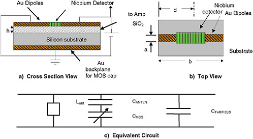
One example is to exploit the wavelength and polarization selectivity of antennas to enable detectors with electronically tunable spectral responses. A brief discussion of this concept follows. An antenna-coupled IR sensor receives flux with an antenna that is tuned to optical wavelengths, and only photons in a selective waveband pass into the detector. Typically the antenna is used to receive radiation and is coupled to an infrared or thermal detector to capture the signal power. Such devices have been used for infrared and millimeter-wave sensing. One advantage of an antenna-coupled IR sensor is that spectral and polarization responsivities can be set by antenna size and orientation. In addition, the spectral response of these devices can be tuned electronically.32 Typical devices are fabricated on top of a dielectrically coated metallic ground plane as shown in Figure 4-1(a) and 4-1(b), in cross section and top views, respectively. Figure 4-1(c) shows an equivalent circuit model that was developed for a device that incorporated a metal oxide semiconductor (MOS) capacitor for spectral tuning. The gold antenna arms, the SiO2, and the silicon substrate form the MOS-cap. Applying bias to the backside of the silicon changes the depletion width of the capacitor.
The MOS-capacitor pair acts as a varactor (Cmos), in series with the antenna capacitance Cantenna. Their equivalent capacitance Ceq, is in parallel with the antenna inductance Lantenna and the fringe-field capacitance Cfarfield. When the MOS-capacitor is biased in the depletion region, Weff continues to expand until the device enters into the inversion region. Figure 4-2 displays both the measured and modeled results from an IR MOS tuner.33 It shows actual tuning of a nanofabricated antenna, coupled with a conventional photodetector. These measured results were taken with a single antenna that was hand-fabricated by etching with a mask made by simple contact photolithographic masking. Higher precision would be expected in production, with the use of more sophisticated fabrication and measurement
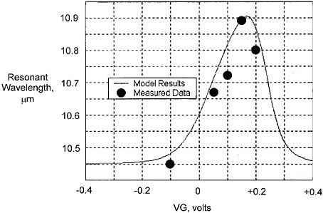
equipment. Nonetheless, the tunability of this antenna structure is evident, as is the accuracy of the predictive model, showing practicality of design and fabrication.
FINDING 4-3
IR and/or optical antennas for detectors are theoretically capable of surpassing current uncooled bolometer detector sensitivity, specifically in the MWIR. However without significant investments in materials, manufacturing, and fabrication, systems based on antenna technology are not likely to achieve a maturity level that would enable their practical use in a 10-15 year time frame.
Wavelength Up-conversion
In principle, wavelength conversion is very attractive. Visible detectors are inexpensive, sensitive, and uncooled; have huge formats; and have very small pixel pitch. Visible detectors are superior to all subbands of infrared detectors in almost all aspects. The concept of wavelength conversion from an infrared wavelength to the visible would make these inexpensive, superior, focal planes available to detect radiation at infrared wavelengths. Unfortunately up-conversion has not achieved significant success to date. Visible photons contain more energy than infrared photons. Energy must be added to convert IR photons to visible photons. A pump will be required that adds energy, preferably without adding significant noise. An alternate way to approach up-conversion could be to have IR photons driving the emission of visible photons.34 Major issues for any up-conversion approach are (1) achieving high conversion efficiency and (2) minimizing noise added by the up-conversion process. Background-limited infrared photodetection (BLIP) performance, or near-BLIP, performance is desired.
A variety of physical mechanisms have been attempted for up-conversion without achieving practical device-level success. Some recent schemes have focused on variants to achieving room-temperature detectors as an alternative to microbolometers: (1) free carriers in silicon using reemission from silicon clusters,35 and (2) optical refractive index change with absorbed radiation.36 These sensor concepts may find use in specialized applications but have yet to provide a competitive level of performance. In this class of technologies, a film or material of some sort is used with a bandgap that is too large to absorb infrared radiation. A pump laser, or potentially some other energy source, is used to keep the material in a metastable
|
34 |
Hui Chun Liu. 2006. Photon upconversion devices for long wavelength imaging. SPIE Newsroom. Available at http://spie.org/x8627.xml?highlight=x2408&ArticleID=x8627. Last accessed March 25, 2010. |
|
35 |
R. Kipper, D. Arbel, E. Baskin, A. Fayer, A. Epstein, N. Shuall, A. Saguy, D. Veksler, B. Spektor, D. Ben-Aharon, and V. Garber. 2009. The roadmap for low price-high performance IR detector based on LWIR to NIR light up-conversion approach. Proceedings of the SPIE 7298:72980J-72980J-5. |
|
36 |
Available at http://www.redshiftsytems.com. Last accessed March 25, 2010. |
excited state where an infrared photon can provide the required energy to affect the photoionization. Several companies have pursued these types (and related) technologies including Sirica in Israel and Red Shift Technologies in the United States. The low manufacturing cost of these alternative uncooled technologies could lead them to be widely adopted if technology breakthroughs are achieved. The excited state needs to be decoupled from the thermal energy of an uncooled conversion layer. A second area of recent interest has been for quantum communication in the 1.3 to 1.5 μm band, up-converting to be able to use silicon detector arrays. This appears to be an active area of research.
Future directions for wavelength up-conversion sensors may utilize the pass-stop band effects of engineered materials to advantage. Simultaneous impingement of a strong pump signal and an emitted weak detected signal are necessary requirements. Photonic materials provide this effect and might help isolate extraneous pump signal noise and improve the overall quantum efficiency.
FINDING 4-4
Efficient, image wavelength conversion from IR to optical would have a high impact due to the low cost, low inherent noise, and technological maturity of visible imaging. To date the low efficiency and added noise of wavelength conversion approaches have not made this an attractive alternative to direct IR detection. The technologies reviewed for up-conversion do not show an obvious path to reach maturity within 10-15 years.
MEMS Bi-morph Cantilevers
Microelectomechanical systems (MEMS) bi-morph cantilever devices are of interest for the night vision area. As an alternative to resistive bolometers, there has been a recent interest in trying to optimize mechanical cantilever systems. In cantilever sensing, IR energy is absorbed by a thermally isolated paddle and then transferred to a mechanical actuator comprised of two materials with dissimilar thermal expansion coefficients (e.g., a metal and an insulator). The mechanical actuator physically displaces the paddle based on the temperature change. The thermal isolation of both the paddle and the actuator help to control the trade-off between the amount of displacement (sensitivity) and the relaxation time (speed) of the pixel. The position of the pixel can be read out either electronically (as capacitance) or optically. Optical readout removes the need for a complex and expensive ROIC by using a visible light source (such as a laser) to transducer cantilever position. Readout can be realized using a visible camera or eye depending on the system. Visible cameras can leverage the cost reductions, power efficiency improvements, and volumes of the market. An imager built using this principle would be very power efficient using the strong market drivers for the visible camera. The key challenge is to build an array with sufficient uniformity to yield an
acceptable image and to address or eliminate the pixel-by-pixel corrections used in other uncooled IR imagers.37,38
FINDING 4-5
If the material combination, growth, and deposition uniformity challenges can be overcome and if pixel-specific correction is developed at the unit cell level, the MEMs bi-morph cantilever technology is attractive for uncooled LWIR arrays. MEMs fabrication and infrastructure are already in place, and the commercial pull for lower cost and reduced power would rapidly drive this transition.
Optomechanical Devices
Photonic devices without electronic components have the potential to be detectors in environments where traditional electronics has failed such as high temperature, hostile electromagnetic environments, et cetera. Optical sensing and actuation incorporating mechanical components could be explored as detectors as this technology matures further.39,40,41,42,43,44,45
Bioinspired Detection
It has long been recognized that nature, after many millennia of evolution, has achieved an ability to control the optical properties of complex and hierarchical biological surface structures in ways that, to date, cannot be replicated via artificial means. Examples include the iridescent color of butterfly wings and the reflecting structures in squid that are used for camouflage.46 It has only been in recent years that the research community has been able to identify the protein structures used for coloration and to characterize and reproduce the complex, hierarchical reflective structures used for tuning the optical reflectance.
Understanding how nature achieves such a high degree of optical functionality at minimal size, weight, and power is the focus of a number of government-sponsored fundamental research programs. In particular, the Defense Advanced Research Projects Agency (DARPA) has recently initiated a Bioinspired Photonics program, and the Air Force Office of Scientific Research is funding a Multidisciplinary University Research Initiative (MURI) on Optical Effects Through Nature’s Photonic Control. These efforts are considered fundamental research and are generally representative of the state of maturity of the field. It is expected that these efforts, with significant university involvement, will assist in cross-training individuals in both biological and traditional engineering; this will be required for progress in the area. Progress in this field can best be monitored by following these programs and periodic review of relevant articles in research journals. The following background material gives an overall picture of the current research in bioinspired photonics:
-
Memis, Omer Gokalp, and Hooman Mohseni. 2008. A single photon detector inspired by the human eye. SPIE Newsroom. Available at http://spie.org/x19173.xml?ArticleID=x19173. Last accessed March 25, 2010.
-
Memis, Omer Gokalp, and Hooman Mohseni. 2007. Long-wave infrared detectors: inspired by nature, IR detector targets long-wavelength applications. Available at http://www.optoiq.com/index/photonics-technologies-applications/lfw-display/lfw-article-display/289406/articles/laser-focus-world/volume-43/issue-4/features/long-wave-infrared-detectors-inspired-by-nature-ir-detector-targets-long-wavelength-applications.html. Last accessed March 25, 2010. This article reports on the single-photon detectors developed by BISOL.
-
Wu, Wei, Alex Katsnelson, Omer G. Memis, and Hooman Mohseni. 2007. A deep sub-wavelength process for formation of highly uniform arrays of
-
nano-holes and nano-pillars. Nanotechnology 18(48):485301. This has been rated among the most popular articles in Nanotechnology journal, exceeding 250 downloads in two months.
-
Memis, Omer Gokalp, Alex Katsnelson, Soon-Cheol Kong, Hooman Mohseni, Minjun Yan, Shuang Zhang, Tim Hossain, Niu Jin, and Ilesanmi Adesida. 2007. A photon detector with very high gain at low bias and at room temperature. Applied Physics Letters 91:171112.
-
Gelfand, Ryan M., Lukas Bruderer, and Hooman Mohseni. 2009. Nanocavity plasmonic device for ultrabroadband single molecule sensing. Optics Letters 34(7):1087-1089.
-
Rizk, C.G., P.O. Pouliquen, and A.G. Andreou. 2010. Flexible readout and integration sensor (FRIS): new class of imaging sensor arrays optimized for air and missile defense. John Hopkins APL Technical Digest 28(3):252-253. Available at http://techdigest.jhuapl.edu/td2803/33RizkFlexible.pdf. Last accessed March 25, 2010.
-
Andreou, A.G., P.O. Pouliquen, and C.G. Rizk. 2009. Noise analysis and comparison of analog and digital readout integrated circuits for infrared focal plane arrays. Pp. 695-699 in Proceedings of the 43rd Annual Conference on Information Sciences and Systems (CISS09), Baltimore, Md.
-
Kohoutek, John, Ivy Yoke Leng Wan, and Hooman Mohseni. 2010. Dynamic measurement and modeling of the Casimir force at the nanometer scale. Applied Physics Letters 96:063106.
-
Wu, Wei, Dibyendu Dey, Omer G. Memis, and Hooman Mohseni. 2009. Modeling and fabrication of electrically tunable quantum dot intersubband devices. Applied Physics Letters 94:193113.
-
Wu, Wei, Dibyendu Dey, Alex Katsnelson, Omer G. Memis, and Hooman Mohseni. 2008. Large areas of periodic nanoholes perforated in multistacked films produced by lift-off. Journal of Vacuum Science and Technology B 26(5):1745-1747.
EMERGING INNOVATIVE OPTICAL TECHNOLOGIES
Microlenses
Microlenses have historically been widely used in visible cameras to increase the light coupling efficiency. Typically, the unit cell area in a focal plane array does not have 100 percent fill factor due to the peripheral electronics that are needed to store the signal and to communicate with external electronics. As shown in Figure 4-3, in order to maximize the optical efficiency, microlens arrays are used above the pixel to focus light into the sensitive part of the cell and away from any other non-photo-sensitive circuitry.
Recently, this technology has been extended to IR FPAs. This can include both
FIGURE 4-3 Microlens array architecture. SOURCE: Available from http://micro.magnet.fsu.edu/primer/digitalimaging/concepts/microlensarray.html. Accessed August 2, 2010.
traditional microlenses similar to the visible counterpart and microwave guide devices as per Figure 4-3, which can also be used to guide light into the photoactive region and attain higher effective fill factors. Several domestic IR FPA manufacturers use various embodiments of this technology.
Recent data, including presentations from the 2010 SPIE DSS Conference, indicate that foreign IR FPA manufacturers (specifically Sofradir of France) are also incorporating microlens technology for fill factor enhancements. This is an important technological enhancer because it allows greater flexibility in pixel unit cell layout, without compromise in optical absorption sensitivity. As such, it is an enabler of both higher IR FPA sensitivity and advanced unit cell electronic features. Manufacturing maturity in this area also indicates the potential for next steps into other novel micro-optical features, such as on-board polarizers, as discussed below.
Integration of Optics with Focal Plane Arrays
Novel optical configurations, specifically configurations in which optical components are integrated with the detector, can provide new and improved levels of
performance for optical detectors for certain applications, as shown in Figure 4-4. For example, in Thin Observation Module using Bound Optics (TOMBO) lenslets, under the DARPA Montage program, an array of multiple small lenses is used to replace the single macrolens typically used in imaging systems. Although on-detector microlenses have been used extensively in industry for many years, these are generally just light concentrators behind traditional optics. In the TOMBO configuration, the minilenses are the imaging element. In a typical example, a focal plane array of detectors (for example 1280 × 1024) is broken up into 20 squares of 256 × 256 pixels each in a 5 × 4 grid. Twenty lenslets form 20 independent images of the scene on the detector, each slightly offset from the next. Superresolution reconstruction is used to put together a full resolution image of the scene.
A variant of the TOMBO configuration allows a simple multispectral and/or polarimetric imager to be formed. In a typical multispectral or polarimetric imager, adjacent pixels with pixel-level polarizers having alternating polarization orientation are used. Difficulties arise in fabricating pixel-sized (~20 μm) polarizers with high quality. Also, diffraction effects impact the polarization extinction ratio. In a TOMBO configuration, of the 20 available images in the example above, a few can be dedicated to polarimetric and/or spectral image products. Since a large block of pixels is used, the fabrication becomes simpler, and the diffraction from the larger
FIGURE 4-4 A substantial size, weight, and power (SWaP) advantage is possible by replacing traditional optics with a focusing lenslet array at the expense of additional processing to combine the multiple images.
aperture is essentially negligible. In the example below, each of several bands and polarizations is imaged at 256 × 256 resolution, still leaving 1280 × 768 pixels for a monochrome main image of HD resolution. As a final point, the small amount of parallax between subimages can generate some depth or range information as well, as shown in Figure 4-5. Developments in this arena could allow a wide diversity of image products to be obtained from a single compact imaging system.
Compressive Sensing
The idea of compressive sensing is to measure only the data you will keep.47,48 The concepts behind compressive sensing began only a few years ago.49,50,51,52 A precursor to compressed sensing was seen in the 1970s, when seismologists constructed images of reflective layers within the Earth based on data that did not seem to satisfy the sampling criterion.53 Compressive sensing could have a major effect on detector use in systems because a smaller number of detectors could image over a large area. While the size of detector arrays is ever increasing, if it were possible to use the same array and obtain an image similar to that obtained from a much larger array, this would have major impact at the systems level.
People have for years taken large images, but then data handling and communications limitations reduced the amount of data to be transmitted, in either a lossless, or a lossy, manner. Converting a bit-mapped image into a Joint Photographic Experts Group (JPEG) image is an example of what is done on a regular basis. Most digital cameras today store pictures in a JPEG format, but the picture is actually taken in a fully bit-mapped manner. In concept, compressive sensing is very simple where the image is compressed directly, reducing the sampling below the Nyquist-Shannon limit. The ability to accomplish this can vastly multiply the effective size of a detector array and have a major impact on visible and IR sensors. Compressive sensing does not follow sampling theory. Sparse sampling can be used,
|
47 |
Emmanuel Candès and Michael Wakin. 2008. An introduction to compressive sampling. IEEE Signal Processing Magazine 25(2):21-30. |
|
48 |
Justin Romberg. 2008. Imaging via compressive sampling. IEEE Signal Processing Magazine 25(2): 14-20. |
|
49 |
More information is available at http://en.wikipedia.org/wiki/Compressed_sensing. Last accessed March 25, 2010. |
|
50 |
Emmanuel Candès. 2006. Compressive sampling. Int. Congress of Mathematics 3:1433-1452, Madrid, Spain. |
|
51 |
David Donoho. 2006. Compressed sensing. IEEE Trans. on Information Theory 52(4):1289-1306. |
|
52 |
Richard Baraniuk. 2007. Compressive sensing. IEEE Signal Processing Magazine 24(4):118-121. |
|
53 |
The sampling theorem, also called the Nyquist-Shannon criterion, states that a function that is band limited to frequencies (spatial frequencies in imaging) less than B is completely determined with a series of samples of separation 1/2B. |
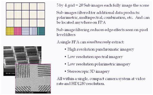
FIGURE 4-5 Description of an optical diversity imager.
but the full image can be recreated under certain constraints.54 This is an active area of research, as a natural extension of data compression approaches.
Because of this interest, DARPA has initiated a program called Large Area Coverage Optical Search-while-Track and Engage (LACOSTE). The idea was to develop extremely wide field-of-view coded aperture imaging technology to support single-sensor day-night persistent tactical surveillance of all moving vehicles in a large urban battlefield. LACOSTE-coded aperture imaging technology focused on achieving a very wide instantaneous field of regard using multiple simultane-
ous wide field-of-view (FOV) images.55,56,57,58,59,60,61,62,63,64,65,66 In coded apertures, a structured mask of pinhole cameras is created such that the image from each individual pinhole falls across a common FPA. With a large-area mask centered above a small FPA, the pinhole camera structure opens as a lens in the desired look direction while the remainder of the mask remains opaque. Knowing the mask structure, the multiple images on the same focal plane are digitally deconvolved to form an image. This concept provides several unique and enabling features. Orthogonally coded masks allow multiple simultaneous images at arbitrary pointing angles. Grouping pinholes enables electronically switchable resolution. The coded aperture replaces optical gain with digital processing gain.
A critical enabling technology for LACOSTE was the adaptive pinhole mask
where each pixel is physically small and addressable (either independently or in spatially distributed orthogonal groupings) and has millisecond switching speed, sufficient MWIR transmittance, low power consumption, large-area manufacturability, and extremely low cost per pixel. Another issue is compensating for dispersion effects while still using the pinholes, since there is a desire to use this “camera” in a broadband imager.
Lensless Imaging
Most sensors detect an image by using optics to focus light onto a detector array. This is referred to as detecting in the image plane because you form an image in this plane conjugate to the object you are viewing. A lens can be used alternatively to take a Fourier transform of the input light.67 This converts the input from the pupil plane to the image plane. If the phase and amplitude of the light wave are known in the pupil plane, they can be digitally converted to the image plane by taking a Fourier transform. This is the essence of so-called lensless imaging. The major difficulty with detecting in the pupil plane, and digitally converting to the image plane, is that detectors are sensitive to the intensity of the impinging light. The carrier frequency of light is orders-of-magnitude too high a bandwidth for existing detectors to follow. The fact that optical detectors do not detect the phase of the carrier can be mitigated by guessing the phase and using an image sharpness metric to iteratively find values of phase across the pupil plane that will provide the sharpest image.68 For passive visible and IR sensors, this is the only option to obtain phases for lensless imaging because of the broadband nature of these imagers. Spatial variation in phase can be estimated using wavefront measurement devices, such as the Shack-Hartman device discussed above. Measurements by such a device can assist the initial estimate of phase.
To measure the phase of an optical wave, a second, coherent optical wave can be directed at the detector at the same time as the first wave. This is called heterodyne detection. If this is done, then phase and amplitude can be measured, so a Fourier transform can be taken. To measure the phase of the detected signal, the detector bandwidth must be high enough to measure the beat frequency between the local oscillator and the signal to be detected. This cannot be accomplished for most passive sensors because the bandwidth of the detected signal is much broader than the bandwidth of the detector. For narrow-band active sensors, heterodyne detection can be used. There is a technique called spatial heterodyne that allows the use of low
bandwidth with a spatially offset local oscillator.69 Spatial heterodyne measures the spatial variation of phase across an aperture. Temporal phase is not measured.
Lensless imaging may not be completely lensless. If the detector focal plane array is the size of the aperture being used, no optics will be required. It is however likely that for many applications the receive aperture will be larger than available FPAs. If the receive aperture is not the same size as the FPA to be used, a telescope will be required to adjust the size of the pupil plane image prior to detection.
Signal-to-noise and sampling considerations are different in the pupil plane than in an image plane. Bright point objects in the image plane are distributed across the full aperture in the pupil plane. For a diffraction-limited set of optics, the detector size in the image plane is set to optical diffraction limit. Oversampling occurs when the detector size is smaller than the diffraction limit. The field-of-view of a traditional image plane sensor is set by multiplying the pixel linear dimension by the number of detectors in that dimension. In the pupil plane, detector sampling is opposite. The maximum sensor FOV is set by the size of the detector, while the maximum resolution to be sampled is set by the full array width, the product of detector linear dimension times the number of detectors.
IMPROVED COOLERS
Thermoelectrics
Current commercial thermoelectric (TE) coolers can achieve a maximum ∆T of ~100-130 K below room temperature. An example of a current commercially available multistage TE cooler that achieves a maximum ∆T of ~133 K, as measured from room temperature, is Marlow Industries’ MI6030-01BC shown in Figure 4-6. At this extreme temperature difference, however, the module cannot dissipate any heat (i.e., the coefficient of performance [COP] is essentially zero). Maximum COP for this device at DT = 0, as reported by Marlow Industries, is ~0.03.
In contrast, single-stage thermoelectric devices can achieve COP values approaching 0.6-1.0; however, the maximum ∆T for these devices is only ~70 K. Again, at ∆Tmax no heat can be pumped, so TE coolers typically operate at cold side temperatures that are only a fraction of their maximum achievable ∆T.
Existing commercial TE coolers have a market in providing temperature stability and noise reduction or dark current reduction for detector systems that operate at or near room temperature. Current available TE coolers do not have sufficient cooling capacity to be used for systems that require operation at temperatures below ~200 K. However, several recent developments in thermoelectric materials
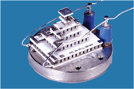
FIGURE 4-6 Marlow Industries’ MI6030-01BC. NOTE: The base dimensions are 21.84 × 28.19 mm. The module height is 20.73 mm. SOURCE: Marlow Industries, Inc., Subsidiary of II-VI Incorporated, 10451 Vista Park Rd, Dallas, TX 75238. Image available at http://www.marlow.com/thermoelectric-modules/six-stage/mi6030.html. Accessed March 25, 2010.
research suggest the potential for breakthroughs that may ultimately transform the use of TE coolers in detector systems. These developments include the demonstration of thin-film thermoelectrics with performance that is two to three times greater than conventional bulk materials at or near room temperature and new understandings of how nanostructurer can improve thermoelectric performance at cryogenic temperatures.
In 2001, Rama Venkatasubramanian and his colleagues at Research Triangle Institute (RTI) reported a significant breakthrough in the achievable figure of merit, ZT, in a thin-film superlattice of alternating bismuth telluride and antimony telluride materials. Based on the performance demonstrated, it is projected (see Figure 4-7) that the achievable COP for a TE cooler could approach or even exceed that of small-scale mechanical systems. In addition, the thin-film format allows for a much smaller-profile device for comparable performance compared to existing TE coolers (see Figure 4-8).
The potential for thin-film TE coolers for use in current and future detectors that operate near room temperature remains speculative. There are challenges with manufacturing, reliability, cost, and scale-up that still need to be overcome.
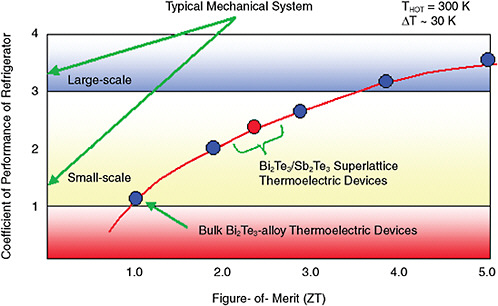
FIGURE 4-7 Achievable figure of merit, ZT, in a thin-film superlattice of alternating bismuth telluride-antimony telluride materials. SOURCE: Rama Venkatasubramanian, and colleagues, RTI International, Research Triangle Park, N.C.
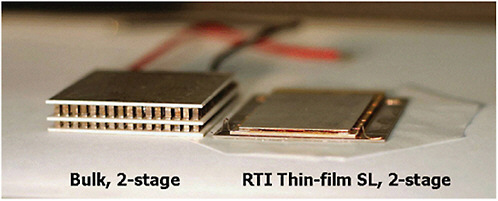
FIGURE 4-8 Advanced thin-film superlattice thermoelectric modules for FPA applications. NOTE: The bulk two-stage module—50 × 50 × 8 mm—versus the thin-film two-stage module—50 × 50 × 2.5 mm. The thin-film module has a factor of three advantage in module profile thickness and is significantly more lightweight, by a factor of 100 or more, for similar performance of heat pumping capacity. SOURCE: Rama Venkatasubramanian, and colleagues, RTI International, Research Triangle Park, N.C.
However, RTI has established a spinoff company, Nextreme Solutions, with the goal of commercializing its thin-film thermoelectric technology for a number of thermal management applications including hot spot management of microelectronic devices. According to Nextreme’s website (www.nextreme.com), it is able to provide samples of its thin-film thermoelectric coolers for evaluation by potential customers. Target applications include laser diodes, photodetectors, polymerase chain reaction (PCR), and light-emitting diodes (LEDs). While it does not appear that these coolers have currently achieved large-volume commodity status, Nextreme does report commercial shipments of some of its cooler products as having been initiated in 2009. The next several years will be critical in determining the long-term viability of this technology. Nextreme’s success or failure will likely determine the near-term opportunities for achieving significant breakthroughs in reduced size, weight, and power for the active cooling component of detectors that operate near room temperature.
A recent development reported up to a 100 percent enhancement in lead telluride compounds at 773 K by doping to create “resonant states.”70 This approach may be ideal for enhancing the thermoelectric performance of materials at cryogenic temperatures. If thermoelectric materials could be realized at cryogenic temperatures with ZT values in the range of 1-2, then it is conceivable that solid-state refrigerators could replace current mechanical cryocoolers. This could easily lead to an order-of-magnitude or more reduction in overall system weight and/or power requirements. The results are very preliminary, and there is comparatively little (compared to funding for TE power generation) funded research to specifically address thermoelectric development for cryogenic temperatures.
FINDING 4-6
Thin-film thermoelectric devices have the potential to substantially reduce size, weight, and power requirements of the active cooling component for room-temperature focal plane arrays. If these devices can meet cost and life-time metrics, they will displace the currently used bulk coolers. The near-term driver for these developments likely will be in fields such as microelectronics with much larger market potential than detectors.
RECOMMENDATION 4-1
The intelligence community should monitor commercial developments in thin-film cooler technology.
Phononic Crystals for Cooling
Work is under way in the area of silicon phononic crystal-based thermoelectric active cooling modules. The device concept is based on planar phononic crystal topologies that have the potential to surpass silicon nanowires in thermoelectric performance from both practical and scientific points of view. An approach that would permit the hybrid use of nano-patterning, quantum confinement, and coherent and incoherent scattering mechanisms for phonons in a mass producible setting, while at the same time leaving the electrical properties of silicon unaltered, can be achieved via the so-called phononic crystal (PnC) lattice. A PnC is a periodic arrangement of Mie scattering centers in a host matrix. 2-D planar phononic crystals have some significant advantages over nanowire topologies. The flexible nature of the 2-D phononic crystal topology could allow one to uniquely tailor the electronic structure of the silicon to facilitate improved Seebeck coefficients over those of nanowire topologies. 2-D PnC topologies have the potential to surpass silicon nanowires in thermoelectric performance from both practical and scientific points of view. Due to their improved mechanical strength, their larger contactable areas, reduced phononic thermal transport, and somewhat tailorable Seebeck coefficient, a 2-D PnC approach has a number of distinct advantages for creating thermoelectrics in a silicon platform. In addition to nanometer-geometry boundary scattering, PnC topologies will exhibit coherent Bragg scattering and reductions in group velocity that reduce phonon mobility beyond boundary scattering alone. Additionally, the flexible nature of the 2-D phononic crystal topology could allow one to uniquely tailor the electronic structure of the silicon to facilitate improved Seebeck coefficients over those of nanowire topologies.71,72
Laser Cooling
Laser cooling refers to one of several mechanisms by which laser light interacts with matter in a way that results in a net reduction in temperature. The reduction in temperature is associated with absorption and emission processes that result in a net loss of momentum at the atomic or molecular level. The most common form of laser cooling is Doppler cooling. Doppler cooling is a technique used to cool, low-density elemental gases (Cs, Rb, Na, etc.) to extremely low temperatures. The original motivation for developing techniques for cooling gases to temperatures of
hundreds of microkelvins or less was to improve the accuracy of atomic clocks as well as to explore the quantum mechanical nature of atomic physics.
Doppler cooling is observed when an atom is moving towards a laser light source. Under certain conditions, the atom can preferentially absorb photons with an energy that is slightly below a particular atomic resonance. In absorbing these photons, conservation of momentum requires the atom to slow its momentum in the direction opposite to the incident photon. As the atom relaxes back to its lower state, a photon is emitted in a random direction. The randomization of the atom’s momentum results in a net slowing of the atom’s motion and, therefore, a lowering of temperature.
The demonstration that Doppler cooling could successfully be used to achieve sub-millikelvin temperatures in elemental gases was acknowledged with a Nobel Prize in 1997 that was shared among Steven Chu, Claude Cohen-Tannoudji, and William D. Phillips.
Doppler cooling continues to be a useful research tool for exploring quantum physics and has found practical use in advanced inertial navigational systems. However, it is unlikely that this technology would be of value for sensor applications. It is a technique best suited to cooling gases as opposed to solids, and the achievable temperatures are well below the operating temperatures required for detector systems.
More recently, laser cooling based on the physics of anti-Stokes fluorescence has been demonstrated to result in substantial cooling of certain rare earth materials. In anti-Stokes fluorescence cooling, a solid absorbs photons at a particular frequency and then reemits at a higher frequency. The frequency shift results in a net loss of energy in the form of heat from lattice vibrations (phonons). This effect was first reported in 1995 by researchers from Los Alamos who observed a 0.3 K reduction in temperature in Yb3+-doped fluorozirconate glass.73 More recently, Seletskiy et al. have reported a record 155 K temperature reduction in ytterbium-doped LiYF4 using laser cooling.74 This exceeds the ∆T achievable using current state-of-the-art solid-state thermoelectric cooling technologies and represents a promising breakthrough for achieving a practical laser cooling capability.
This research is still at a very early stage, and there are few data on which to base a prediction of achievable coefficient of performance in a practical device. The technology would have the benefit of being solid state (no moving parts), so it could be of benefit to future detector systems where noise due to vibration is of concern. However, understanding the potential for achieving greater ∆T and reasonable coefficient of performance remains a significant challenge for this technology, which is still a very new and immature field of research.
ENHANCED SIGNAL PROCESSING
Key technology advancements in electronics and electronic devices have allowed for a previously unseen level of systems integration and miniaturization in IR sensors. Advancements in analog-to-digital converters, field-programmable gate arrays, and very small outline packaging have allowed IR systems to go from large multicard line-replacable units (LRUs), a complex component of a vehicle that can be replaced quickly at the organizational level, to battery-operated helmet-mounted devices over the last 15 years.
As shown in Figure 4-9, processing technologies that support both data and information transmission, as well as information and knowledge extraction, will be vital to future detector technologies. When a technological concept is reduced to practice, various design factors are traded against each other to achieve a new capability within constraints imposed by other elements of the system or to achieve a new capability as a consequence of a breakthrough removing a constraint elsewhere in the system. As a specific example of a constraint, remote sensing architectures will inevitably be constrained by the communications capabilities available to move data from the sensor system to processing or archival sites. On the other hand, the emergence of single-chip multicore processor architectures may allow significant local pre-processing of sensor data before they are transmitted from the remote sensor, reducing the bandwidth required and allowing the use of sensors with improved precision (e.g., the number of pixels in a focal plane array) or higher scan rates, each of which may be valuable in some applications.
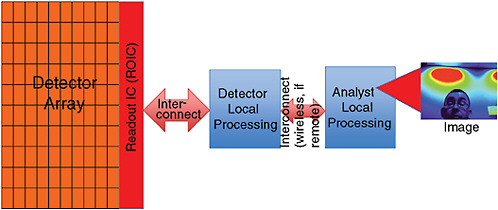
FIGURE 4-9 A high-level model that demonstrates the methodology and constraints involved with data and information transmission and information and knowledge extraction.
Data and Information Transmission
The major challenges facing data and information transmission are primarily at remote collector or sensing platforms. These challenges are distinct for close-in platforms, such as unattended ground sensors (UGS) and remote platforms (such as airborne and space). Both close-in and remote platforms have limited communication bandwidth; however, close-in platforms have additional severe constraints on power consumption. Once the raw data or derived information have reached the ground processing station, there are fewer limitations in terms of power requirements, computer power, and communication bandwidth. The technologies that address data transmission limitations on communication bandwidth belong to two major classes: (1) data compression and (2) data screening.
Data Compression
Lossless Compression Techniques A number of methods are aimed at achieving lossless compression;75,76,77,78,79 however, lossless compression can only a achieve a modest degree of compression. For example, an ARGUS-IS-like system can produce up to 770 gigabits per second. The use of a Common Data Link (CDL) operating at 274 megabits per second would require compression ratios on the order of 2,800, far beyond the capabilities of lossless compression techniques.
Lossy Compression Techniques Most lossy compression80 methods include three major steps: (1) signal decomposition-transformation, (2) quantization-thresholding, and (3) encoding. The first step is focused on transforming the signal into a representation that can be compressed more efficiently by reducing dynamic range, removing redundancy, among other things. This step is also taken by many lossless techniques and is reversible. Commonly-used transforms include discrete cosine transform (DCT)81 and discrete wavelet transform (DWT).82 The quantization step that follows the signal transformation is the step that reduces the number of output symbols and is the source of information loss and also encoding-
|
75 |
Available at http://en.wikipedia.org/wiki/Run-length_encoding. |
|
76 |
Available at http://en.wikipedia.org/wiki/DPCM. |
|
77 |
Available at http://en.wikipedia.org/wiki/Predictive_Coding. |
|
78 |
Available at http://en.wikipedia.org/wiki/Entropy_encoding. |
|
79 |
Available at http://en.wikipedia.org/wiki/LZW. |
|
80 |
Lossy compression reduces the size of the file required to store information but does not save all of the original information. |
|
81 |
N. Ahmed, T. Natarajan, and K.R. Rao. 1974. Discrete cosine transform. IEEE Transactions on Computers C-23:90-93. |
|
82 |
M. Vetterli and J. Kovacevic. 1995. J. Wavelets and Subband Coding. Englewood Cliffs, N.J.: Prentice Hall. |
compression efficiency. The last step of encoding is aimed at achieving rates that approach the entropy of the quantized values or symbols.83
Emerging Compression Techniques Compressive sensing or sampling is an emerging technology that is surfacing in various implementations ranging from a direct application of image compression to new sensors that embed the concept of compressed sensing at the analog-optical layer.84 Compressive sensing or sampling relies on two basic principles, sparsity and incoherence. The basic assertion is that many signals are sparse, meaning that they have a very compact representation if the basis functions are chosen properly. Incoherence is an extended case of the duality concept between time and frequency domains, sparse in time and spread in frequency. If the signal has a compact representation in some basis, the sampling-sensing waveforms have a very dense representation. The implication is that we can design efficient sampling that captures the useful information embedded in the signal and transforms it into a small amount of data. Large upfront data reduction directly translates to a reduced requirement for communication bandwidth. The simplicity of the sampling stage is obtained at the cost of a complex reconstruction stage that requires the application of computing-intensive linear programming techniques.
The same concepts are also being explored in the design of a new generation of imagers that employ compressive sensing at the optical-analog layer. In this new concept of sensing a smaller number of measurements is acquired, and each measurement corresponds to a quantity in the transformed space that is optically accomplished as the inner product of the scene with the basis functions. Because of the significant reduction of sensor components and elements (without sacrifice in performance), these new imagers likely will be deployed on many more platforms than currently feasible.
|
83 |
Entropy is considered a standard measure of complexity. It is a property of a distribution over a discrete set of symbols. For a sequence {i} of symbols x drawn from an alphabet with a probability p(i), the entropy H(i) of the random variable I is given by H(i) = S p(i) log2 p(i). The units of entropy and entropy rate defined above are bits and bits per symbol. The entropy of a sequence is the length of shortest binary description of the states of the random variable that generates the sequence, so it is the size of the most compressed description of the sequence. For additional information, see S. Lloyd. 1990. Physical measures of complexity. In E. Jen, ed. 1989 Lectures in Complex Systems, SFI Studies in the Sciences of Complexity, Vol. II, pp. 67-73. Addison-Wesley; Claude E. Shannon. 1948. A mathematical theory of communication, Bell System Technical Journal 27:379-423, 623-656. There is a related measure of complexity, called Kolmogorov complexity, that measures the size of the smallest program necessary to produce an output. For additional information, see http://en.wikipedia.org/wiki/Entropy_(information_theory. Last accessed June 21, 2010. |
|
84 |
Emmanuel J. Candès and Michael B. Wakin. 2008. An introduction to compressive sampling. IEEE Signal Processing Magazine 13(March). |
Data Screening Techniques
The basic principle behind the application of data screening methods is to filter (screen) the raw data and extract only the data segments that are of interest. This is called relevance filtering in other contexts. Example screening techniques include automatic target detection and/or recognition and material identification, among others. In principle, the use of data screening techniques as a compression mechanism amounts to shifting the specific mission processing algorithms from the receiving ground station to the collection platform. A number of approaches can be taken once the image regions of interest have been identified. One approach is to transmit only the data associated with the regions of interest (with no loss of fidelity) and discard the remaining data. However one might choose to further reduce the volume of data either through lossy compression of the selected data or the use of derived attributes such as the identification and location of the detected targets. This compression method is typically used in unmanned ground sensors, as well as on some airborne platforms.
Application-specific Processing
The signal processing and exploitation chain consists of two major components; (1) conversion of sensor input into physical meaningful values that then can be further processed by (2) mission- or application-specific algorithms (e.g., missile detection and tracking, target detection, automatic target recognition, and material identification). In this report the primary focus is on the core signal processing chain that is accomplished on the collection platform and is essential for high-quality image acquisition, as shown in Figure 4-10.
In the IR and high-performance visible imaging area, fully digital focal planes are just entering the market. In some cases their performance exceeds that of traditional analog focal planes coupled to discrete electronics. On-ROIC digital logic enables future digital signal processing such as nonuniformity correction (NUC), image stabilization, and compression leading to much smaller systems (microsystems). This technology is poised to go into large-area cryogenic infrared sensors over the next few years.
Local Processing
Sending data off-chip requires substantial power, and sending those data through communication links (for example, an RF link for an unattended ground sensor) is even more energy intensive. As described above, most of the basic functionality depicted in Figure 4-10 such as AGC (automatic gain control) and TDI time delay integration is currently embedded and implemented as an integral part of the ROIC functionality. There is increasing recognition of the value of trying to
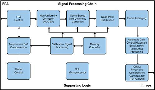
FIGURE 4-10 Components of a signal processing architecture.
identify and transmit only small amounts of high-level “actionable information” rather than large numbers of raw data bits.
Architectural bottlenecks occur when steps in digital signal processing are mismatched in their performance. The goal of later processing steps should be to extract as much information as possible from this sensing infrastructure. In practice this means processing to remove noise, to obtain true information, and to lose as little information as possible. A bottleneck in a system can be viewed as a lossy filter. In the case of a parallel front end, it will have a number of bits of attributes, such as amplitudes, but perhaps frequencies and phases as well, available to late processing stages. For example, for a 10-megapixel array, each pixel might produce 32 bits of information per sample at a sampling rate of 30 frames per second, leading to an aggregate “bit rate” of 9.6 × 10⁹, or about 1.2 gigabytes, per second. More information per sample, more pixels, or a greater scan rate has a significant effect on the processing and communication demands of such a sensor.
As a specific example, the DARPA ARGUS-IS unmanned aerial system described in Chapter 3 (Boxes 3-1 and 3-2) contains 368 visible FPAs.85 At data rates
of 96 megapixels per second per FPA, 12 bits per pixel, and 368 FPAs, the total data rate from the sensor is about 424 gigabits per second. This data rate is beyond the capacities of conventional processing elements. In addition, ARGUS-IS uses a spread-spectrum jam-resistant CDL wireless data link of 274 megabit per second capacity. If the wireless data link is fully utilized, the on-board systems must achieve a data rate reduction of 423,936/274 or more than 1,500, which is difficult to achieve with compression technologies alone.
ARGUS-IS approaches the data management challenge with a novel on-board processing architecture, characterized by parallel interconnects. Each FPA pair feeds a field-programmable gate array (FPGA) that multiplexes the data from the two FPAs (a total of 2.3 gigabits per second), time tags these data, and interleaves the data onto a fiber-optic transceiver. The transceiver is a commercial off-the-shelf (COTS) device operating at 3.3 gigabits per second. Sixteen 12-fiber ribbon cables connect the 184 FPGA pairs to the ARGUS-IS airborne processor system, a multiprocessor system illustrated in Box 3-1, which consists of 32 processor modules. Each processor module can handle 6 fibers, or about 20 gigabits per second of data, and consists of two Xilinx Virtex 5 FPGAs and a low-power Intel Pentium general-purpose central processing unit (CPU).
The ARGUS-IS designers believe that the processor modules can provide more than 500 billion operations per second each, for a total processing capacity for the 32 processor modules in excess of 16 trillion operations per second. To overcome some of the data rate limitations of the CDL downlink, JPEG 2000 compression is done using application-specific integrated circuits (ASICs) to provide hardware assist. The ARGUS-IS designers note the severe limitations of the 200+ megabit per second data link and propose moving target tracking into the on-board software. ARGUS-IS illustrates many of the system architecture trade-offs discussed in this chapter.
As the demand is increasing for on-board processing functionality that mirrors what traditionally has been accomplished on the ground, the need for compute power that meets size, weight, and power (SWaP) constraints is continuously growing. The amount of processing that can be placed right at the pixel has generally been limited by the modest numbers of transistors that can be placed within a small pixel.
Significant advances have been made in computer architectures and are currently referred to as high-performance computing. Commercial applications such as video gaming, increased cell phone functionality, and so forth, have been pushing significant advances in small, low-power, high-performance computing platforms
that are available on the commercial market (for example, multicore processors and multicore graphics processing units [GPUs]) and have no International Traffic in Arms Regulations (ITAR) restrictions. Figure 4-11 depicts a Texas Instruments system-on-the-chip solution for cell phone applications. The significant advances in high-performance computing over the last decade are making real-time on-board processing a reachable reality.
However, the complexity of programming these powerful processors and achieving their potential computer power has significantly increased—both the exploitation of the available parallelism and the memory organization of the computation are subtle and require significant effort. A key enabler for exploiting this emerging computational power is the new sets of software tools that enable rapid porting and debugging of existing algorithms into multicore computing platforms. As discussed in the following two examples, extensive sets of dedicated software tools are emerging in support of the hardware platforms.
FIGURE 4-11 Texas Instruments OMAP 4430 system on a chip. SOURCE: Courtesy Texas Instruments. Available at http://focus.ti.com/general/docs/wtbu/wtbuproductcontent.tsp?templateId=6123&navigationId=12843&contentId=53243. Last Accessed March 25, 2010.
NVIDIA multicore technology is one example of commercially available highperformance computing technologies. In 2010, NVIDIA announced the launch of its next generation Tegra, a multiprocessing system focused on the mobile web.86 The Tegra has eight independent processors, including a dual-core CPU for mobile applications. These processors are used together or independently to optimize power usage.
At another point on the performance scale, NVIDIA has also introduced the capability to perform petascale computing with teraflop processors. The NVIDIA Tesla C1060 computing processor provides energy-efficient parallel computing power by bringing the performance of a small cluster to a workstation environment. The CUDA programming environment (“C” programming language, enhanced with thread management primitives to inform the runtime for the GPU of what can be executed concurrently) simplifies the development of applications for its multiple 240-core processors.
Another example that has a significantly lower power profile is the series of multicore chips and boards provided by Tilera. The first generation Tilera TILE64 commercial chip is laid out as an 8 tile × 8 tile interconnect using a pipe-lined and programmable two-dimensional, proprietary, high-performance, low-latency mesh. The mesh can transport streams of data, memory blocks, or scalar values, adding to the flexibility of the programming models available for the chip. In addition, this approach can support arbitrary numbers of tiles, so that 8 × 8 in this initial chip is not a fixed configuration. This makes the architecture particularly suitable for radiation hard applications where a different number of tiles per chip may be required for power dissipation and several other technical reasons. The switch engine in each tile completely offloads the tile processing engine from iMesh™ netork routing and protocol handling, and provides buffering and flow control so that tiles can perform processing in an asynchronous manner. Each network link is full duplex. The dynamic networks are routed in a tile-layout fashion (x-direction first, then y-direction). A RadHard by design chip (MAESTRO) is currently being developed under the National Reconnaissance Office-funded OPERA program.
The third generation of Tilera Corporation’s multicore processor is aimed at delivering the highest available general-purpose compute at the lowest power consumption. The TILE100 will provide a 4× to 8× increase in performance over Tilera’s current TILEPro64 processor and will double the performance-per-watt metric. Table 4-2 provides a comparison between the Tile64, the Tile100, and the MAESTRO processors.
TABLE 4-2 Comparison Between the Tile64, the Tile100, and the RadHard by Design Processors
|
Performance |
TILEPro64 |
Tile100 (Greylock) |
Maestro (RHBD) |
|
Number of cores |
64 |
100 |
49 |
|
Temperature range |
0°C-70°C |
0°C-70°C |
−55°C-125°C |
|
Foundry |
TSMC |
TSMC |
IBM |
|
Feature size |
90 nm |
40 nm |
90 nm |
|
On-chip cache (MB) |
5.6 |
32 |
4.3 |
|
Floating point operations (GFLOPS) |
~10 (software emulated) |
29 (FPU accelerator) |
22 (IEE 754 FPU per each core) |
|
On-chip bandwidth (Tbit/s) |
38 |
232 |
16 |
|
Clock speed (MHz) |
700, 866 |
1250, 1750 |
300 |
|
Typical power (W) |
27 |
<50 (estimated) |
18 (estimated) |
|
Total I/O bandwidth (Gbps) |
40 |
44 |
40 |
|
Ethernet bandwidth |
2 XAUI, 2GbE |
2 XAUI, 2GbE |
4 XAUI, 4GbE |
|
NOTE: FPU = floating point unit; I/O = input-output. SOURCE: Data derived from http://www.tilera.com/products/TILEPro64.php; http://www.tilera.com/products/TILE-Gx.php; http://nepp.nasa.gov/mapld_2009/talks/083109_Monday/03_Malone_Michael_mapld09_pres_1.pdf. Accessed March 25, 2010. |
|||
Tilera provides a Multicore Development Environment (MDE). The MDE tool kit provides a complete Integrated Development Environment (IDE).87
FINDING 4-7
Scaling the data throughput of focal plane sensor systems involves not only the sensor chip but also the detector-processor interface, signal processing and compression, and the communication link (wireless for remote air- and space-borne missions). Advanced compression and filtering with on-board processing provided by commodity multicore architectures are reducing communications demands.
RECOMMENDATION 4-2
Analyses of national capabilities should include consideration of advances in processing technologies for other uses—for example, commercial developments—that could also enhance the use of detectors in future sensor systems.
Multisensor Data Fusion
Performance enhancements can be achieved when combining data collected with IR sensors with additional sensor modalities. Multisensor data fusion88,89,90 has been an evolving set of architectures and algorithms for drawing inferences from a multiplicity of sensors used in combination. Any given multisensory system will have an architecture that defines its ultimate capabilities, and then a set of algorithms will be used to draw the necessary inferences from the fused data. Algorithms for sensor fusion include techniques such as Bayesian inference,91 Dempster-Shafer 92,93 evidential reasoning, and voting. The specific techniques depend on both the mission or application and the specific sensor modalities. Sample applications include image enhancement for improved navigation in low-light conditions, target detection, and target recognition. An example is the fusion of data from a pulsed radar and an IR sensor, as shown in Figure 4-12.94 The radar can determine range, but not angular direction, while the forward-looking infrared (FLIR) can determine angular direction, but not range. By fusing the two sensor modalities, both range and angular direction can be determined.
Three specific methods for sensor fusion include raw data fusion, feature-level fusion, and decision-level fusion. The highest level of fusion occurs when the multiple images are combined into a single multivalue image that is then exploited. This requires accurate alignment of sensor measurements across the multiple sensors resulting in a vector of multimodal measurements associated with a common ground location. The combined multivalue image is then processed by an application-specific algorithm, such as automatic target cuing-recognition
FIGURE 4-12 Fusion of data from a pulsed radar and an IR sensor. SOURCE: David L. Hall and James Llinas. 1997. An Introduction to multisensory data fusion. Proc. IEEE 85(1).
(ATC/R), that simultaneously operates on the vector of measurements. Fusion techniques that operate in this mode are known as raw data fusion as well as centralized data fusion methods, and they typically assume a common image projection plane for the multiple sensors. Multi- and hyperspectral sensors are well matched for this type of fusion approach.95,96 Centralized data fusion is not typically applied to sensors that do not share a common imaging plane such as synthetic aperture radar (SAR).97
FIGURE 4-13 Improved ATC through feature-level fusion of SAR and multispectral imagery. SOURCE: T. Peli, M. Young, R. Knox, Ellis, K., and F. Bennett. 1999. Feature level fusion. Proc. SPIE Sensor Fusion: Architecture, Algorithms and Applications III, Vol. 3719. Orlando, Fla.
In contrast to raw data fusion, feature- and decision-level fusion methods do not require precise alignment. In a decision-level fusion, also known as distributed data fusion, an independent decision is made based on a single data modality and the decisions are passed to the fusion node where a global decision is made using a variety of algorithms including Bayesian inferencing. Feature-level fusion is a hybrid between raw data fusion and decision-level fusion. In feature-level fusion,98 each sensor output is processed independently, and attributes associated with events or entities of interest that have been extracted in each sensor domain are combined and a decision is made based on the joint feature set. Figure 4-13 depicts improved ATC/R through feature level fusion of SAR and multispectral imagery.
CONCLUDING THOUGHTS
Emerging technologies could enable new capabilities, with examples being the ability of some advanced detector technologies to enable multispectral sensing through a single aperture and the potential advantages in selectivity accruing from nanophotonics. Advances in non-detector-specific technologies, such as communications technology and signal processing technologies, have a direct bearing on the ability to turn detector data into useful information. As an example, the effects of miniaturization and parallel processing have made commodity components
sufficiently powerful to provide onboard processing capabilities for a gigapixel capability.
Both the basic science underlying advances in detectors, optics, coolers, and algorithms and the commodity processing capabilities enabling new trades in signal processing are available worldwide. Emerging detector and related system-level technologies have significant potential for advancing sensor systems and deserve attention from the intelligence community in assessing present and future global sensor system capabilities.


