
3
Power Is Now Limiting Growth in Computing Performance
The previous chapters define computer performance and discuss why its continued growth is critical for the U.S. economy. This chapter explores the relationship between computer performance and power consumption. The limitations imposed by power consumption are responsible for the present movement toward parallel computation. This chapter argues that such limitations will constrain the computation performance of even parallel computing systems unless computer designers take fundamentally different approaches.
The laws of thermodynamics are evident to anyone who has ever used a laptop computer on his or her lap: the computer becomes hot. When you run a marathon, your body is converting an internal supply of energy formed from the food you eat into two outputs: mechanical forces produced by your body’s muscles and heat. When you drive your car, the engine converts the energy stored in the gasoline into the kinetic energy of the wheels and vehicle motion and heat. If you put your hand on an illuminated light bulb, you discover that the bulb is not only radiating the desired light but also generating heat. Heat is the unwanted, but inevitable, side effect of using energy to accomplish any physical task—it is not possible to convert all the input energy perfectly into the desired results without wasting some energy as heat.
A vendor who describes a “powerful computer” is trying to characterize the machine as fast, not thermally hot. In this report, the committee uses power to refer to the use of electric energy and performance to mean computational capability. When we refer to power in the context of a
computer system, we are talking about energy flows: the rate at which energy must be provided to the computer system from a battery or wall outlet, which is the same as the rate at which that energy, now converted to heat, must be extracted from the system. The temperature of the chip or system rises above the ambient temperature and causes heat energy to flow into the environment. To limit the system’s temperature rise, heat must be extracted efficiently. (Transferring heat from the computer system to the environment is the task of the cooling subsystem in a computer.) Thus, referring to a chip’s power requirements is equivalent to talking about power consumed and dissipated.
When we talk about scaling computing performance, we implicitly mean to increase the computing performance that we can buy for each dollar we spend. If we cannot scale down the energy per function as fast as we scale up the performance (functions per second), the power (energy per second) consumed by the system will rise, and the increase in power consumption will increase the cost of the system. More expensive hardware will be needed to supply the extra power and then remove the heat that it generates. The cost of managing the power in and out of the system will rise to dominate the cost of the hardware.
Historically, technology scaling has done a good job of scaling down energy cost per function as the total cost per function dropped, and so the overall power needs of systems were relatively constant as performance (functions per second) dramatically increased. Recently, the cost per function has been dropping faster than the power per function, which means that the overall power of constant-cost chips has been growing. The power problem is getting worse because of the recent difficulty in continuing to scale down power-supply voltages, as is described later in this chapter.
Our ability to supply power and cool chips is not improving rapidly, so for many computers the performance per dollar is now limited by power issues. In addition, computers are increasingly available in a variety of form-factors and many, such as cell phones, have strict power limits because of user constraints. People do not want to hold hot cell phones, and so the total power budget needs to be under a few watts when the phone is active. Designers today must therefore find the best performance that can be achieved within a specified power envelope.
To assist in understanding these issues, this chapter reviews integrated circuit (IC) technology scaling. It assumes general knowledge of electric circuits, and some readers may choose to review the findings listed here and then move directly to Chapter 4. The basic conclusions of this chapter are as follows:
- Power consumption has become the limiting constraint on future growth in single-processor performance.
- Power limitations on individual processors have resulted in chips that have multiple lower-power processors that, in some applications, yield higher aggregate performance than chips with single power-limited processors.
- Even as the computing industry successfully shifts to multiple, simpler, and lower-power processor cores per chip, it will again face performance limits within a few years because of aggregate, full-chip power limitations.
- Like complementary metal oxide semiconductor (CMOS) transistors, many of the electronic devices being developed today as potential replacements for CMOS transistors are based on regulating the flow of electrons over a thermodynamic barrier and will face their own power limits.
- A promising approach to enabling more power-efficient computation is to design application-specific or algorithm-specific computational units. For that approach to succeed, new chip design and verification methods (such as advanced electronic-design automation tools) will need to be developed to reduce the time and cost of IC design, and new IC fabrication methods will be needed to reduced the one-time mask costs.
- The present move to chip multiprocessors is a step in the direction of using parallelism to sustain growth in computing performance. However, this or any other hardware architecture can succeed only if appropriate software can be developed to exploit the parallelism in the hardware effectively. That software challenge is the subject of Chapter 4.
For intrepid readers prepared to continue with this chapter, the committee starts by explaining how classic scaling enabled the creation of cheaper, faster, and lower-power circuits; in essence, scaling is responsible for Moore’s law. The chapter also discusses why modern scaling produces smaller power gains than before. With that background in technology scaling, the chapter then explains how computer designers have used improving technology to create faster computers. The discussion highlights why processor performance grew faster than power efficiency and why the problem is more critical today. The next sections explain the move to chips that have multiple processors and clarify both the power-efficiency advantage of parallel computing and the limitations of this approach. The chapter concludes by mentioning some alternative technologies to assess the potential advantages and the practicality of these approaches. Alternatives to general-purpose processors are examined as a way to address
power limitations. In short, although incremental advances in computing performance will continue, overcoming the power constraint is difficult or potentially impossible and will require radical rethinking of computation and of the logic gates used to build computing systems.
BASIC TECHNOLOGY SCALING
Although this report focuses on computers based on IC processors, it is useful to remember that computers have historically used various technologies. The earliest electric computers were built in the 1940s and used mechanical relays.1,2 Vacuum tubes enabled faster electronic computers. By the 1960s, the technology for building computers changed again, to transistors that were smaller and had lower cost, lower power, and greater reliability. Within a decade, computers migrated to ICs instead of discrete transistors and were able to scale up performance as the technology scaled down the size of transistors in the ICs. Each technology change, from relays to vacuum tubes to transistors to ICs, decreased the cost, increased the performance of each function, and decreased the energy per function. Those three factors enabled designers to continue to build more capable computers for the same cost.
Early IC computers were built with bipolar transistors3 in their ICs, which offered high performance but used relatively high power (compared with other IC options). By the late 1970s, low-end computers used NMOS4 technology, which offered greater density and thus lower cost per function but also lower-speed gates than the bipolar alternative. As scaling continued, the cost per function was dropping rapidly, but the energy needs of each gate were not dropping as rapidly, so the power-dissipation
__________________________
1Raúl Rojas, 1997, Konrad Zuse’s legacy: The architecture of the Z1 and Z3, IEEE Annals of the History of Computing 19(2): 5-19.
2IBM, 2010, Feeds, speeds and specifications, IBM Archives, website, available online at http://www-03.ibm.com/ibm/history/exhibits/markI/markI_feeds.html.
3Silicon ICs use one of two basic structures for building switches and amplifiers. Both transistor structures modify the silicon by adding impurities to it that increase the concentration of electric carriers—electrons for N regions and holes for P regions—and create three regions: two Ns separated by a P or two Ps separated by an N. That the electrons are blocked by holes (or vice versa) means that there is little current flow in all these structures. The first ICs used NPN bipolar transistors, in which the layers are formed vertically in the material and the current flow is a bulk property that requires electrons to flow into the P region (the base) and holes to flow into the top N region (the emitter).
4NMOS transistors are lateral devices that work by having a “gate” terminal that controls the surface current flow between the “source” and “drain” contacts. The source-drain terminals are doped N and supply the electrons that flow through a channel; hence the name NMOS. Doping refers to introducing impurities to affect the electrical properties of the semiconductor. PMOS transistors make the source and drain material P, so holes (electron deficiencies) flow across the channels.
requirements of the chips were growing. By the middle 1980s, most processor designers moved from bipolar and NMOS to CMOS5 technology. CMOS gates were slower than those of NMOS or bipolar circuits but dissipated much less energy, as described in the section below. Using CMOS technology reduced the energy per function by over an order of magnitude and scaled well. The remainder of this chapter describes CMOS technology, its properties, its limitations, and how it affects the potential for growth in computing performance.
CLASSIC CMOS SCALING
Computer-chip designers have used the scaling of feature sizes (that is, the phenomenon wherein the same functionality requires less space on a new chip) to build more capable, more complex devices, but the resulting chips must still operate within the power constraints of the system. Early chips used circuit forms (bipolar or NMOS circuits) that dissipated power all the time, whether the gate6 was computing a new value or just holding the last value. Even though scaling allowed a decrease in the power needed per gate, the number of gates on a chip was increasing faster than the power requirements were falling; by the early to middle 1980s, chip power was becoming a design challenge. Advanced chips were dissipating many watts;7 one chip, the HP Focus processor, for example, was dissipating over 7 W, which at the time was a very large number.8 Fortunately, there was a circuit solution to the problem. It became possible to build a type of gate that dissipated power only when the output value changed. If the inputs were stable, the circuit would dissipate practically no power.
Furthermore, the gate dissipated power only as long as it took to get the output to transition to its new value and then returned to a zero-power state. During the transition, the gate’s power requirement was comparable with those of the previous types of gates, but because the transition lasts only a short time, even in a very active machine a gate
__________________________
5 The C in CMOS stands for complementary. CMOS uses both NMOS and PMOS transistors.
6 A logic gate is a fundamental building block of a system. Gates typically have two to four inputs and produce one input. These circuits are called logic gates because they compute simple functions used in logic. For example, an AND gate takes two inputs (either 1s or 0s) and returns 1 if both are 1s and 0 if either is 0. A NOT gate has only one input and returns 1 if the input is 0 and 0 if the input is 1.
7 Robert M. Supnick, 1984, MicroVAX 32, a 32 bit microprocessor, IEEE Journal of Solid State Circuits 19(5): 675-681, available online at http://ieeexplore.ieee.org/stamp/stamp.jsp?arnumber=1052207&isnumber=22598.
8 Joseph W. Beyers, Louis J. Dohse, Jospeh P. Fucetola, Richard L. Kochis, Cliffird G. Lob, Gary L. Taylor, and E.R. Zeller, 1981, A 32-bit VLSI CPU chip, IEEE Journal of Solid-State Circuits 16(5): 537-542, available online at http://ieeexplore.ieee.org/stamp/stamp.jsp?arnumber=1051634&isnumber=22579.
TABLE 3.1 Scaling Results for Circuit Performance
|
|
|
|
Device or Circuit Parameter |
Scaling Factor |
|
|
|
|
Device dimension tox, L, W |
1/k |
|
Doping concentration Na |
k |
|
Voltage V |
1/k |
|
Current I |
1/k |
|
Capacitance eA/t |
1/k |
|
Delay time per circuit VC/I |
1/k |
|
Power dissipation per circuit VI |
1/k 2 |
|
Power density VI/A |
1 |
|
|
|
SOURCE: Reprinted from Robert H. Dennard, Fritz H. Gaensslen, Hwa-Nien. Yu, V. Leo Rideout, Ernest Bassous, and Andre R. LeBlanc, 1974, Design of ion-implanted MOSFETS with very small physical dimensions, IEEE Journal of Solid State Circuits 9(5): 256-268.
would be in transition around 1 percent of the time. Thus, moving to the new circuit style decreased the power consumed by a computation by a factor of over 30.9 The new circuit style was called complementary MOS, or CMOS.
A further advantage of CMOS gates was that their performance and power were completely determined by the MOS transistor properties. In a classic 1974 paper, reprinted in Appendix D, Robert Dennard et al. showed that the MOS transistor has a set of very convenient scaling properties.10 The scaling properties are shown in Table 3.1, taken from that paper. If all the voltages in a MOS device are scaled down with the physical dimensions, the operation of the device scales in a particularly favorable way. The gates clearly become smaller because linear dimensions are scaled. That scaling also causes gates to become faster with lower energy per transition. If all dimensions and voltages are scaled by the scaling factor κ (κ has typically been 1.4), after scaling the gates become (1/κ)2 their previous size, and κ2 more gates can be placed on a chip of roughly the same size and cost as before. The delay of the gate also decreases by 1/κ, and, most important, the energy dissipated each time the gate switches decreases by (1/κ)3. To understand why the energy drops so rapidly, note that the energy that the gate dissipates is proportional to the energy that is stored at the output of the gate. That energy is proportional to a quan-
__________________________
9The old style dissipated power only half the time; this is why the improvement was by a factor of roughly 30.
10Robert H. Dennard, Fritz H. Gaensslen, Hwa-Nien. Yu, V. Leo Rideout, Ernest Bassous, and Andre R. LeBlanc, 1974, Design of ion-implanted MOSFETS with very small physical dimensions, IEEE Journal of Solid State Circuits 9(5):256–268.
tity called capacitance11 and the square of the supply voltage. The load capacitance of the wiring decreases by 1/κ because the smaller gates make all the wires shorter and capacitance is proportional to length. Therefore, the power requirements per unit of space on the chip (mm2), or energy per second per mm2, remain constant:
That the power density (power requirements per unit space on the chip, even when each unit space contains many, many more gates) can remain constant across generations of CMOS scaling has been a critical property underlying progress in microprocessors and in ICs in general. In every technology generation, ICs can double in complexity and increase in clock frequency while consuming the same power and not increasing in cost.
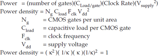
Given that description of classic CMOS scaling, one would expect the power of processors to have remained constant since the CMOS transition, but this has not been the case. During the late 1980s and early 1990s, supply voltages were stuck at 5 V for system reasons. So power density would have been expected to increase as technology scaled from 2 μm to 0.5 μm. However, until recently supply voltage has scaled with technology, but power densities continued to increase. The cause of the discrepancy is explained in the next section. Note that Figure 3.1 shows no microprocessors above about 130 W; this is because 130 W is the physical limit for air cooling, and even approaching 130 W requires massive heat sinks and local fans.
__________________________
11Capacitance is a measure of how much electric charge is needed to increase the voltage between two points and is also the proportionality constant between energy stored on a wire and its voltage. Larger capacitors require more charge (and hence more current) to reach a voltage than a smaller capacitor. Physically larger capacitors tend to have larger capacitance. Because all wires have at least some parasitic capacitance, even just signaling across the internal wires of a chip dissipates some power. Worse, to minimize the time wasted in charging or discharging, the transistors that drive the signal must be made physically larger, and this increases their capacitance load, which the prior gate must drive, and costs power and increases the incremental die size.
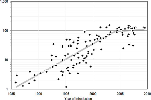
FIGURE 3.1 Microprocessor power dissipation (watts) over time (1985-2010).
HOW CMOS-PROCESSOR PERFORMANCE IMPROVED EXPONENTIALLY, AND THEN SLOWED
Microprocessor performance, as measured against the SPEC2006 benchmark12,13,14 was growing exponentially at the rate of more than 50 percent per year (see Figure 3.2). That phenomenal single-processor performance growth continued for 16 years and then slowed substantially15 partially because of power constraints. This section briefly describes how those performance improvements were achieved and what contributed to the slowdown in improvement early in the 2000s.
To achieve exponential performance growth, microprocessor designers scaled processor-clock frequency and exploited instruction-level paral-
__________________________
12For older processors, SPEC2006 numbers were estimated from older versions of the SPEC benchmark by using scaling factors.
13John L. Henning, 2006, SPEC CPU2006 benchmark descriptions, ACM SIGARCH Computer Architecture News 34(4): 1-17.
14John L. Henning, 2007, SPEC CPU suite growth: An historical perspective, ACM SIGARCH Computer Architecture News 35(1): 65-68.
15John L. Hennessy and David A. Patterson, 2006, Computer Architecture: A Quantitative Approach, fourth edition, San Francisco, Cal.: Morgan Kauffman, pp. 2-4.
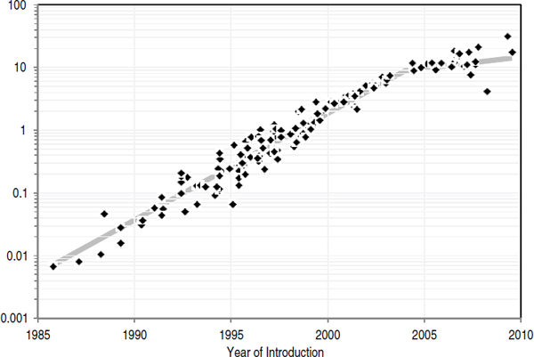
FIGURE 3.2 Integer application performance (SPECint2006) over time (1985-2010).
lelism (ILP) to increase the number of instructions per cycle.16,17,18 The power problem arose primarily because clock frequencies were increasing faster than the basic assumption in Dennard scaling (described previously). The assumption there is that clock frequency will increase inversely proportionally to the basic gate speed. But the increases in clock frequency were made because of improvements in transistor speed due to CMOS-technology scaling combined with improved circuits and architecture. The designs also included deeper pipelining and required less logic (fewer operations on gates) per pipeline stage.19
Separating the effect of technology scaling from those of the other improvements requires examination of metrics that depend solely on the improvements in underlying CMOS technology (and not other improve-
__________________________
16Ibid.
17Mark Horowitz and William Dally, 2004, How scaling will change processor architecture, IEEE International Solid States Circuits Conference Digest of Technical Papers, San Francisco, Cal., February 15-19, 2004, pp. 132-133.
18Vikas Agarwal, Stephen W. Keckler, and Doug Burger, 2000, Clock rate versus IPC: The end of the road for conventional microarchitectures, Proceedings of the 27th International Symposium Computer Architecture, Vancouver, British Columbia, Canada, June 12-14, 2000, pp. 248-259.
19Pipelining is a technique in which the structure of a processor is partitioned into simpler, sequential blocks. Instructions are then executed in assembly-line fashion by the processor.
ments in circuits and architecture). (See Box 3.1 for a brief discussion of this separation.) Another contribution to increasing power requirements per chip has been the nonideal scaling of interconnecting wires between CMOS devices. As the complexity of computer chips increased, it was not sufficient simply to place two copies of the previous design on the new chip. To yield the needed performance improvements, new commu-
BOX 3.1
Separating the Effects of CMOS Technology Scaling on Performance by Using the FO4 Metric
To separate the effect of CMOS technology scaling from other sorts of optimizations, processor clock-cycle time can be characterized by using the technology-dependent delay metric fanout-of-four delay (FO4), which is defined as the delay of one inverter driving four copies of an equally sized inverter.1,2 The metric measures the clock cycle in terms of the basic gate speed and gives a number that is relatively technology-independent. In Dennard scaling, FO4/cycle would be constant. As it turns out, clock-cycle time decreased from 60-90 FO4 at the end of the 1980s to 12-25 in 2003-2004. The increase in frequency caused power to increase and, combined with growing die size, accounted for most of the power growth until the early 2000s.
That fast growth in clock rate has stopped, and in the most recent machines the number of FO4 in a clock cycle has begun to increase. Squeezing cycle time further does not result in substantial performance improvements, but it does increase power dissipation, complexity, and cost of design.3,4 As a result, clock frequency is not increasing as fast as before (see Figure 3.3). The decrease in the rate of growth in of clock frequency is also forecast in the 2009 ITRS semiconductor roadmap,5 which shows the clock rate for the highest-performance single processors no more than doubling each decade over the foreseeable future.
______________
1David Harris, Ron Ho, Gu-Yeon Wei, and Mark Horowitz, The fanout-of-4 inverter delay metric, Unpublished manuscript, May 29, 2009, available online at http://www-vlsi.stanford.edu/papers/dh_vlsi_97.pdf.
2David Harris and Mark Horowitz, 1997, Skew-tolerant Domino circuits, IEEE Journal of Solid-State Circuits 32(11): 1702-1711.
3Mark Horowitz and William Dally, 2004, How scaling will change processor architecture, IEEE International Solid States Circuits Conference Digest of Technical Papers, San Francisco, Cal., February 15-19, 2004, pp. 132-133.
4Vikas Agarwal, Stephen W. Keckler, and Doug Burger, 2000, Clock rate versus IPC: The end of the road for conventional microarchitectures. Proceedings of the 27th International Symposium on Computer Architecture, Vancouver, British Columbia, Canada, June 12-14, 2000, pp. 248-259.
nication paths across the entire machine were needed—interconnections that did not exist in the previous generation. To provide the increased interconnection, it was necessary to increase the number of levels of metal interconnection available on a chip, and this increased the total load capacitance faster than assumed in Dennard scaling. Another factor that has led to increases in load capacitance is the slight scaling up of wire capacitance per length. That has been due to increasing side-to-side capacitance because practical considerations limited the amount of vertical scaling possible in wires. Technologists have attacked both those issues by creating new insulating materials that had lower capacitance per length (known as low K dielectrics); this has helped to alleviate the problem, but it continues to be a factor in shrinking technologies.
One reason that increasing clock rate was pushed so hard in the 1990s, apart from competitive considerations in the chip market, was that finding parallelism in an application constructed from a sequential stream of instructions (ILP) was difficult, required large hardware structures, and was increasingly inefficient. Doubling the hardware (number of transistors available) generated only about a 50 percent increase in performance—a relationship that at Intel was referred to as Pollack’s rule.20 To continue to scale performance required dramatic increases in clock frequency, which drove processor power requirements. By the early 2000s, processors had attained power dissipation levels that were becoming difficult to handle cheaply, so processor power started to level out. Consequently, single-processor performance improvements began to slow. The upshot is a core finding and driver of the present report (see Figure 3.3), namely,
Finding: After many decades of dramatic exponential growth, single-processor performance is increasing at a much lower rate, and this situation is not expected to improve in the foreseeable future.
HOW CHIP MULTIPROCESSORS ALLOW SOME CONTINUED PERFORMANCE-SCALING
One way around the performance-scaling dilemma described in the previous section is to construct computing systems that have multiple, explicitly parallel processors. For parallel applications, that arrangement should get around Pollack’s rule; doubling the area should double the
__________________________
20Patrick P. Gelsinger, 2001, Microprocessors for the new millennium: Challenges, opportunities, and new frontiers, IEEE International Solid-State Circuits Conference Digest of Technical Papers, San Francisco, Cal., February 5-7, 2001, pp. 22-25. Available online at http://ieeexplore.ieee.org/stamp/stamp.jsp?arnumber=912412&isnumber=19686.
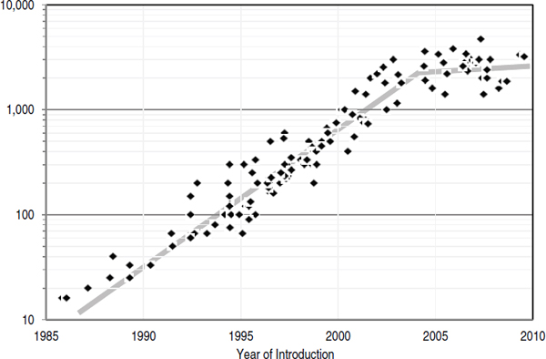
FIGURE 3.3 Microprocessor-clock frequency (MHz) over time (1985-2010).
expected performance. One might think that it should therefore be possible to continue to scale performance by doubling the number of processor cores. And, in fact, since the middle 1990s, some researchers have argued that chip multiprocessors (CMPs) can exploit capabilities of CMOS technology more effectively than single-processor chips.21 However, during the 1990s, the performance of single processors continued to scale at the rate of more than 50 percent per year, and power dissipation was still not a limiting factor, so those efforts did not receive wide attention. As single-processor performance scaling slowed down and the air-cooling power-dissipation limit became a major design constraint, researchers and industry shifted toward CMPs or multicore microprocessors.22
__________________________
21 Kunle Olukotun, Basem A. Nayfeh, Lance Hammond, Ken Wilson, and Kunyung Chang, 1996, The case for a single-chip multiprocessor, Proceedings of 7th International Conference on Architectural Support for Programming Languages and Operating Systems, Cambridge, Mass., October 1-5, 1996, pp. 2-11.
22 Listed here are some of the references that document, describe, and analyze this shift: Michael Bedford Taylor, Walter Lee, Jason Miller, David Wentzlaff, Ian Bratt, Ben Greenwald, Henry Hoffmann, Paul Johnson, Jason Kim, James Psota, Arvind Saraf, Nathan Shnidman, Volker Strumpen, Matt Frank, Saman Amarasinghe, and Anant Agarwal, 2004, Evaluation of the raw microprocessor: An exposed-wire-delay architecture for ILP and streams, Proceedings of the 31st Annual International Symposium on Computer Architecture, Munich,
The key observation motivating a CMP design is that to increase performance when the overall design is power-limited, each instruction needs to be executed with less energy. The power consumed is the energy per instruction times the performance (instructions per second). Examination of Intel microprocessor-design data from the i486 to the Pentium 4, for example, showed that power dissipation scales as performance raised to the 1.73 power after technology improvements are factored out. If the energy per instruction were constant, the relationship should be linear. Thus, the Intel Pentium 4 is about 6 times faster than the i486 in the same
Germany, June 19-23, 2004, pp. 2-13; Jung Ho Ahn, William J. Dally, Brucek Khailany, Ujval J. Kapasi, and Abhishek Das, 2004, Evaluating the imagine stream architecture, Proceedings of the 31st Annual International Symposium on Computer Architecture, Munich, Germany, June 19-23, 2004, pp. 14-25; Brucek Khailany, Ted Williams, Jim Lin, Eileen Peters Long, Mark Rygh, Deforest W. Tovey, and William Dally, 2008, A programmable 512 GOPS stream processor for signal, image, and video processing, IEEE Journal of Solid-State Circuits 43(1): 202-213; Christoforos Kozyrakis and David Patterson, 2002, Vector vs superscalar and VLIW architectures for embedded multimedia benchmarks, Proceedings of the 35th Annual ACM/IEEE International Symposium on Microarchitecture, Istanbul, Turkey, November 18-22, 2002, pp. 283-293; Luiz André Barroso, Kourosh Gharachorloo, Robert McNamara, Andreas Nowatzyk, Shaz Qadeer, Barton Sano, Scott Smith, Robert Stets, and Ben Verghese, 2000, Piranha: A scalable architecture based on single-chip multiprocessing, Proceedings of the 27th Annual International Symposium on Computer Architecture,Vancouver, British Columbia, Canada, June 10-14, 2000, pp. 282-293; Poonacha Kongetira, Kathirgamar Aingaran, and Kunle Olukotun, 2005, “Niagara: A 32-way multithreaded SPARC processor, IEEE Micro 25(2): 21-29; Dac C. Pham, Shigehiro Asano, Mark D. Bolliger, Michael N. Day, H. Peter Hofstee, Charles Johns, James A. Kahle, Atsushi Kameyama, John Keaty, Yoshio Masubuchi, Mack W. Riley, David Shippy, Daniel Stasiak, Masakazu Suzuoki, Michael F. Wang, James Warnock, Stephen Weitzel, Dieter F. Wendel, Takeshi Yamazaki, and Kazuaki Yazawa, 2005, The design and implementation of a first-generation CELL processor, IEEE International Solid-State Circuits Conference Digest of Technical Papers, San Francisco, Cal., February 10, 2005, pp. 184-185; R. Kalla, B. Sinharoy, and J.M. Tendler, 2004, IBM POWER5 chip: A dual-core multithreaded processor, IEEE Micro Magazine 24(2): 40-47; Toshinari Takayanagi, Jinuk Luke Shin, Bruce Petrick, Jeffrey Su, and Ana Sonia Leon, 2004, A dualcore 64b UltraSPARC microprocessor for dense server applications, IEEE International Solid-State Circuits Conference Digest of Technical Papers, San Francisco, Cal., February 15-19, 2004, pp. 58-59; Nabeel Sakran, Marcelo Uffe, Moty Mehelel, Jack Dowweck, Ernest Knoll, and Avi Kovacks, 2007, The implementation of the 65nm dual-core 64b Merom processor, IEEE International Solid-State Circuits Conference Digest of Technical Papers, San Francisco, Cal., February 11-15, 2007, pp. 106-107; Marc Tremblay and Shailender Chaudhry, 2008, A third-generation 65nm 16-core 32-thread plus 32-count-thread CMT SPARC processor, IEEE International Solid-State Circuits Conference Digest of Technical Papers, San Francisco, Cal., February 3-7, 2008, p. 82-83; Larry Seiler, Doug Carmean, Eric Sprangle, Tom Forsyth, Michael Abrash, Pradeep Dubey, Stephen Junkins, Adam Lake, Jeremy Sugerman, Robert Cavin, Roger Espasa, Ed Grochowski, Toni Juan, and Pat Hanrahan, 2008, “Larrabee: A many-core x86 architecture for visual computing, ACM Transactions on Graphics 27(3): 1-15; Doug Carmean, 2008, Larrabee: A many-core x86 architecture for visual computing, Hot Chips 20: A Symposium on High Performance Chips, Stanford, Cal., August 24-26, 2008.
technology but consumes 23 times more power23 and spends about 4 times more energy per instruction. That is another way of showing why single-processor power requirements increased because of circuit and architectural changes to improve performance. In achieving higher performance, the designs’ energy efficiency was worsening: performance scaled because of technology scaling and growing power budgets.
CMPs provide an alternative approach: using less aggressive processor-core design to reduce energy dissipation per instruction and at the same time using multiple-processor cores to scale overall chip performance. That approach allows one to use the growing number of transistors per chip to scale performance while staying within the limit of air-cooling. It increases chip parallelism, but only a specific type of coarse-grain program parallelism can exploit this type of parallelism.
Switching to chip multiprocessors reduces the effect of wire delays (the length of time it takes a signal—output from a gate—to travel along a given length of wire), which is growing relative to the gate delay (the length of time it takes to translate input to a logic gate to be transformed into output from that gate).24,25 Each processor in a CMP is small relative to the total chip area, and wires within a processor are short compared with the overall chip size. Interprocessor communication still requires long wires, but the latency of interprocessor communication is less critical for performance in a CMP system than is the latency between units within a single processor. In addition, the long wires can be pipelined and thus do not affect the clock-cycle time and performance of individual processors in a CMP.
Chip multiprocessors are a promising approach to scaling, but they face challenges as well; problems with modern scaling are described in the next section. Moreover, they cannot be programmed with the techniques that have proved successful for single processors; to achieve the potential performance of CMP, new software approaches and ultimately parallel applications must be developed. This will be discussed in the next chapter.
__________________________
23Ed Grochowski, Ronny Ronen, John Shen, and Hong Wang., 2004, Best of both latency and throughput, Proceedings of the IEEE International Conference on Computer Design, San Jose, Cal., October 11-13, 2004, pp. 236-243.
24Mark Horowitz and William Dally, 2004, How scaling will change processor architecture, IEEE International Solid States Circuits Conference Digest of Technical Papers, San Francisco, Cal., February 15-19, 2004, pp. 132-133
25Kunle Olukotun, Basem A. Nayfeh, Lance Hammond, Ken Wilson, and Kunyung Chang, 1996, The case for a single-chip multiprocessor, Proceedings of 7th International Conference on Architectural Support for Programming Languages and Operating Systems, Cambridge, Mass., October 1-5, 1996, pp. 2-11.
PROBLEMS IN SCALING NANOMETER DEVICES
If voltages could continue to be scaled with feature size (following classic Dennard scaling), CMP performance could continue to be scaled with technology. However, early in this decade scaling ran into some fundamental limits that make it impossible to continue along that path,26 and the improvements in both performance and power achieved with technology scaling have slowed from their historical rates. The net result is that even CMPs will run into power limitations. To understand those issues and their ramifications, we need to revisit technology scaling and look at one aspect of transistor performance that we ignored before: leakage current.
As described earlier, CMOS circuits have the important property that they dissipate energy only when a node changes value. Consider the simple but representative CMOS logic circuits in Figure 3.4. One type of CMOS device, a pMOS transistor, is connected to the power supply (Vsupply). When its input is low (Vgnd), it turns on, connects Vsupply to the output, and drives the output high to Vsupply. When the input to the pMOS device is high (Vsupply), it disconnects the output from Vsupply. The other type of CMOS device, an nMOS transistor, has the complementary behavior: when its input is high (Vsupply), it connects the output to Vgnd; when its input is low (Vgnd), it disconnects the output from Vgnd. Because of the construction of the CMOS logic, the pMOS and nMOS transistors are never driving the output at the same time. Hence, the only current that flows through the gate is that needed to charge or discharge the capacitances associated with the gate, so the energy consumed is mostly the energy needed to change the voltage on a capacitor with transistors, which is Cload multiplied by Vsupply2. For that analysis to hold, it is important that the off transistors not conduct any current in the off state: that is, they should have low leakage.
However, the voltage scaling that the industry has been following has indirectly been increasing leakage current. Transistors operate by changing the height of an energy barrier to modulate the number of carriers that can flow across them. One might expect a fairly sharp current transition, so that when the barrier is higher than the energy of the carriers, there is no current, and when it is lowered, the carriers can “spill” over and flow across the transistor. The actual situation is more complex. The basic reason is related to thermodynamics. At any finite temperature, although
__________________________
26Sam Naffziger reviews the Vdd limitations and describes various approaches (circuit, architecture, and so on) to future processor design given the voltage scaling limitations in the article High-performance processors in a power-limited world, Proceedings of the IEEE Symposium on VLSI Circuits, Honolulu, Hawaii, June 15-17, 2006, pp. 93-97, available online at http://ewh.ieee.org/r5/denver/sscs/Presentations/2006_11_Naffziger_paper.pdf.
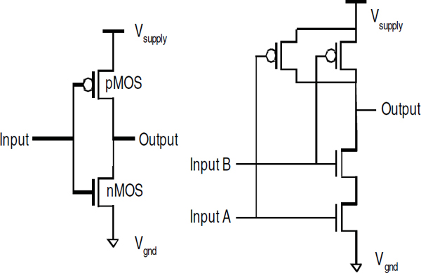
FIGURE 3.4 Representative CMOS logic circuits.
there is a well-defined average energy for the carriers, the energy of each individual carrier follows a probability distribution. The probability of having an energy higher than the average falls off exponentially, with a characteristic scale factor that is proportional to the temperature of the transistors measured measured in kelvins. The hotter the device, the wider the range of energies that the carriers can have.
That energy distribution is critical in the building of transistors. Even with an energy barrier that is higher than the average energy of the carriers, some carriers will flow over the barrier and through the transistor; the transistor will continue to conduct some current when we would like it to be off. The energy scale is kT, where k is the Boltzmann constant and T is the temperature in kelvins. We can convert it into voltage by dividing energy by the charge on the particle, an electron in this case: q = 1.6 × 10⁻¹⁹ coulombs. kT/q is around 26 mV at room temperature. Thus, the current through an off transistor drops exponentially with the height of the energy barrier, falling by slightly less than a factor of 3 for each 26-mV increase in the barrier height. The height of the barrier is normally called the threshold voltage (Vth) of the transistor, and the leakage current can be written as
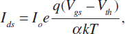
where Io is a constant around 1 μA (microampere) per micrometer of transistor width at room temperature, Vgs is the voltage applied to the control gate of the transistor, and α is a number greater than 1 (generally around 1.3) that represents how effectively the gate voltage changes the energy barrier. From the equation, it is easy to see that the amount of leakage current through an off transistor (Vgs = 0) depends heavily on the transistor’s threshold voltage. The leakage current increases by about a factor of 10 each time the threshold voltage drops by another 100 mV.
Historically, Vths were around 800 mV, so the residual transistor leakage currents were so small that they did not matter. Starting from high Vth values, it was possible to scale Vth, Vsupply, and L together. While leakage current grew exponentially with shrinking Vth, the contribution of subthreshold leakage to the overall power was negligible as long as Vth values were still relatively large. But ultimately by the 90-nm node, the leakage grew to a point where it started to affect overall chip power.27 At that point, Vth and Vsupply scaling slowed dramatically.
One approach to reduce leakage current is to reduce temperature, inasmuch as this makes the exponential slope steeper. That is possible and has been tried on occasion, but it runs into two problems. The first is that one needs to consider the power and cost of providing a low-temperature environment, which usually dwarf the gains provided by the system; this is especially true for small or middle-size systems that operate in an office or home environment. The second is related to testing, repair, thermal cycling, and reliability of the systems. For those reasons, we will not consider this option further in the present report. However, for sufficiently large computing centers, it may prove advantageous to use liquid cooling or other chilling approaches where the energy costs of operating the semiconductor hardware in a low-temperature environment do not outweigh the performance gains, and hence energy savings, that are possible in such an environment.
Vth stopped scaling because of increasing leakage currents, and Vsupply scaling slowed to preserve transistor speed with a constant (Vsupply – Vth). Once leakage becomes important, an interesting optimization between Vsupply and Vth is possible. Increasing Vth decreases leakage current but also makes the gates slower because the number of carriers that can flow through a transistor is roughly proportional to the decreasing (Vsupply – Vth). One can recover the lost speed by increasing Vsupply, but this also increases the power consumed to switch the gate dynamically. For a given gate delay, the lowest-power solution is one in which the marginal energy cost of increasing Vdd is exactly balanced by the marginal energy savings
__________________________
27Edward J. Nowak, 2002, Maintaining the benefits of CMOS scaling when scaling bogs down, IBM Journal of Research and Development 46(2/3): 169-180.
of increasing Vth. The balance occurs when the static leakage power is roughly 30 percent of the dynamic power dissipation.
This leakage-constrained scaling began at roughly the 130-nm technology node, and today both Vsupply and Vth scaling have dramatically slowed; this has also changed how gate energy and speed scale with technology. The energy required to switch a gate is C multiplied by Vsupply2, which scales only as 1/κ if Vsupply is not scaling. That means that technology scaling reduces the power by κ only if the scaled circuit is run at the same frequency. That is, if gate speed continued to increase, half the die (the size of the scaled circuit) would dissipate the same power as the full die in the previous generation and would operate κ times, that is 1.4 times, faster, much less than the three-fold performance increase we have come to expect. Clearly, that is not optimal, so many designers are scaling Vdd slightly to increase the energy savings. That works but lowers the gate speeds, so some parallelism is needed just to recover from the slowing single-thread performance. The poor scaling will eventually limit the performance of CMPs.
Combining the lessons of the last several sections of this chapter, the committee concluded that neither CMOS nor chip multiprocessors can overcome the power limits facing modern computer systems. That leads to another core conclusion of this report. Basic laws of physics and constraints on chip design mean that the growth in the performance of computer systems will become limited by their power and thermal requirements within the next decade. Optimists might hope that new technologies and new research could overcome that limitation and allow hardware to continue to drive future performance scaling akin to what we have seen with single-thread performance, but there are reasons for caution, as described in the next section.
Finding: The growth in the performance of computing systems—even if they are multiple-processor parallel systems—will become limited by power consumption within a decade.
ADVANCED TECHNOLOGY OPTIONS
If CMOS scaling, even in chip-multiprocessor designs, is reaching limits, it is natural to ask whether other technology options might get around the limits and eventually overtake CMOS, as CMOS did to nMOS and bipolar circuits in the 1980s. The answer to the question is mixed.28 It
__________________________
28 Mark Bohr, Intel senior fellow, gave a plenary talk at ISSCC 2009 on scaling in an SOC world in which he argues that “our challenge … is to recognize the coming revolutionary
is clear that new technologies and techniques will be created and applied to scaled technologies, but these major advances—such as high-k gate dielectrics, low-K interconnect dielectrics, and strained silicon—will probably be used to continue technology scaling in general and not create a disruptive change in the technology. Recent press reports make it clear, for example, that Intel expects to be using silicon supplemented with other materials in future generations of chips.29
A recent study compared estimated gate speed and energy of transistors built with exotic materials that should have very high performance.30 Although the results were positive, the maximum improvement at the same power was modest, around a factor of 2 for the best technology. Those results should not be surprising. The fundamental problem is that Vth does not scale, so it is hard to scale the supply voltage. The limitation on Vth is set by leakage of carriers over an energy barrier, so any device that modulates current by changing an energy barrier should have similar limitations. All the devices used in the study cited above used the same current-control method, as do transistors made from nanotubes, nanowires, graphene, and so on. To get around that limitation, one needs to change “the game” and build devices that work by different principles. A few options are being pursued, but each has serious issues that would need to be overcome before they could become practical.
One alternative approach is to stop using an energy barrier to control current flow and instead use quantum mechanical tunneling. That approach eliminates the problem with the energy tails by using carriers that are constrained by the energy bands in the silicon, which have fixed levels. Because there is no energy tail, they can have, in theory, a steep turnon characteristic. Many researchers are trying to create a useful device of this type, but there are a number of challenges. The first is to create a large enough current ratio in a small enough voltage range. The tunneling current will turn on rapidly, but its increase with voltage is not that rapid. Because a current ratio of around 10,000 is required, we need a device that can transition through this current range in a small voltage (<400 mV).
__________________________
changes and opportunities and to prepare to utilize them (Mark Bohr, 2009, The new era of scaling in an SOC world, IEEE International Solid-State Circuits Conference, San Francisco, Cal., February 9, 2009, available online at http://download.intel.com/technology/architecture-silicon/ISSCC_09_plenary_paper_Bohr.pdf).
29 Intel CEO Paul Ottelini was said to have declared that silicon was in its last decade as the base material of the CPU (David Flynn, 2009, Intel looks beyond silicon for processors past 2017, Apcmag.com, October 29, 2009, available online at http://apcmag.com/intel-looksbeyond-silicon-for-processors-past-2017.htm).
30 Donghyun Kim, Tejas Krishnamohan1, and Krishna C. Saraswat, 2008, Performance evaluation of 15nm gate length double-gate n-MOSFETs with high mobility channels: III-V, Ge and Si, Electrochemical Society Transactions 16(11): 47-55.
Even if one can create a device with that current ratio, another problem arises. The speed of the gates depends on the transistor current. So not only do we need the current ratio, we also need devices that can supply roughly the same magnitude of current as CMOS transistors provide. Tunnel currents are often small, so best estimates indicate that tunnel FETs might be much slower (less current) than in CMOS transistors. Such slowness will make their adoption difficult.
Another group of researchers are trying to leverage the collective effort of many particles together to get around the voltage limits of CMOS. Recall that the operating voltage is set by the thermal energy (kT) divided by the charge on one electron, because that is the charged particle. If the charged particle had a charge of 2q, the voltage requirements would be half what it is today. That is the approach that nerve cells use to operate robustly at low voltages. The proteins in the voltage-activated ion channels have a charge that allows them to operate easily at 100 mV. Although some groups have been trying to create paired charge carriers, most are looking at other types of cooperative processes. The ion channels in nerves go though a physical change, so many groups are trying to build logic from nanorelays (nanomicroelectromechanical systems, or nano MEMS). Because of the large number of charges on the gate electrode and the positive feedback intrinsic in electrostatic devices, it is theoretically possible to have very low operating voltages; indeed, operation down to a couple of tenths of a volt seems possible. Even as researchers work to overcome that hurdle, there are a number of issues that need to be addressed. The most important is determining the minimum operating voltage that can reliably overcome contact sticking. It might not take much voltage to create a contact, but if the two surfaces that connect stick together (either because of molecular forces or because of microwelding from the current flow), larger voltages will be needed to break the contact. Devices will have large numbers of these structures, so the voltage must be less than CMOS operating voltages at similar performance. The second issue is performance and reliability. This device depends on a mechanically moving structure, so the delay will probably be larger than that of CMOS (around 1 nanosecond), and it will probably be an additional challenge to build structures that can move for billions of cycles without failing.
There is also promising research in the use of electron-spin-based devices (spintronics) in contrast with the charge-based devices (electronics) in use today. Spin-based devices—and even pseudospin devices, such as the BiSFET31—have the potential to greatly reduce the power dissi-
__________________________
31 Sanjay K.Banerjee, Leonard F. Register, Emanuel Tutuc, Dharmendar Reddy, and Allan H. MacDonald, 2009, Bilayer pseudospin field-effect transistor (BiSFET): A proposed new logic device, IEEE Electron Device Letters30(2): 158-160.
pated in performing basic logic functions. However, large fundamental and practical problems remain to be solved before spintronic systems can become practical.32 Those or other approaches (such as using the correlation of particles in ferro materials33) might yield a breakthrough. However, given the complexity of today’s chips, with billions of working transistors, it is likely to take at least a decade to introduce any new technology into volume manufacturing. Thus, although we should continue to invest in technology research, we cannot count on it to save the day. It is unlikely to change the situation in the next decade.
Recommendation: Invest in research and development to make computer systems more power-efficient at all levels of the system, including software, application-specific approaches, and alternative devices. R&D should be aimed at making logic gates more power-efficient. Such efforts should address alternative physical devices beyond incremental improvements in today’s CMOS circuits.
APPLICATION-SPECIFIC INTEGRATED CIRCUITS
Although the shift toward chip multiprocessors will allow industry to continue to scale the performance of CMPs based on general-purpose processor cores for some time, general-purpose chip multiprocessors will reach their own limit. As discussed earlier, CMP designers can trade off single-thread performance of individual processors against lower energy dissipation per instruction, thus allowing more instructions by multiple processors while the same amount of energy is dissipated by the chip. However, that is possible only within some range of energy performance. Beyond some limit, lowering energy per instruction by processor simplification can lead to overall CMP performance degradation because processor performance starts to decrease faster than energy per instruction. That range is likely to be a factor of about 10, that is, energy per instruction cannot be reduced by more than a factor of 10 compared with the highest-performance single-processor chip, such as the Intel Pentium 4 or the Intel Itanium.34
When such limits are reached, we will need to create other approaches
__________________________
32 In their article, cited in the preceding footnote, Banerjee et al. look at a promising technology that still faces many challenges.
33 See, for instance, the research of Sayeef Salahuddin at the University of California, Berkeley.
34 The real gain might be even smaller because with an increase in the number of processors on the chip, more energy will be dissipated by the memory system and interconnect, or the performance of many parallel applications will scale less than linearly with the number of processors.
to create an energy-efficient computation unit. On the basis of the historical data, the answer seems clear: we will need to create more application-optimized processing units. It is well known that tuning the hardware and software toward a specific application or set of applications allows a more energy-efficient solution. That work started with the digital watch many decades ago and continues today. Figure 3.5 shows data for general-purpose processors, digital-signal processors, and application-specific integrated circuits (ASICs) from publications presented at the International Solid-State Circuits Conference. The data are somewhat dated, but all chips were designed for similar 0.18- to 0.25-μm CMOS technology, and one can see that the ASIC designs are roughly 3 orders of magnitude more energy-efficient than the general-purpose processors.
The main reason for such a difference is a combination of algorithm and hardware tuning and the ability to reduce the use of large memory structures as general interconnects: instead of a value’s being stored in a register or memory, it is consumed by the next function unit. Doing only what needs to be done saves both energy and area (see Figure 3.6).
More recently, researchers at Lawrence Berkeley National Laboratory, interested in building peta-scale supercomputers for kilometer-scale climate modeling, argued that designing a specialized supercomputer based on highly efficient customizable embedded processors can be attractive in terms of energy cost.35 For example, they estimated that a peta-scale climate supercomputer built with custom chips would consume 2.5 MW of electric power whereas a computer with the same level of performance but built with general-purpose AMD processors would require 179 MW.
The current design trend, however, is away from building customized solutions; increasing design complexity has caused the nonrecurring engineering costs for designing these chips to grow rapidly. Typical ASIC design requires $20-50 million, which limits the range of market segments to very few with volumes high enough to justify the initial engineering investment. Thus, if we do need to create more application-optimized computing systems, we will need to create a new approach to design that will allow a small team to create an application-specific chip at reasonable cost. That leads to this chapter’s overarching recommendation. Efforts are needed along multiple paths to deal with the power limitations that modern scaling and computer-chip designs are encountering.
__________________________
35 Michael Wehner, Leonid Oliker, and John Shalf, 2008, Towards ultra-high resolution models of climate and weather, International Journal of High Performance Computing Applications 22(2): 149-165.
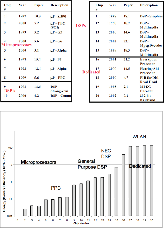
FIGURE 3.5 Energy efficiency comparison of CPUs, DSPs, and ASICs. SOURCE: Robert Brodersen of the University of California, Berkeley, and Teresa Meng of Stanford University. Data published at International Solid-State Circuits Conference (0.18- to 0.25-μm).
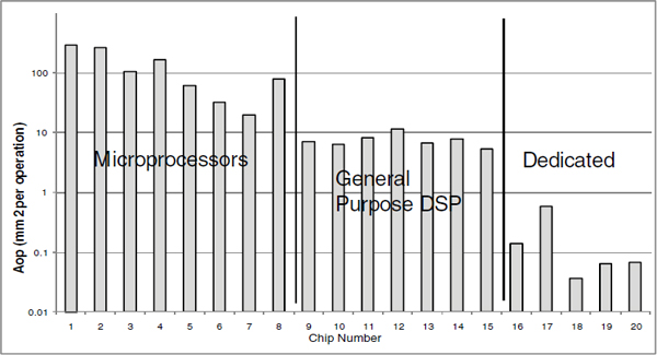
FIGURE 3.6 Area efficiency comparison of CPUs, DSPs, and ASICs. SOURCE: Robert Brodersen of the University of California at Berkeley and Teresa Meng of Stanford University.
Recommendation: Invest in research and development of parallel architectures driven by applications, including enhancements of chip multiprocessor systems and conventional data-parallel architectures, cost-effective designs for application-specific architectures, and support for radically different approaches.
BIBLIOGRAPHY
Broderson, Robert. “Interview: A Conversation with Teresa Meng.” ACM Queue 2(6): 14-21, 2004.
Chabini, Noureddine, Ismaïl Chabini, El Mostapha Aboulhamid, and Yvon Savaria. “Methods for Minimizing Dynamic Power Consumption in Synchronous Designs with Multiple Supply Voltages.” In IEEE Transactions on Computer-Aided Design of Integrated Circuits and Systems 22(3): 346-351, 2003.
Copeland, Jack. Colossus: The Secrets of Bletchley Park’s Code-Breaking Computers. New York: Oxford University Press, 2006.
International Technology Roadmap for Semiconductors (ITRS). “System Drivers.” ITRS 2007 Edition. Available online at http://www.itrs.net/Links/2007ITRS/Home2007.htm.
Kannan, Hari, Fei Guo, Li Zhao, Ramesh Illikkal, Ravi Iyer, Don Newell, Yan Solihin, and Christos Kozyrakis. “From Chaos to QoS: Case Studies in CMP Resource Manage-ment.” At the 2nd Workshop on Design, Architecture, and Simulation of Chip-Multiprocessors (dasCMP). Orlando, Fla., December 10, 2006.
Khailany, Brucek, William J. Dally, Scott Rixner, Ujval J. Kapasi, Peter Mattson, Jinyung Namkoong, John D. Owens, Brian Towles, and Andrew Chang. “Imagine: Media Processing with Streams.” IEEE Micro 21(2): 35-46, 2001.
Knight, Tom. 1986.“An Architecture for Mostly Functional Languages.” In Proceedings of ACM Conference on LISP and Functional Programming. Cambridge, Mass., August 4-6, 1986, pp. 105-112.
Poonacha Kongetira, Kathirgamar Aingaran, and Kunle Olukotun. “Niagara: A 32-way Multithreaded Sparc Processor.” IEEE Micro 25(2):21-29 2005, 2005.
Lee, Edward A. “The Problem with Threads.” IEEE Computer 39(5): 33-42, 2006.
Lee, Walter, Rajeev Barua, Matthew Frank, Devabhaktuni Srikrishna, Jonathan Babb, Vivek Sarkar, and Saman Amarasinghe. “Space-time Scheduling of Instruction-level Parallelism on a Raw Machine.” In Proceedings of the Eighth International Conference on Architectural Support for Programming Language and Operating Systems. San Jose, Cal., October 3-7, 1998, pp. 46-57.
Lomet, David B., “Process Structuring, Synchronization, and Recovery Using Atomic Actions,” In Proceedings of the ACM Conference on Language Design for Reliable Software. Raleigh, N.C., March 28-30, 1977, pp. 128-137.
Marković, Dejan, Borivoje Nikolić, and Robert W. Brodersen. “Power and Area Minimization for Multidimensional Signal Processing.” IEEE Journal of Solid-State Circuits 42(4): 922-934, 2007.
Nowak, Edward J. “Maintaining the Benefits of CMOS Scaling When Scaling Bogs Down.” IBM Journal of Research and Development 46(2/3):169-180, 2002.
Rixner, Scott, William J. Dally, Ujval J. Kapasi, Brucek Khailany, Abelardo López-Lagunas, Peter R. Mattson, and John D. Owens. “A Bandwidth-Efficient Architecture for Media Processing.” In Proceedings of the International Symposium on Microarchitecture. Dallas, Tex.: November 30-December 2, 1998, pp. 3-13, 1998.
Rusu, Stefan, Simon Tam, Harry Muljono, David Ayers, and Jonathan Chang. “A Dual-core Multi-threaded Xeon Processor with 16MB L3 Cache.” In IEEE International Solid-State Circuits Conference Digest of Technical Papers. San Francisco, Cal., February 6-9, 2006, pp. 315-324.
Sandararajan, Vijay, and Keshab Parhi. “Synthesis of Low Power CMOS VLSI Circuits Using Dual Supply Voltages.” In Proceedings of the 35th Design Automation Conference. New Orleans, La.., June 21-25, 1999, pp. 72-75.
Sutter, Herb, and James Larus. “Software and the Concurrency Revolution.” ACM Queue 3(7): 54-62, 2005.
Taur, Yuan, and Tak H. Ning, Fundamentals of Modern VLSI Devices, Ninth Edition, New York: Cambridge University Press, 2006.
Thies, Bill, Michal Karczmarek, and Saman Amarasinghe. “StreamIt: A Language for Streaming Applications.” In Proceedings of the International Conference on Compiler Construction. Grenoble, France, April 8-12, 2002, pp. 179-196.
Wehner, Michael, Leonid Oliker, and John Shalf. “Towards Ultra-High Resolution Models of Climate and Weather.” International Journal of High Performance Computing Application 22(2): 149-165, 2008.
Zhao, Li, Ravi Iyer, Ramesh Illikkal, Jaideep Moses, Srihari Makineni, and Don Newell. “CacheScouts: Fine-Grain Monitoring of Shared Caches in CMP Platforms.” In Proceedings of the 16th International Conference on Parallel Architecture and Compilation Techniques. Brasov, Romania, September 15-19, 2007, pp. 339-352.


