
3
Semiconductors
The lessons learned from the committee's examination of factory site selection in the semiconductor industry are similar to those from the telephone and television analyses. With the exception of high-volume, labor-intense assembly operations, which historically have been located in Asia to minimize labor costs, site selection in the semiconductor industry depends more on factors such as market access and skilled labor availability than on input costs. Although rigorous data on semiconductor production costs were not available to the committee, its discussions with many U.S. semiconductor firms support this conclusion.
The committee's analysis of semiconductors is complicated by the heterogeneity of the industry. Factors that determine production costs vary substantially across device types and technologies. For leading-edge products, such as advanced dynamic random access memories (DRAMs) and microprocessors, manufacturing is capital intense, with R&D and equipment investment requirements rising steadily. Manufacturing competitiveness depends on managing the production process to achieve high-capacity utilization, high yields, and timely market entry and to assure broad market access to achieve high production volumes. For less advanced products, such as microcontrollers, application-specific integrated circuits (ASICs), and analog devices, costs are driven more by packaging and
testing because the process technology is older, less advanced, and less expensive. Because of this diversity in the industry, the factors that make specific locations attractive vary widely depending on the specific product and stage of production.
A further complication in trying to understand site selection decisions in the industry is the prevalence of trade barriers. Barriers take a variety of forms but typically are based on local content requirements (prevalent in Europe and many developing countries), minimum prices to counter dumping, and market share constraints/goals.1 The result is that major producers have fabrication facilities all over the world, new investments are strategically located to ensure access to crucial markets, and increasing interterm collaboration is partially motivated by the need for assured markets and sources of supply.
The combination of these factors means that factory location for advanced products is an integral part of gaining market access to allow sufficient production volumes to amortize high fixed costs from R&D and capital equipment requirements. For low-end products, site selection may be based more on where customers are located to maximize market responsiveness. Almost regardless of the product, packaging tends to be labor-intensive and most is done in Asia.
BACKGROUND
The semiconductor industry represents a significant and growing segment of U.S. manufacturing, as well as a vital link in the global production chain for electronics products. Within the United States, the semiconductor industry is presently one of the fastest growing (in constant dollar shipments) of any four-digit SIC code industry, at 7.9 percent annual growth in 1991.2 Taken by itself, the world semiconductor market was worth about $54.6 billion in 1991.3 As the basis for a wide variety of electronics products, semiconductors are strategically linked to a global electronics market worth $750 billion. The semiconductor market is itself, in turn, supported by a semiconductor equipment and materials market worth $20 billion.4
Though typically discussed in general terms, the semiconductor market is divided into several distinct product segments. By volume, the largest segment is memory devices, such as
dynamic random access memories and static random access memories (SRAMs). This segment has come to be dominated by Japanese producers. Logic devices are the second-largest segment, with American suppliers (mainly Intel and Motorola) dominating the medium and high ends of the business (microprocessors)5 and Japanese firms leading in the lower end (microcontrollers).6 ASICs are custom devices; both U.S. and Japanese suppliers have strong positions in this segment.
Concern about the competitiveness of the U.S. semiconductor industry has been driven almost exclusively by losses in the DRAM market, which have been mirrored by Japanese gains (Figure 3-1).7 The loss of American DRAM production, in turn, has been held responsible for losses in market share in production equipment and materials. As the volume leader and manufacturing process driver (feature density has increased faster in DRAMs and led developments in other product segments), DRAM production demands increases in process equipment accuracy and throughput, as well as material purity. Such realizations have spurred several U.S. manufacturers to take steps to reenter the DRAM market, typically through joint ventures with Japanese producers.8
Several explanations for U.S. market share losses have been offered, many of which suggest that the Japanese manufactur-
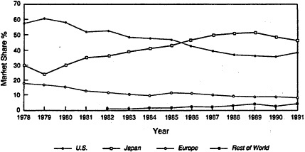
Figure 3-1
World production of semiconductors by region.
Sources: National Advisory Committee on Semiconductors Report 1991 and Dataquest.
ing environment is one that gives Japanese firms unique cost advantages. The premise behind this explanation—that a firm's location helps determine both its costs and, ultimately, its competitive success—is precisely the sort of assumption that this committee was formed to examine.
Industry Structure
Perhaps the primary factor identified as providing Japanese firms with a distinct advantage is the difference in industry structure in the two countries. The Japanese market is an oligopoly in which semiconductor production is dominated by a few large, diversified, vertically integrated firms (e.g., NEC, Fujitsu, Hitachi, Toshiba, Mitsubishi, Sony, and Matsushita). In each of these firms, semiconductor sales account for 10 to 25 percent of total revenues. Nearly one-fourth of the semiconductors produced by each firm are used in its own products. These products range from computers to communications equipment to consumer electronics.9 Often, these firms hold equity positions in other diversified firms that supply capital equipment, materials, and services. These relationships knit together common interests, the end result being a Japanese semiconductor market that is both highly responsive to product requirements and highly integrated throughout the supply/production chain.
Historically, the American semiconductor industry has had two segments: captive—internal production for internal use, and merchant—production for sale on the open market. This distinction has blurred somewhat in recent years and is expected to diminish significantly through the 1990s. The main captive manufacturers have been IBM, AT&T, and General Motors (Delco). However, fully 50 percent of AT&T's semiconductor production is now sold in the open market, and IBM is projected to be the leading merchant producer by 1995. Although there are a few major exceptions (Intel, Motorola, Texas Instruments), merchant producers tend to be relatively small, relying on semiconductor sales for the majority of their revenues. Many of these firms were founded by individuals who broke from major corporations to start their own operations. Within this segment of the U.S. industry, there are few
stable relationships with suppliers. The Supplier base, too, is fragmented.10
There has been a large influx of Japanese investment in semiconductor manufacturing in the United States since the U.S.-Japan semiconductor trade agreement in 1986. However, only 21 percent of the employment resulting from that investment came from new investments, with 79 percent of employment coming from acquired plants.11 Most of this investment has been purchases of U.S. equipment and materials suppliers, though a growing number of fabrication facilities have been established, both to assure market access and to exploit exchange rate differentials.
IMPORTANCE OF PROCESS CONTROL
Semiconductor fabrication is fundamentally capital intensive, though capital requirements vary somewhat by device type, with leading-edge products requiring large and growing investment. For instance, the cost of a new microprocessor fabrication facility (fab) is about $500 million; a 4-megabit DRAM fab costs about $350 million. These estimates are just for the facilities and do not include related preproduction R&D and design costs. Future generations of devices are estimated to cost significantly more. A facility capable of mass producing 64-megabit DRAMs is expected to cost $750 million, in addition to development costs of between $600 million and $1 billion.12
Such escalating expenses are driving an increasing number of corporate alliances in the industry designed to share costs, speed development, and broaden market access to assure needed production volumes. Texas Instruments and Hitachi, Motorola and Toshiba, AT&T and NEC, and IBM and Siemens have all announced cooperative agreements to develop the technologies necessary to shrink chip geometries to less than half a micron, required for the next-generations of DRAMs.13 SEMATECH, an industry consortium including both semiconductor manufacturers and equipment producers and partially funded by the federal government, is another example of cooperation intended to spread R&D costs, share information, and hasten technology development and implementation.
The high capital requirements for DRAM production help to explain the rapid increases in Japanese market share. Throughout the late 1980s the major Japanese producers greatly outspent the top American merchant producers in both R&D and capital equipment investment. In 1989 alone the Japanese spent over $1 billion more in R&D and over $2 billion more in capital equipment.14
The reasons for this differential are complex. Some analysts attribute it to lower capital costs in Japan, though there is no consensus on that point. Another factor is industry structure. Because Japanese producers are large, vertically integrated corporations and are part of large keiretsus, they tend to be better financed than American merchant producers and have the flexibility to use the profits generated by other businesses to fund semiconductor investment. Faster capital depreciation rates also allow more aggressive investment strategies. For tax purposes, Japanese firms use a three-year accelerated depreciation schedule (54 percent in year one, 30 percent in year two, and 16 percent in year three); in the United States, current depreciation schedules for semiconductor manufacturing equipment permit tax depreciation over five years, although some equipment is depreciated over three to four years for financial reporting.15
Given this capital intensity, the determinants of product cost largely flow from changes in manufacturing process parameters, such as capacity utilization, yields, and production volume. Some insight into the relative impact of changes in various manufacturing process parameters on production costs can be gained using computer modeling. A 1989 study done for the Semiconductor Research Corporation modeled the production processes required to make a 256k CMOS SRAM.16 The model was designed to indicate the required selling price for the chip, given profitability objectives, as parameters in the manufacturing process are changed. Thus, it is useful both in highlighting many of the process variables critical to effective chip production and in illustrating the effects of changes on manufacturing costs.
Figure 3-2 illustrates the results of the model for a number of parameters. The number of chips per wafer has the greatest impact on production costs, though the model assumes chips
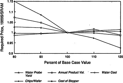
Figure 3-2
Sensitivity of required SRAM price to selected parameters.
Source: Semiconductor Research Corp. (1989).
per wafer to be a function of product design, not changes in wafer size. (Larger wafers hold more chips, but changing wafer size requires changing much of the process equipment.17) Production volume also has a large impact on costs, with the model simulating volumes ranging from 24 million to 36 million chips per year. Control of the manufacturing process as reflected in yields also has a significant impact on costs. Several other variables with lesser effects are also illustrated. Though useful in illustrating several cost drivers, the model does not address others, and by focusing on one product it is not truly indicative of the production challenges facing semiconductor manufacturers.
Processing requirements for different types of devices vary tremendously, affecting the complexity of the plant, the number of processing steps, and the flow of materials. Despite the difficulties of achieving submicron dimensions, DRAM fabrication is much less complicated than that for microprocessors and ASICs. Because DRAM designs tend to be repetitive arrays, a DRAM plant typically produces one design with minor
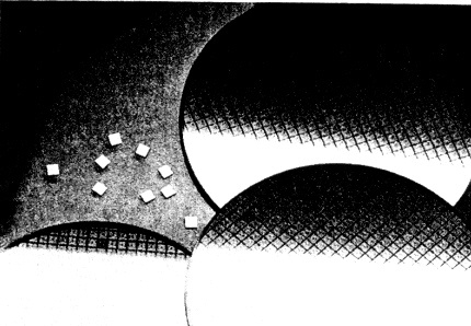
Close-up of silicon wafer and individual chips after processing.
Source: National Semiconductor.
variations, thereby reducing the number of changes necessary in the process and allowing greater scale economies. In contrast, because a microprocessor typically contains both memory and logic devices on the same chip, design complexity is much greater. As a result, microprocessor factories may produce 20 to 30 major design variations at one time. Compared to DRAMs, batch sizes are smaller and material flow is much more complex; while the nature of the individual processing steps is the same, microprocessors require significantly more steps than DRAMs. ASICs represent a still different set of control challenges. An ASIC plant may be producing hundreds of designs, so managing wafer flow and device testing are critical for cost-effective production.
Controlling such complex manufacturing systems to maximize equipment utilization and yields, in a hazardous environment with extraordinary standards for cleanliness and precision, is a daunting management task. Japanese competitors have proven adept at minimizing variability in the process to
achieve high yields, and several U.S. producers, most notably Motorola and Intel, have made impressive progress in matching Japanese accomplishments. Using many of the precepts of total quality management—design for manufacturability, preventive maintenance, close relations with equipment and materials suppliers, broad-based training of a skilled work force, etc.—firms are able to achieve higher yields when a new line is opened and to improve yields rapidly.
Labor Costs
Given the sophisticated equipment involved and the importance of maximizing output from that equipment, it is to be expected that skilled workers comprise the greatest proportion of labor costs in wafer fabrication. According to data supplied by Digital Equipment Corporation, skilled labor accounts for 35 percent of production costs for microprocessor and custom device fabrication (Table 3-1). As such, the availability of the skills required is a significant constraint on site selection.
After the fabrication stage, packaging and testing are the final steps in producing a finished chip. Because individual chips are being assembled into packaged semiconductors—instead of entire wafers being processed—this part of the manu-
TABLE 3-1
Production Cost Structure for Wafer Fabrication Microprocessor and Custom Devices
|
Material |
15% |
|
Depreciation |
15 |
|
Labor costs |
|
|
Semiskilled |
4 |
|
Administrative (managers, secretaries, etc.) |
7 |
|
Skilled and highly skilled technical |
35 |
|
Other costs, occupancy, utilities, etc. |
24 |
|
|
100% |
|
SOURCE: Digital Equipment Corporation (1991). |
|
facturing process has relied on unskilled and semiskilled labor. In fact, as device technology matures and less sophisticated products are considered, the costs of packaging and testing grow as a proportion of total costs. Most semiconductor assembly has been located in newly industrialized, low wage countries in Asia. Malaysia, in particular, has been very successful in attracting semiconductor assembly operations. The source of its popularity has changed over time, however. Ten years ago Malaysia's attraction was low-cost labor; today the presence of a large number of packaging operations has created a critical mass of talent, experience, and suppliers, making Malaysia an important source of packaging innovations.
Several developments in packaging and testing may change the cost structure of both of these activities. Built-in self-test, a means of testing a chip while it is still on an uncut wafer, should make testing more easily automated. Manufacturers are also beginning to place more than one chip in a single package to create multichip modules. Because of the performance advantages they provide, multichip modules are expected to capture an increasing share of semiconductor packaging; the still-emerging technology is likely to change the economics and technological expertise needed for packaging, which could eliminate the importance of offshore cost advantages.
LOCATION DECISIONS
Since U.S. firms began siting wafer fabs abroad in the 1970s and 1980s, the need to achieve high-capacity utilization and rapid time to market have driven site selections based on proximity to customers, market access, and the ability to operate manufacturing and process technologies to achieve high quality and high yields. Low-cost labor is not a consideration, but high-quality, highly skilled labor availability is.
Recent location decisions taken by U.S.-owned firms illustrate these changes. For example, Digital recently located a microprocessor fabrication facility in South Queensferry, Scotland. The reported criteria for selection were, in order of priority:
-
availability of skilled people
-
infrastructure (power, waste treatment, etc.)
-
market access to the European Economic Community
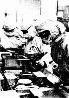
Workers monitor the manufacturing process in the clean room of a silicon wafer fabrication facility in Arlington, Texas.
Source: National Semiconductor.
-
government grants
-
operating costs
Other factors falling lower in importance were access to design engineers (those designing circuits for end customers), equipment availability, and access to capital. This last item did not weigh heavily in the decision because Digital has access to capital worldwide.
The fourth item on the list—government grants—has become a controversial factor in site selection decisions; however, as with the Digital illustration, government incentives are not typically the determining factor. A potential site must first have all the major prerequisites—killed work force, infrastructure, and market access—before government incentives can play a determining factor. In Digital's case, South Queensferry is in an area known as “Silicon Glen” where a growing number of semiconductor facilities are also located, not only ensuring skill and infrastructure availability but also providing a track record for Digital's management to consider. As an additional incen-
tive, Scotland offered grants for capital, training, and employment that accounted for an estimated 15 percent of the initial investment in the facility.18
This example illustrates two important points. First, government incentives can make a significant difference to a prospective manufacturer, but only when it must choose from a variety of locations that are otherwise similar with respect to market access and access to skilled workers and technologies. Second, although there are certain site characteristics that are essential, other factors, often subtle and unique to particular managers, can be major determinants.
In the 1990s the United States may be viewed more and more favorably as a location for both wafer fabrication and packaging, although many of the sources of technology, processes, and equipment may be Japanese. The drivers are a combination of technology shifts and trade policies. Already several Japanese firms have set up fabrication facilities in the United States, both to gain access to U.S. markets in the face of protectionist trade policies and to exploit exchange rate differentials. As stated above, Japanese firms have also bought existing U.S. firms (most conspicuously those in the semiconductor materials and equipment sector). While such investments might not constitute a site location abroad, per se, the acquisition of foreign capacity represents a de facto decision to move capacity offshore.
CONCLUSIONS
From its examination of the semiconductor industry, the committee offers the following conclusions about cost, site location, and competitiveness.
-
Firms must make huge capital investments to be players in the market, but success is secured by maximizing the returns on that investment, not by whittling down the initial outlay. The large capital expenditure makes capital efficiency (short cycle time, high throughput, yield improvements, and quality) all the more critical. If these are anything short of exceptional, a firm may lose a major share of the initial investment, market share, or even the business itself. Market access
-
and access to technologies and capabilities will continue to be the overriding concerns in site location decisions.
-
Regardless of how efficient a manufacturer is, unfair trade practices, such as product dumping, can have catastrophic effects when firms find themselves unable to recoup huge capital investments because a competitor is selling far below production costs.
-
The semiconductor industry will continue its tendency toward research consortia and joint ventures, motivated by high R&D and capital costs and the need for secure supplier relations and market access. When firms team up to develop and manufacture new device generations, they have the opportunity to learn better ways of manufacturing and of sharing investment risk. The predominance of foreign firms as the preferred partner in joint ventures, however, raises some interesting questions. Is this due to the fact that only foreign firms have the complementary skills and knowledge sought by American manufacturers? Or are government policies, particularly trade policies and local content requirements, driving these decisions?
-
Countries are trading market access for semiconductor manufacturing technology.
-
Being a successful semiconductor manufacturer means knowing how to manage capital effectively. Domestic manufacturers are at a distinct disadvantage in this respect when either stockholder expectations or depreciation schedules force them to manage capital suboptimally.
-
As market access and access to technologies/capabilities continue to determine where semiconductor manufacturers locate their facilities, the United States will be a viable place to make semiconductors in the future. The United States will be excluded as a potential manufacturing location, however, if
-
it cannot provide engineers and skilled technicians in sufficient numbers,
-
the skill base for advanced manufacturing (both in managerial and technical terms) continues to erode as Americans lose market share and thus experience with technology/process-driving devices, or
-
customers for semiconductors—electronics firms—leave the United States in sufficient numbers that manufacturers prefer to follow them abroad.


