
7
Modeling of Optically "Assisted" Phased Array Radar
Alan Rolf Mickelson
University of Colorado
|
Integrated optics holds great promise for being a technology that, when used synergistically with electronic and microwave technology, can lead to increased performance at decreased cost. A phased array radar system, however, is a sufficiently complex system that one must have some certainty of improvement to system performance before mocking up a complete hardware demonstration. Ideally, one needs to develop a methodology to obtain accurate system simulation from measurements made on individual devices or small subsystems. For a system of even minimal complexity, such a simulation cannot be carried out on the physical level due to time and computer power constraints. As in very large scale integrated (VLSI) simulation, we have chosen to use modeling methodology that is hierarchical. Some discussion here is given to present-day VLSI as well as microwave and optical system design strategies. Some modeling techniques developed at the Guided Wave Optics Laboratory are then discussed. Examples of some anti-intuitive yet somehow optimal strategies are given, as are some concluding remarks on time- versus frequency-domain techniques. |
INTRODUCTION
Here at the Guided Wave Optics Laboratory (GWOL), we have been involved in a long-term effort to determine the efficacy of the use of optical, and more specifically integrated optical, components in phased array radars. There are various reasons why people believe that optics can lead to improved phased array implementations. The optical carrier frequency is roughly 5 orders of magnitude larger than the microwave one. This means that the achievable bandwidth of an optically fed, optically read-out system could extend all the way to the microwave carrier frequency and beyond, allowing for multiple microwave frequency antenna operation, with each beam achieving steering bandwidth near its center frequency. Also, optical waveguides, such as optical fibers, are known to be quite low dispersion guides with respect to their microwave counterparts. This feature could allow systems to be remoted, that is, to separate processing, generation, and transmission/reception, with no decrease in performance. Further, the smallness in wavelength of the optical carrier allows much reduced crosstalk between channels for a given channel packing density. However, optics has yet to become an integral part of any phased array system. Phased
arrays are not especially commonplace elements either. They tend to be quite expensive in general, as hybrid implementations are painstaking, and monolithic (MIMIC) implementations of subsystems have not proven economically feasible. Interestingly enough, though, optics has been proposed as a technology that could lead to considerable cost reduction of phased arrays, possibly to the point that this technology could become viable to compete in a mass consumer market.
A major problem with applying any new technology to an already developed application area is that of convincing those already in the application area that the new technology will not cause more new problems than solve old problems. Phased array systems require high dynamic range and low crosstalk, among other attributes. Also, the performance levels that have been achieved with the standard microwave components are impressive and have been hard to come by. An engineer in such an area is loath to embrace a new technology that may increase bandwidth at, perhaps, the cost of an increased probability of false detection or, worse, that will only promise improvement while actually degrading system performance in every way. In order to "sell" such a new technology, one needs to demonstrate marked improvements in end-to-end system performance. Prototyping is not generally a good way to do this. A first prototype is generally of modest performance and possibly astronomical cost. A phased array system is expensive and can probably be made most cost effectively by the very people to whom the prototyper would like to demonstrate his improved technique. Still, simulation of noncommercial (which some engineers call imaginary) components is not enough to convince a systems engineer. Some operational characteristics, other than best-case figures for all components, are a necessity.
The approach that we have taken over the years has been a phenomenological one. We have worked on the fabrication and characterization of various integrated optical and microwave components, while simultaneously trying to make simple, physical models for these components. These models can then be calibrated from the experimental data in order to make them predictive, in the sense that the input to the model would be actual fabrication conditions, rather than physical (and perhaps indeterminable) parameters. The necessary physical parameters could, if necessary, be extracted from the model. For example, the fabrication of an integrated optical phase shifter requires one to mask off a channel, indiffuse it to obtain an index difference, and then remask and deposit electrodes. The fabrication parameters in such a case are the design dimensions of the masks, the design metal thicknesses, and times of indiffusion. The actual fabrication parameters, of course, will never be identical to the design parameters due to the basic nature of the fabrication process, and, therefore, calibrations through mask measurement, line thickness measurement, and so on are necessary. The physical parameters would be such things as the index profile and the electric field distributions in the substrate. To obtain good prediction of the modulation depth will also, in general, require calibration of the physical parameters through such measurements as m-lines, near-field profiles, and half-wave voltages. These predictive models would then be used to fabricate components to the achievable specifications. There is a limit to the amount of pure trial and error that can be carried out in an academic laboratory, and the phenomenological approach is adopted so as to minimize this trial and error. There is also a limit to the complexity of fabrication and characterization that can be carried out in an academic laboratory. If one is to work with new state-of-the-art components that must by nature be in-house fabricated, the educational process (being of finite duration per student) precludes serious experimental work in complex systems. The very existence of phenomenological models, however, forms a basis for system modeling. Simple models can be put together in packages to attempt to predict complex system behavior. The basic nature of the modeling process that follows from this phenomenological basis is a hierarchical one. Smaller models are successively grouped into larger models, which are successively grouped into system blocks, etc. Such modeling is not uncommon. As will be discussed in the next section, most of the standard computer aided design (CAD) tools employed in both the very large scale integrated (VLSI) circuit industry as well as in the microwave industry are hierarchical tools. The analysis techniques
typically employed in optical communication link design, those of loss budgeting as well as of noise propagation, are also hierarchical.
Perhaps the primary problem in working from phenomenological device models toward complex system modeling is that of determining the minimum set of measurements necessary to fix the minimum necessary parameter set which will determine the desired system characteristics to the desired accuracy. The solution to this problem is more like a long-term program than a calculation or even a well-determined process. An example of this is the integrated optical phase shifter. One would like to minimize the number of calibration parameters, as the measurements necessary to determine these may have to be repeated periodically, at the least, every time that any piece of equipment, or processing step is modified. But as the effects that make such calibrations necessary are by nature unknown, it is impossible a priori to determine which calibration steps will have the greatest effects. One cannot know what is necessary until after one is well into the process of trying to find out what is necessary. Determining the importance of various factors is almost inevitably a problem of analysis of data from well-designed experiments. Discussion of this process as applied to optically assisted phased array radar is the prime motivation for this talk and will be the specific topic of the third section of this document.
Perhaps we should point out that we do not feel that the use of simple models will by any means preclude the possibility of uncovering new and interesting processes. As evidenced by the simple second-order difference equation that Feigenbaum (1980) used to discover the doubling route to chaos, even the simplest of nonlinear systems can exhibit the most complex behavior. Even the most stable of open loop linear amplifier circuits can exhibit such behavior when its loop is closed. In a large-scale structure made of simple stable pieces, even tiny spurious reflections from junctions can lead to unexpected collective behaviors. This is the wonder of complex systems. In the majority of the devices, interconnections, and systems we have investigated, we have found full-wave corrections to the models we employ to be quite small. Yet, one need look no further than a book such as Proceedingsof the First Experimental Chaos Conference (Vohra et al., 1992) to see that even the best designed naval sensor systems, where I would also imagine that the full wave corrections in each subsection are small, can give rise to all the forms of classified mathematical chaos as well as some forms of chaos never seen before. Exotic effects in large-scale structures can be the result of the most ordinary standard, nonlinear-devices in-transmission-line designs when they are working in a multicomponent, multi-wavelength environment.
In the next section we will discuss what we perceive to be the state of the art of the industrial modeling process, first for the digital VLSI design process, next for the microwave system design process, and then for the optical link design process. The next section will then discuss results of the phenomenological design process employed at GWOL, before turning that discussion to our present attempts to extend the approach to predict end-to-end system performance of phased array radars containing "exotic" components.
STATE-OF-THE-ART INDUSTRIAL MODELING
In this section we discuss the types of modeling used in industry for design of first digital, then microwave, and last optical systems. It is important to point out that in each case the modeling is carried out in a hierarchical fashion.
VLSI Design
The VLSI design process is, probably, the process in which the tools of simulation have been most advantageously applied. Boards containing tens of chips, each containing millions of transistors, can be fabricated with an end-to-end process yield better than 50 percent. And the vast majority of the continuously occurring advances can be attributed to the use of a set of ever-evolving design tools. But although these tools are ever-evolving, there is a basic methodology behind them that lends them much of their adaptability, which is much of their power.
Whether a specific company refers to their design system as 5-level or 4-layer or as just layered in general, a common thread seems to be the hierarchical nature of the process. Figure 7.1 depicts a possible 5-level scheme. The upper levels of the design process are called logical in that the modeling at those levels contains no reference to devices, voltage levels, or waveforms. The highest of the logical levels will be one in which the system blocks are probably chips, and simulations at this level would be of protocols and perhaps line delays, to see if the pulse length is sufficiently short compared to clock window that timing errors do not occur. The next level down would be of logical blocks within a chip, i.e., ALUs, half adders, etc. At this level, simulation primarily consists of looking for critical delays. At this level and each level below it, if models for the blocks are necessary they can be pulled down from standardized libraries. And so the hierarchy proceeds. A possible hierarchy to be used in the design of a distributed processor is depicted in Figure 7.2. The productive designer would like to truncate the design process as soon as the given subsystem specifications can be met, preferably with library components that are standardly fabricated at the foundry. In fact, the chip designer in most design processes cannot even access the physical (lowest) design level. Some houses will have custom designers who have access to a time-domain simulator (all of which are similar to SPICE) that is accompanied by a myriad of device libraries, which are compiled at the foundry, most likely from circuit model fits to a mass of experimental data (amassed using the techniques of automated testing). If the existing library devices cannot be used to make the required specifications by the custom circuit designer, then the job passes to the foundry to develop new components, at a tremendous cost. Although the whole process is in essence fired by the circuit simulation stage, designers are loath to use this tool (or even banned by management from use of this tool) due to the great cost of simulation of circuits containing tens of millions of transistors. The use of libraries at every stage of the design process allows for the design system to adapt each time new designs are verified at the next lower level, often obviating the need for a designer to know very much about that level.
|
Logical Levels |
|
|
Level 5 |
Chip Level |
|
Level 4 |
Subsystem Level |
|
Level 3 |
Blocks of Logic Elements Level |
|
Level 2 |
Logic Element Level |
|
Physical Level |
|
|
Level I |
Within Logic Elements |
Figure 7.1 Schematic depiction of a possible 5-layer CAD system hierarchy.
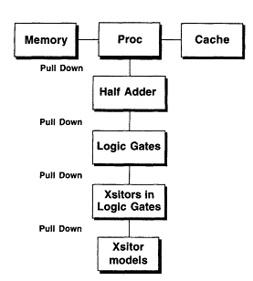
Figure 7.2 A possible hierarchical path that might be traversed during the design of a distributed processor.
An interesting point is that the digital simulations are performed in the time domain. Regeneration in digital systems is performed by a thresholding process in which, when the input voltage level passes a given value, the output shoots up to a given value, significantly above the threshold level, as fast as the circuit allows for. This technique of regeneration allows for inexpensive signal reconstruction, but is inelegant in the sense that it generates a multitude of harmonics with noise envelopes surrounding each. To simulate such a situation in the frequency domain would be, at the least, computer intensive. Further, time-domain circuit models for the nonlinear elements (generally MOSFETs) are well known and run efficiently in the time domain. An ever-growing problem in the digital simulation world, however, is the inclusion of dispersive elements, dispersively coupled lines, and other such artifacts that arise as clock rates increase. Dispersion, in general, is much easier to treat in the frequency domain than in the time domain. One could argue that it is always possible to Fourier transform frequency domain formulations but, unfortunately, the fast Fourier transform (FFT) is discrete, and windowing often precludes fidelity. Recent work on combining finite-difference time domain (FDTD) with SPICE holds promise for providing insight into simple cases of dispersive propagation, but is still too computer intensive a technique to provide a general solution to the modeling problem. The frequency-domain time-domain dichotomy is alive and well in digital modeling.
Microwave System Design
Much as in the digital world, the microwave system design process is also hierarchical, probably by example, as microwave CAD is a follow-on to digital CAD. A possible hierarchy for a microwave CAD tool may appear as that depicted in Figure 7.3. If for no other reason than its follow-on status, microwave CAD has achieved nowhere near the maturity of digital CAD. It is mature enough, however, that there do exist a number of commercial CAD tools. The popularity of some of these tools has produced a situation in that there are de facto standard microwave design procedures that are more or less followed by most of the major manufacturers of microwave systems.

Figure 7.3 Schematic depiction of a possible hierarchy for a microwave CAD system.
Typically, a microwave system will contain a microwave source, a modulation subsystem with digital control, a transmission system, at-element amplifiers, radiating/receiving antenna elements, a bank of mixers, some RF processing elements, and some analog to digital (A/D) converters leading into some digital processing electronics. A mixer subsystem may appear as the one depicted in Figure 7.4. The highest level of design is one in which the major functional design blocks are the simulation blocks. A major difference, however, between digital and analog CAD is that in analog CAD there can be no logical levels. Simulation at all levels must be carried out on waveforms. One is primarily interested in system characteristics such as frequency response and noise propagation through the system. It is the signal to noise ratio at a given frequency that determines all of the important system parameters such as dynamical range and bit error rate (false detection probability in radar) of the external digital processing circuit. At the highest level, the blocks are essentially characterized by transfer functions and noise figures, as blocks were characterized in the pre-CAD days. Indeed, if the radar were single frequency, one could easily obtain analytical results for frequency response and signal-to-noise ratio. The reason for CAD at this level, more than all else, is that systems are no longer so simple. Waveforms can be complicated as can coding and, for that matter, functionality. By having an automated system of analysis, many different schemes can be rapidly and easily analyzed.
In microwave CAD, the next level below the system (highest) level can be physical, in the sense that this next level will employ frequency-domain circuit and device models linked together by transmission lines (i.e., refer again to Figure 7.4). The circuit and device models at this level, for the most part, will exist in pull-down libraries. The libraries for the active elements more than likely will come from the foundry. Models for the passive elements likely will come from a combination of extensive fabrication and characterization as well as possibly full or nearly full wave modeling of the interconnecting, coupling, and filtering structures. It has been in this arena of passive element modeling that we have seen the most interaction between industrial designers and academic researchers. It is also in this arena that there are still
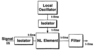
Figure 7.4 A possible realization of a microwave mixer subsystem.
extant problems with the microwave modeling process. Parasitic couplings between lines are generally small, and it is often not serious that they do not show up in the transmission line based models. This is not true when the couplings are near active elements where they can provide output to input control, system-like coupling. Yet these effects will not show up at all in the modeling process unless put in by hand by a wise design engineer who knows exactly what areas on a chip or board really need full wave modeling and which do not, and who further needs to know how to carry out the partitioning. In this sense, CAD for microwave systems is exactly that—computer aided design and nothing remotely like automated design.
An interesting point is that the microwave simulations are frequency-domain simulations. Due to propagation dispersion, one generally wants to modulate about a center carrier frequency. At a receiver, there will generally be a local oscillator that will beat down this carrier to an intermediate frequency. Power that goes into harmonics of the carrier frequency will then simply be lost in the receiver end filtering process. One, therefore, strives in a microwave system to minimize any nonlinear behaviour. In the vicinity of necessary nonlinearities, such as those inherent in mixers, liberal use of filtering techniques are employed to keep the unwanted harmonics from forming. For this reason, frequency-domain analysis, together with harmonic balance, are acceptable analysis tools. This situation is quite compatible with the transmission line models employed. Use of the frequency domain allows for inclusion of dispersion in lines, circuits, and devices. The use of the frequency domain also allows for the models to be verified. The high center frequency of microwave carriers pretty much requires the use of frequency-domain (network analyzer) based measurement techniques. Transient effects in the microwave world can only be measured in narrow bands around the center frequency and its (unwanted) harmonics. Microwave CAD is strongly grounded in the frequency domain.
Optical System Analysis
The field of optical networking is still a young field. The growth of the fiber optic network, driven by the need for a transmission medium that would fit into existing right of way, was explosive, even when compared to the ever-increasing pace of development at this point in the twentieth century. An outcropping of this pace of growth was that the point-to-point system architecture and loss budgeting techniques became pretty much frozen in from day one. A typical block diagram for an optical transmission system may appear as in Figure 7.5 and indeed loss budgeting methods are based on associating a loss factor with each of the stages and transitions appearing in this model. This is not to say that there has not been a large amount of
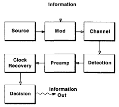
Figure 7.5 A block diagram for an archetypical optical communication system.
advanced modeling work on various components (especially lasers), nor extensive work into more advanced data communications architectures, just that the practice of link design seems to be based on some quite simple, yet formalized, design rules. (The literature indicates that in-house design programs at various optical communication groups are beginning to exist, but are not yet commercial). These rules are quite similar to those used in point-to-point RF and microwave link design (pre-CAD) and essentially track the total signal and noise power through the system (i.e., again refer to Figure 7.5). Frequency response in an optical link generally means response to the signal modulation as parameterized by the optical carrier, and also tends to be handled as the signal and noise power. The budgeting processes require loss, noise and dispersion figures for various components and channels in the system, and in this sense the design process is hierarchical, much as is the microwave design process.
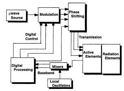
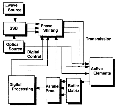
RECENT MODELING RESULTS FROM GWOL
In the present section, we discuss first some of the historical reasons for our having adopted some of the simple models we have adopted for physical devices, as well as the original ''optical communications'' model (as in Figure 7.5) that we adopted for prediction of salient system characteristics. Now, a typical phased array radar system might be represented by a block diagram such as that displayed in Figure 7.6. An optically assisted phased array radar system block diagram appears in Figure 7.7. A salient feature of that diagram is that there needs to be digital, optical and microwave modeling involved in any prediction of the operational characteristics of this microwave optical radar. As with many other groups, our first attempts to come up with accurate system modeling were aimed at simulation of as complete a subsystem as we could. To start with, rather than relying on pure computer power, we tried to use simplified models we thought could rapidly simulate large areas of our microwave optical circuits. Such a model is contained in the paper by Radisic et al. (1993). We soon found that our microwave (electrical) model was far from optimal in that it had much too much accuracy over the majority of the layout area, yet too little in certain neighborhoods (a problem that seems to be shared by many of the techniques presented by participants of this workshop). For example, the effect of parasitic coupling on passive lines is a small effect, unless one is near an active element. Various full wave as well as quasi-static methods can be used to simulate the passive lines, taking
full account of parasitics. Full wave models, however, are of no real efficacy in active regions, where the important effects are those of charge transport. To try to make a transistor model that fits into the simulation is a bit pretentious, as transistor (active device) modeling is a mature subject, and there exist excellent models for such devices, both in the time and frequency domain, which do not necessarily easily mesh with electromagnetic simulation. At some point we realized that, perhaps, the hierarchical techniques that were so ubiquitous in industrial CAD may well be the ones most applicable to our problems. We will then discuss some of our initial attempts to work with these new ideas, and then indicate some of the pitfalls we have fallen into, while emphasizing some oft he potential advantages of the approach.
Integrated optical devices, in general, consist of optical channels with electrodes running over them, to effect electrical control of optical stream. To solve exactly for the optical field exiting such a device, given the input optical field, would require a full wave electromagnetic simulation of the electrical field, which involves both the electrodes and feedlines, followed by a calculation of the time varying dielectric constant in the substrate (as caused by the electro-optic effect), and then a full wave simulation of the propagation of an optical field in a time varying dielectric medium. There arises a question of what information we really need from the model and what accuracy of prediction we can expect. In a phased array, one is interested in transforming signals back and forth from the microwave to optical domains. The efficiencies of these transformations (at a given microwave frequency) are of crucial importance. Also important are deviations from pure harmonic behavior whether they be deterministic (harmonic distortion due to nonlinear modulation transfer function) or stochastic in nature. The accuracy with which we can determine such parameters as the mask parameters, due to fabrication tolerance, or diffusion parameters, due to oven ramping or simply imprecise knowledge of the diffusion coefficient of something of finite purity into something else of finite purity, cannot ever be as good as 1 percent. For this reason, from early on we have adopted phenomenological modeling techniques. A block diagram of a phenomenological tool may have a representation such as that of the block diagram of Figure 7.8. The idea is that one uses a model that is as accurate as possible (includes as much physics as one can) but that does not rely on exact knowledge of all parameters. Instead one sets up the model with somewhat ill-determined parameters that can be calibrated on a specific fabrication line in order to specify the tool to that line. This takes out much of the uncertainty induced in the fabrication process if it is done judiciously.
Now, in integrated optical devices, unlike their microwave counterparts, one can generally ignore reflections except at discrete points (interfaces, mirrors) where the effect of reflection can generally be calculated by hand. From the fabrication models and a calibration step involving propagation constant and near field measurements, it is possible to calculate an index profile to within fabrication tolerance. One can therefore use some technique to calculate the eigenmodes in given cross sections. Further, the electrode structure is, in general, much smaller in transverse extent than the wavelength of the highest frequency component of the modulation signal. For this reason one knows that the quasi-static approximation is a good one. With these in mind, one can calculate the charge distributions cross section by cross section as well. With these approximations, it becomes possible to use coupled modes (Weierholt et al., 1987, 1988; Charczenko and Mickelson, 1989) to propagate forward the continuously varying optical mode distribution, needing only to calculate electrical/optical overlaps at each cross section in order to integrate the resulting set of first-order equations. Both simulations and experiments (Vohra et al., 1989; Charczenko et al., 1991; Januar et al., 1992; Januar and Mickelson, 1993) have shown this technique to be as accurate as any other, given the measurement uncertainties that one began with.
To illustrate the technique, we could well revisit an example that was touched on in the introduction, the example of the modeling of an integrated optical phase modulator being driven at microwave frequencies. Figure 7.9 illustrates a block diagram for a system which supplies two optical signals whose beat note is a
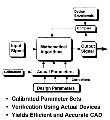
Figure 7.8 A block diagram for a phenomenological CAD tool which includes in it the possible calibration paths.
typical radar signal, a microwave carrier with phase information impressed. The system piece of interest to us here is the optical phase modulator. As was mentioned in the preceding paragraph, uncertainties in the fabrication process preclude the use of models that require sharp parameter definition. The primary processing steps necessary for fabrication of a polymeric integrated optical phase modulator are indicated in Figure 7.10. The uncertainties in this fabrication process will include polymer thickness, both due to initial spin speed as well as due to processing induced shrinkage, photolithographic errors in line definition and development, metallization thickness, and quality. All of the above are of course compounded by the amorphous nature of the polymeric material, which may cause numerous inhomogeneities. Now, the primary technique for a priori determining the behavior of the device will be an application of the coupled mode equations, which in turn requires various input data of both the electrical and optical behavior of the pieces of the device. The process is illustrated in the block diagram of Figure 7.11. The figure includes as blocks both the calibration input and the comparison with actual device blocks. The primary input block, that directly to the left of the coupled mode block, requires the input from these lower level blocks. The optical and electrical lower level blocks are schematically depicted in Figures 7.12 and 7.13. Again the calibration and comparison blocks have been included in these diagrams.
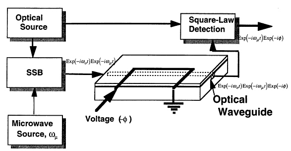
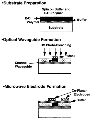
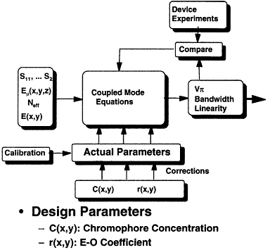
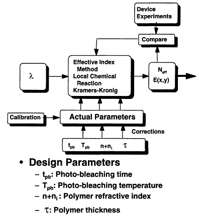
Figure 7.12 A block diagram of a lower level of the phase modulator design system of Figure 7.11, that level which is used to design the optical waveguide channels.

Figure 7.13 A block diagram of a second lower-level design subsystem of the design system of Figure 7.11, the subsystem for designing the electrode structure of the optical phase modulator.
At some point during the effort to employ integrated optics into phased array, it became clear that it was important to be able to model both the microwave and microwave optical versions of the system on roughly the same footing, for purposes of comparison. As was mentioned above, optical loss budgeting and noise propagation modeling were really taken from earlier microwave system modeling techniques. Comparing microwave Butler matrices with optical ones therefore could be performed relatively straightforwardly (Charczenko et al., 1990). It is in places where the components become dense that better modeling becomes necessary. Most joint academic-industrial efforts have concentrated on analysis of dense passive circuits where parasitics become important. Our original answer to this problem was to develop a two step approach (which we called Zoom; Radisic et al., 1993) that could replicate most of the results of full wave approaches but at a much greater computation speed. The basic idea was to first identify a parasitically coupled region, then use a static solution to find the quasi-static charge distribution that can be used to define an effective transmission line circuit that takes into account the parasitics. Integration of the first-order equations of propagation along this transmission line model could then be used to find the S-parameters that then, together with the charge distribution, can fully describe the fields throughout the substrate and surrounding space. The hope was that this technique would be sufficiently fast that it could be applied to a large area of a microwave or microwave optical circuit. A problem that arose with this idea was that the corrections on interconnect lines turned out to be rather insignificant compared to the S-parameters that would come out from a straight transmission line analysis (no added elements to represent the parasitics). This is not to say that the effects could not be dramatic. Filters can show significant frequency shifts due to parasitics as has been well illustrated by the double stub tuner (Goldfarb and Platzker, 1991). Unfortunately, filter design is a
rather mature field, one of those that would show up in the pull down menus in a VLSI system if microwave filters were a part of a VLSI system. There is not much need to simulate such things as that. Parasitic effects in the neighborhoods of active components, be they amplifiers, oscillators, mixers or what have you, could also exhibit dramatic and unpredictable effects. These are certainly worthy of simulation and study. Unfortunately, there is no easy way to take active regions of transistors into account in an electromagnetic simulation.
It was the realization that any number of commercial simulation tools could perform better active element analysis than we could practically do that really brought us to our current philosophy. It has always been clear that graphical interfaces are best purchased from a supplier. In the past, this was not so clear concerning analysis programs unless one really believed in the models included. But at this point, any number of commercial tools allow for one to define their own component models. This allows for one to develop a hierarchical modeling structure well in line with what was the original philosophy behind Zoom, and still looks quite a lot like the hierarchical techniques employed in VLSI CAD and microwave system CAD. In essence, a microwave circuit simulator (e.g., MDS, Libra, etc.) is only a tool for solving the transmission line equations that one could as well have used the first piece of Zoom (call it, for example, the circuit parameter definition part) to determine. For example, let's consider an optical link that consists of a CW laser diode, a modulator that inserts the microwave signal onto the optical carrier, a short optical propagation path, and then a receiver that consists of an optical fiber radiating into an FET that is the active element of the radiating structure, assumed to be an active antenna. The optical system block diagram of Figure 7.7 could well be applied to this system as well as a number of others. A system level model would show the blocks as the microwave source, the modulator, the link, and the active antenna. A good system level simulation package (at least two of which are commercially available) would allow one to drop to lower levels (which will presently be described) to define the system blocks, and then could perform all kinds of quite complex waveform and noise analyses quite simply. To define the blocks would require dropping first one level, to a transmission line modeling level in which the simulation, at least for the standard microwave style software, would be a frequency-domain circuit analysis. In this simulation, active components would be pulled down from standard menus, but other circuit parameters would be determined from a true physical level simulation as performed by a circuit parameter definition routine. There still is some level of art in this approach—as in areas where parasitics are important, one must still have a good idea of what areas to focus on—but at least this approach harnesses some of the power inherent in the commercial software packages. From other work presented at this workshop, the focusing problem seems to be an inherent one in modeling that cannot be attributed to hierarchical, full wave, or any other modeling technique. If there exists an inherent problem with the hierarchical scheme, it may lie in the original partitioning.
SOME CONCLUDING REMARKS
We did not want to entitle this section conclusions as this work is not concluded but only beginning. However, in addition to some differences, there are various common points that have shown up in our work and much of the other work presented at this symposium, and we deemed it appropriate to point out these commonalities (while necessarily coloring the discussion with our own bias).
A first point we would like to reiterate is that we have found that the simplest models that we have found to be reliable have been the ones that we have found to be most amenable to the phenomenological approach. For example, coupled modes together with an effective transmission line model allow one to propagate solutions forward through the system, using only the overlap of the optical and microwave fields
as a parameter in solving the first-order differential equations. Such a technique can be calibrated with physical fabrication parameter data as well as with the simplest device data of m-lines, near fields, and switching voltages. The technique that we have referred to as Zoom (which we discovered without enough study of the literature to determine its origination, but we would imagine it was with Lord Rayleigh (1945) fits well into both phenomenology and hierarchy, as it employs physical level calculations to feed a transmission line model. Models we have developed for optical injection into MESFETs have also been physical simulations to determine changes in effective circuit parameters of transistor models. We feel that it is more complex to determine the effective circuit parameters of full wave models where the circuit interpretation of the results is not so immediately clear.
The problem of choice of, as well as interfacing of, time-domain and frequency-domain tools, is a real and serious one. In the majority of the modeling work I have discussed in this talk, I have concentrated on the frequency-domain modeling we are carrying out on phased arrays. This is mainly due to the fact that we started several years ago working in the frequency domain and now that we have decided to go hierarchical, the commercial tools available are all frequency-domain tools, a characteristic of present-day microwave systems modeling. This is not to say that this is the only effort. We are also looking into digital interconnects using integrated optics. The frequency regimes of interest in the two problems are now becoming comparable, yet the tools and techniques are incompatible. This is more than a modeling problem; it is a real problem. People who model microwave systems have solutions to high-frequency propagation problems, yet work in such a different world from the digital modelers that their solutions cannot be applied to the digital world. It would be nice to see a bridge built.
A common thread in many of the works presented here has been that one must find ways to partition a large structure in order to analyze it. The point is that some regions may require totally different techniques of analysis than others. A pitfall in making the decision as to where to partition, especially strongly seen in hierarchical techniques, is that the boundary characteristics can seriously affect the system performance in a real sense, as well as the system analysis.
REFERENCES
Charczenko, W., and A.R. Mickelson, 1989, ''Symmetric and asymmetric perturbations of the index of refraction in three-waveguide optical planar couplers,''J. Opt. Soc. Am.6, 202-212.
Charczenko, W., M. Surette, P. Mathews, H. Klotz, and A.R. Mickelson, 1990, "Integrated optical butler matrices for beam forming in phased army antennas,"SPIE Proc.1217, Los Angeles.
Charczenko, W., P.S. Weitzman, H. Klotz, M. Surette, J.M. Dunn, and A.R. Mickelson, 1991, "Characterization and simulation of proton exchanged integrated optical modulators with various dielectric buffer layers,"J. Lightwave Technol.9, 92-100.
Feigenbaum, M.J., 1980, "Universal behavior in nonlinear systems,"Los Alamos Sci.1, 4-27. This paper is reprinted along with a number of other relevant papers in the collection Universality in Chaos, P. Cvitanovic (ed.), 1984, Bristol: Adam Hilger Ltd.
Goldfarb, M., and A. Platzker, 1991, "The effects of electromagnetic coupling on MMIC design,"Microwave and Millimeter Wave CAE1, 38-47.
Januar, I.P., and A.R. Mickelson, 1993, "Dual wavelength (X = 1300-1650 nm) directional coupler multiplexer/demultiplexer by the annealed proton exchange process in LiNbO3,"Opt. Lett.18, 6, 1-3.
Januar, I.P., R.J. Feuerstein, A.R. Mickelson, and J.R. Sauer, 1992, "Wavelength sensitivity in directional couplers,"J. Lightwave Technol .10, 1202-1209.
Radisic, V., D. Hjelme, A. Horrigan, Z. Popovic, and A. Mickelson, 1993, "Experimentally verifiable modeling of coplanar waveguide discontinuities,"Special Issue on Modeling and Design of Coplanar Monolithic Microwave and Millimeter-Wave Integrated Circuits, IEEE Trans. Microwave TheoryTech.41, 1524-1533.
Rayleigh, J.W.S., 1945, The Theory of Sound, New York: Dover Publications. This two-volume set is actually a reprint of an 1896 tome.
Vohra, S.T., A.R. Mickelson, and S.E. Asher, 1989, "Diffusion characteristics and waveguiding properties of proton exchanged and annealed LiNbO3 channel waveguides,"J. Appl. Phys.66, 5161-5174.
Vohra, S.T., M. Spano, M. Shlesinger, L. Pecora, and W. Ditto, 1992, Proceedings of the First Experimental Chaos Conference, River Edge, N.J.: World Scientific.
Weierholt, A.J., A.R. Mickelson, and S. Neegard, 1987, "Eigenmode analysis of parallel waveguide couplers,"IEEE J. Quantum Electron .JQE-23, 1689-1700. See also ELAB report STF44 A8611.
Weierholt, A.J., S. Neegard, and A.R. Mickelson,1988, "Eigenmode analysis of optical switches in LiNbO3: Theory and experiment,"IEEEJ. Quantum Electron.JQE-24, 2477-2490.


