


Below is the uncorrected machine-read text of this chapter, intended to provide our own search engines and external engines with highly rich, chapter-representative searchable text of each book. Because it is UNCORRECTED material, please consider the following text as a useful but insufficient proxy for the authoritative book pages.
Appendix C: High-Temperature Microwave Devices Semiconductor devices are making an ever-greater impact in system applications as they are increasingly utilized for microwave and radio frequency (RF) power generation and amplification. The history of this impact can be traced back to the early 1970s when silicon diodes were developed for microwave detection and power structures made from the III-V compound semiconductors (Ga,Al,In)-(As,P) could be fabricated resulting in material combinations in which band structures were engineered to optimize device performance. High Electron Mobility Transistors (HEMTs) and Heterojunction Bipolar Transistors (HBTs) improved on the performance of generation. The utility of the diodes extended to microwave devices. frequencies unattainable by silicon bipolar transistors that were limited by their long charging-time constants and low carrier-diffusion rates through the base layer. Silicon FETs were developed for digital applications, but their potential for microwave use was pre-empted by improvements made in gallium arsenide (GaAs) materials technology. GaAs offered high electron mobility and high saturated velocity not available with silicon and held the promise of much better microwave performance. The first GaAs devices were Gunn diodes that used the negative differential mobility available in the material. Throughout the early 1980s there was steady progress in improving the quality of GaAs wafers and devices made from them. The premier device of interest was the GaAs MESFET. Development benefited from electron beam gate writing technology established during the same time period. Gate lengths achievable for GaAs MESFETs decreased to submicron dimensions, enabling a number of high-performance applications through the millimeter-wave bands. At the same time, GaAs IMPATT diodes set records for power output. Such diodes are now combined to form units that can achieve the kilowatt level at frequencies above 30 GHz. Indeed, GaAs IMPATT diodes are a serious contender for applications now requiring vacuum tubes. In the late 1980s and early 1990s, materials technology again advanced with the widespread application of MBE and metal-organic chemical vapor deposition (MOCVD) techniques. Heterojunction 93 Concurrent with the development of improved III-V microwave devices was the development of monolithic circuit technology. For this technology, circuits necessary to tune transistors electrically and combine their power were printed directly on the same semi-insulating GaAs substrates incorporating the active devices themselves. The result was a cost and weight savings in addition to considerably enhanced functionality of the chips over discrete devices. Materials technology was again a key to the progress of the field. For integrated circuits to be cost effective, large defect-free wafers were required. These wafers were developed as the industry recognized the need for them. Development work was aided by the commercial demand for LEDs requiring GaAs substrates. In recent years, devices on indium phosphide (InP) substrates have come under development. HEMTs and HBTs on InP can have performance advantages over devices designed on GaAs substrates. This is due to the broad range of materials which can be grown hetero- epitaxially on InP. Also, compared to GaAs substrates, InP offers higher avalanche breakdown fields and higher thermal conductivity (e.g., the thermal conductivity of InP is 0.7 W/cm K; GaAs is 0.54 W/cm K). Nevertheless, microwave devices on GaAs provide the benchmarks of performance against which other materials are judged. As systems designers consider the use of solid-state microwave devices, they are confronted with the need for maintaining device temperatures low enough to ensure efficient operation and provide for reliability. In general,
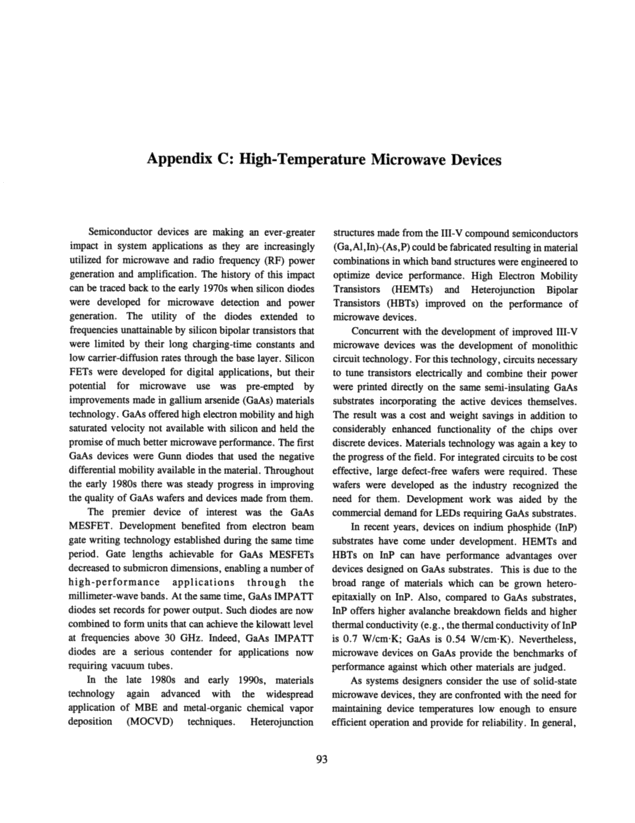
Materials for High-Temperature Semiconductor Devices operating temperatures of GaAs transistors and diodes must be held below 150-200 °C. Above these temperatures, parasitic resistance increases and saturated carrier velocities decrease, both contributing to degradations in gain performance. Furthermore, there is a significant increase in the pace of deteriorization in the contacts- and in some cases the doped layers due to elevated diffusion coefficients of particular dopants such as zinc (p-type in GaAs). Deteriorization is at least partially thermally activated, with applied voltages and currents also playing a role. The major implications of the need to limit the temperature of microwave devices are twofold: (1) power density must be limited at the active layers since much of the temperature rise is due to heat-spreading resistance (known as thermal resistance) through the substrate very near to the active regions, and (2) attention must be paid to cooling the chip mount to minimize ambient temperature rise due to the time average power dissipated. The second item has a major impact on the utility of GaAs-based devices in microwave systems. Cooling systems must be provided to remove heat from the system and maintain heat-sink temperatures at acceptably low levels. The operating temperature of the device is given by Equation (C.1) Tj = To + Rapes, (C.1) where Tj is the active-layer temperature, To is the ambient heat-sink temperature, R'h is the device thermal resistance, anal P`'js is the dissipated power. It is evident from Equation (C. 1) that higher permissible operating temperatures and lower thermal resistance will allow higher ambient temperatures in systems. This will have a favorable impact on size, weight, complexity, and cost. Furthermore, if higher operating temperatures could be utilized, circuits with higher power-dissipation densities would be allowed. For low thermal resistance, a high thermal conductivity material is required since, as noted above, most of the thermal resistance is provided very near to the active region of the device where the heat has not yet spread over a large area. lIigher permissible power dissipation Is an advantage to the system designer only if it adds functionality to the circuit (by allowing more transistors per unit area) or if it relates directly to improved power performance. This point is illustrated by expressing the dissipated power, 94 PdjS, in a transistor in terms of its gain, G. and its RF Pdis [( 1 /hD) + ( 1 /G) - 1 ] Pout , (C . 2) where PDC is the DC input power to the transistor and hD = POUL/PDC and hD is called the drain or collector efficiency depending on the transistor type. A useful parameter is the power-added efficiency (PAE) defined by PAE = (Pou' - Pj,)/PdC = hD[1 - (1/G)] . (C.3) Normalized curves of power dissipation are shown in Figure C-1 indicating sensitivity to both gain and efficiency. If a transistor with a given thermal resistance can withstand higher operating temperature but is less efficient, the ambient temperature must be reduced correspondingly and the advantage is lost. Furthermore, the prime power required by the transistor is increased, making it less suitable for use. An alternative is to reduce the output power required from the transistor. This, too, has undesirable system implications. In summary, good performance (gain, efficiency, and power output) is required from any microwave semiconductor device intended for operation at high ambient temperature. Only in rare cases will poorly performing devices be used simply to withstand high ambient temperature. The semiconducting materials discussed in this report, SiC, diamond, and III-V nitrides are candidates for use at 1 ~ _ 1.4 _ o ~cn ~1 06~l 1 1 :~0 0.2 0.2 0.3 0.4 0.5 0.6 0.7 0.8 on 1 Drain Efficiency FIGURE C-1 Contours of normalized power dissipation on the · rim. · ~ gam-ernclency plane.
Appendix C: High-Temperature Microwave Devices high temperatures according to the criteria discussed. These candidate materials can be classified as "emerging materials," as GaAs was an emerging material of the early 1970s. Thus, in assessing the potential for microwave devices constructed from SiC, diamond, and nitride materials, this appendix separates the "fundamental" properties inherent to these materials from those related to technology deficiencies that will almost certainty be overcome in the long run. This fundamental category includes such parameters as mobility, saturated velocity, dielectric constant, and avalanche breakdown electric field. Two often-cited "figures of merit" are due to Johnson (1965; JFM) and Keyes (1972; KFM). JFM accounts for the fact that in an intrinsic device (i.e., one without parasitic resistance or reactance) there is a tradeoff between the time a carrier spends gaining energy in an electric field as it drifts through a device and the response time of the device. JFM is related to electronic properties and does not account for thermal effects. JFM also does not predict the ultimate device active volume, proportional to power. A better figure of merit is KFM. Impedance considerations and the resulting increase in thermal resistance as devices are made smaller are accounted for by use of KFM. Keyes assumes that smaller devices are inherently faster in response at a fixed input impedance level. But devices cannot be made smaller without increasing the thermal resistance and thereby limiting the power output. This introduces the thermal conductivity as a factor. The breakdown field is not significant in this figure of merit since KFM addresses a thermal rather than an electronic limit. Calculated JFM and KFM for a variety of materials are shown in Chapter 3 in Table 3-1. For JFM, the high breakdown field dominates, making all of the wide bandgap materials attractive when compared to silicon, germanium, and GaAs. There appears to be no significant difference in the predicted merit among the various wide bandgap materials. The high thermal conductivities of the wide bandgap materials increase the values of KFM. Also, their lower dielectric constants reduce the capacitance per unit area thereby further increasing KFM. The figures of merit suggest that electronically limited devices such as FETs should have higher power density in the wide bandgap materials. For thermally limited devices such as bipolar transistors or IMPATTs, higher 95 power density should also be achievable in the wide bandgap devices. These predictions must be moderated by the fact that both figures of merit give a very crude picture of the situation since only the "intrinsic" device is considered. The figures of merit do not account for parasitic resistance and other detailed effects that limit gain and efficiency. The requirements of matching devices operating under bias conditions that take advantage of the material properties is also omitted from the figure-of- merit analysis. For example, is it possible to operate devices at high voltages when the necessary high impedance loads are in conflict with conjugate matching requirements for gain and efficiency? These considerations are addressed in more detail in the next section. The figures of merit just discussed are based on some of the fundamental properties of the materials. Ultimately, technology issues must be confronted. Such issues include wafer size, defect density, contact resistance, and stability of contacts at elevated temperature. Fundamental properties and technology issues are not totally unrelated, and some important factors fall between the two categories. For example, sheet resistivity and contact resistance may both be related to the alloy method and the metallurgy used to form the contacts. The choice of doping method (e.g., growth versus implantation) may relate mobility (fundamental) and doping density (technology). These relations can only be resolved in the course of time as materials, technology, and devices are developed and tested experimentally. It is difficult to make predictions of ultimate performance based on today's demonstrated technology. Instead, this appendix considers the various devices under development to highlight the relative importance to performance of physical parameters. The numbers used in the analysis are based on present-day state of the art. Since the committee is working from an incomplete knowledge of material physical parameters as a function of temperature and doping, some assumptions are made in the analysis. It is hoped that these assumptions represent the correct order of magnitude for devices that can ultimately be built from wide bandgap materials. From the analysis, it should be evident which technology elements must be given the most attention (for example, contact resistance), and this should be taken as motivation for further research and development.
Materials for High-Temperature Semiconductor Devices There are two general approaches taken to make predictions of microwave performance: detailed numerical computer models and analytic approaches. Numerical models can yield highly self-consistent results that may not represent the best global operating conditions even when optimization is attempted. The details may be inaccurate due to imperfect knowledge of the physical parameters or circuit constraints. Furthermore, such an analysis often does not clearly expose the physically important parameters. Therefore, this appendix applies the analytical approach to the most important microwave devices. BASIC DEVICE TYPES The basic microwave device types for high- temperature semiconductors are the same as those now commonly made from GaAs and silicon. Candidates are the following: (1) bipolar junction transistors (BJTs), (2) static induction transistors (SITs), (3) junction field effect transistors (JFETs), (4) metal-semiconductor field effect transistors (MESFETs), (5) heterojunction transistors (HJTs), (6) impact avalanche transit time (IMPATT) diodes. Excluded from this list are both enhancement- and depletion-mode MOSFETs (see Figure C-2), which are expected to have limited utility at microwave frequency when compared with MESFETs. Oxides tend to trap charges within them and also at the interface between the oxide and semiconductor. This condition results in the screening of the conducting channel to high-frequency excitation when the transistor is not driven into saturation as it would be in switching applications. Furthermore, MOSFETs can have poor electron surface mobility due to roughness at the oxide-semiconductor interface. If p-channel MOSFETs are used in the enhancement mode, channel access must be made by holes that have low mobility or a high parasitic resistance will result. Despite this pessimism for the potential of wide bandgap MOSFETs for microwave application, it should be noted that MOSFETs fabricated from both 6H- and 3C-SiC have shown good DC properties, even at 96 e-type conducting channel formed with positive gate bias voltage Sources ',~,`' Metal ~ ...... ~ ~ ~ . N+ well r r Gate l Metal ~, LC Oxide p-type Epi Layer _ N+ well _ p-type Substrate Region depleted of carriers for negative gate bias voltage ~ 1 \ I e-type Epi Layer \ Gate I / L ' ~ 1 N+ well ~channel N+ well High resitivity substrate FIGURE C-2 Enhancement- and depletion-mode MOSFETs. temperatures as high as 400 °C. It would be worthwhile exploring the frequency response of such devices to determine in more detail their limits of performance. Indeed, MOSFETs may have a useful role to play in low- frequency operation where the reliability at high temperatures is a primary consideration. The oxide-metal interface may be more stable with temperature than that formed between the metal and the semiconductor. Changes in that interface during long-term operation may have a less significant effect on device performance than one might encounter in a MESFET. Bipolar Junction Transistors The basic structure of the bipolar junction transistor (BIT) is shown in Figure C-3. A voltage on the base is
Appendix C: High-Temperature Microwave Devices Base Emitter L L L 1 Itl Ni Al Base Emitter ~ Base ~ I r ~n+ I |_ n+ I l d P 1 _ n+c C L~/////////////////////////~///////////////////////~ _ I' Collector FIGURE C-3 Structure of a bipolar junction transistor. SOURCE: Trew et al. (1991), ~ 1991 IEEE. used to forward-bias the base-emitter junction and charge diffuses across this junction to the reverse-biased collector-base junction. In the base, carriers are subject to bulk recombination and have a lifetime on the order of 1- 10 nanoseconds for GaAs, 3C-SiC, 6H-SiC, diamond, and GaN but not for silicon where it can be in the millisecond range due to the indirect bandgap and the low density of recombination centers. Other recombination mechanisms that depend on surface treatment are operative at the edges of the base and emitter regions, particularly at low current densities. It is expected that these effects will be related to device fabrication details and there is no proven model for them at present. The charge moving across the base of a BIT that does not recombine on its journey is accelerated across the reverse-biased collector layer delivering power to the external load. An n-p-n transistor is preferred since electron mobility, and hence diffusivity in the base, is higher than that of holes. Higher diffusivity results in higher minority carrier-density gradient in the base and therefore higher current gain. A penalty paid for this is that the extrinsic base resistance is higher in an n-p-n transistor than for a p-n-p transistor due to the lower hole mobility. There are several examples of SiC BJTs that have shown reasonable DC current versus voltage curves up to 400 °C (Palmour et al., 19931. In early work (Muench et al., 1977), n-p-n devices were fabricated from CVD layers and had DC current gain in the 4-8 range and leakage current of 10-s A/cm2 at V<e = 40 V. Although demonstrations of DC current gain is a necessary first step for a viable microwave device, the issue of frequency response is not addressed in such measurements. 97 The frequency response of a transistor is comprised of an "intrinsic" time related to the rearrangement of charge in the basic device layers and an "RC" time constant related to charging the capacitance parasitic to the transistor through parasitic resistance of the layers and contacts. Until the parasitic capacitances are fully charged, the voltages at the intrinsic device layers will not reach steady state. The intrinsic response time is characterized by the frequency at which the current gain becomes unity, fit, as I= 1/~27rf). (C.4) A second characteristic frequency is f, A the frequency at which the unilateral gain becomes unity according to Equation (C.51: U = (fmax/fl ~ (C . 5) and it can be shown that f~,a,~ is given approximately by Equation (C.6~: fn, ~ = [f~/87r(RC)] ~2 , (C.6) where R is the extrinsic base resistance and C is the parasitic base-collector capacitance. Equation (C.5) and (C.6) illustrate the importance of parasitic resistance and capacitance in determining the gain of the transistor. To reduce C, the base contacts must be small, but this, in turn, increases base contact resistance that is already high due to the low base doping required for DC current gain. The low base doping also increases the sheet resistance under the base contact and between the base contact and emitter contact. These effects severely reduce the frequency response of silicon and GaAs BJTs rendering them essentially useless above 3 GHz. Parasitic effects would have an even more detrimental effect on bipolar transistors constructed of wide bandgap semiconductors such as SiC and GaN. Bipolar transistors fabricated from diamond cannot yet be contemplated since no effective e-type dopant has been found for the material. More detailed simulations have been conducted of BJTs predicting that performance would be severely limited by ohmic contact resistance now achievable and by high base sheet resistance due to low hole concentrations
Materials for High-Temperature Semiconductor Devices necessary (Gao et al., 1994~. The base resistance would further be increased by the need to use narrow base widths (less than 500 A' to allow rapid base transit of electrons. Other simulations of SiC BJTs were conducted by Trew et. al. (1991) who showed that performance falls rapidly above 1.5 GHz (Figure Cab. Better performance is predicted from a 6H/3C-SiC HBT where a valence- band discontinuity between the two polytypes could confine holes to the base under forward bias (Gao et al., 1994~. Thus, the base carrier concentration could be increased by several orders of magnitude to up to 2 x 10~9 cm~3. In the analysis, base doping was assumed to be graded over the layer by two orders of magnitude to provide a built-in electric field and thereby speed transport of electrons across the base layer. Also assumed was a base contact resistance of 10~ Q cm2, which is a some- what optimistic value for p-type material. The results suggest that the devices at lGHz would be usable up to 450 °C (Gao et al., 19941. If base contact resistance were higher, the performance would not be acceptable. Little can be said about the potential of the other wide bandgap materials for BIT application, but the situation is likely to be similar to that of SiC. An interesting possibili- ty would be the GaAlN/GaN heteroj unction bipolar transistor, especially if constructed on a SiC substrate with high thermal conductivity. GaAlN and GaN are lattice matched over a wide aluminum concentration and the bandgap can be varied with an aluminum mole fraction between 3.5 eV and 6.5 eV. Such a heterostructure would be useful if a significant valence-band discontinuity could ~. ~ 60 a) in, ~ _ 0 ~ E ~ 50 40 ,`~ 30 ~ O O c 20 :O E a' ~ O co ~ o a _ o A Barrier height ~V4d1 Vd2 ~, . I I I ,. I I I . I . I . .1 0.5 0.7 1 2 3 5 7 10 Frequency (GHz) FIGURE C4 Simulated microwave performance of SiC BJTs. SOURCE: Trew et al. (1991), ~ 1991 IEEE. 98 be established without an excessive large conduction-band discontinuity. A discontinuity in the conduction band would lead to an energy barrier to electron injection from the emitter into the base. There would be a large collector voltage threshold voltage for turning on the transistor. Low hole mobility ~ at 50 cm2/V s) and an associated high parasitic base resistance is a potential difficulty with GaAlN/GaN heterojunction bipolar transistors. More detailed information about the properties of GaAlN/GaN combination should be obtained experimentally to asses the potential of such devices for heterojunction bipolar use. Static Induction Transistors The static induction transistor (SIT) is a three-termi- nal device that has several features making it attractive for development using wide bandgap material. The structure is shown schematically in Figure C-5. A source contact is positioned on the surface of an e-type crystal between two p-type regions. The pen junction forms a gate that, when reverse-biased, can regulate the flow of electrons from the source by raising and lowering the potential barrier seen by the carriers. This modulates the number of carriers MESFET SIT <;' S `p G Q D n GaAs~ | Sl (GaAs) l Position (channel) I ~ l u b MUG Pepsi,/ ~r ~ pS'i' _' 1 nSi . 1 _ ._ , , nSi I I D row Position (channel) Id Vd1 Vd2 Vd d' d2 vd G = Gate D = Drain S = Source FIGURE C-5 Comparison of SIT with MESFET: (a) potential gate barriers established, (b) resulting current-voltage curves for SIT, (c) generic MESFET I-V curves. SOURCE: Trew et al. (1991), 1991 IEEE.
Apper~d~c C: High-Temperature Microwave Devices collected at the drain, which is heavily doped e-type. The reverse bias established between the gate and the drain provides an electric field to accelerate the injected carri- ers. The potential barrier established by the gate and the resulting current-voltage curves are shown in Figure C-5 where they are compared with the corresponding curves for MESFETs. It is noted that the barrier height is a strong function of the applied drain voltage and that this results in a high output conductance in the I-V curves of the SIT. The current-voltage contours of an SIT resemble those obtained from a vacuum-tube triode. There is reason to believe that SITs from wide bandgap material, and particularly in SiC, can be useful for high-power application. The structure uses a vertical design in which carriers move in a direction perpen- dicularly to the crystal surface. This eliminates the requirement of submicron gate fabrication for high- frequency operation. Transit time is determined by drain- layer thickness that can be controlled and made very small during epitaxial growth. For a vertical device, there is a tradeoff between breakdown voltage and transit time. This is predicted by the JFM to be favorable for SiC compared with silicon. The devices can be operated at high drain voltages (VD = 100 V) for thick, lightly doped channels, provided that transit time through the channel does not limit frequency. In contrast to the MESFET, the current density through a SIT channel is not limited by its thickness and can be much higher when normalized to the total length of the source contact. Current density for the SIT is most properly normalized to the source contact area and described in A/cm2 rather than ma/mm. The SIT channel is depleted of carriers and has a high electric field making it more immune to space charge effects that eventually limit the current density. SITs can be fabricated on highly doped substrates. For low microwave frequencies where hybrids can be used, it is not necessary to use semi-insulating material as with the MESFET. Semi-insulating substrates would be necessary only if monolithic circuits are desired. Using conductive substrates would permit a more robust materi- als technology and allow a wider range of growth and bonding options. Frequency response could be improved since traps and defects in the substrates would be less important. The SIT is a thermally limited device. The high thermal conductivity of SiC gives it an advantage over silicon and GaAs for SITs predicted by the KFM. The 99 lower dielectric constant of SiC reduces the output capacitance per unit area of the device allowing larger devices. Also decreased is the parasitic source to gate capacitance that provides degenerative feedback and reduces gain in a manner similar to the case of bipolar transistors described earlier. The thermal and electrical advantages noted for SiC should be even more pro- nounced if diamond could be used for the SIT. The diamond application would require a suitable e-type dopant. Having considered the attractive attributes of SITs, some potential problems should be noted. The gain available is a strong function of the parasitic gate resis- tance. It is estimated that gate contact resistivity would have to be less than 1 x 1O-s Q cm2 to produce usable gain above 2 GHz. Compared to the parasitic base resistance of homojunction bipolar transistors, parasitic contact resis- tance can be reduced since base doping can be much higher. The base layer could be produced by ion implan- tation of p-type dopant. Alternatively, the p-type gate could be replaced by a Schottky contact. A problem with this approach is that sidewall metallization of the channel layer would be needed to control the potential effectively; it would be difficult to control substantial charge flow using the edge fields generated by a totally horizontal gate contact. An important issue affecting performance is the tradeoff between output-matching requirements for power and maximum available gain. This problem is an impor- tant one and is treated in more detail in the section below. Simply put, conjugate match at the output is required for maximum gain, while a different load impedance is most often required for maximum power. The output conduc- tance of a typical SiC SIT as determined from calculated current-voltage cubes is around 460 Q Em normalized to the total source length. It is predicted that SiC SITs can give up to 1.8 W/mm power density at 3 GHz at VD = 100 V. The necessary current density would then be 1.8 mA/~4m and the load impedance needed to sustain this voltage would be around 700 Q ,um. The difference in the output-matching requirements for power and gain will mean that a compromise output impedance must be found to optimize performance. It will be problematic to relinquish gain in this compromise; gain will already be at a premium for the reasons discussed above and will be further reduced from small-signal values due to nonlin- earity of the SIT and resulting gain compression. Accord
gs , 9 . Lgd Source ~I Gate I p+ i>,~,: ~///////~i1~ ~Channel, No n+ , ~! Substrate ~n - I Drain FIGURE C-6 Structure of Me Junction Field Effect Transistor (JFET). SOURCE: Clarke et al. (1993), Courtesy Westinghouse, Inc. Materials for High-Temperature Semiconductor Devices The device structure shown in Figure C-6 requires that a semi-insulating substrate be positioned below the gate to limit channel thickness. This can be a problem in wide bandgap semiconductors that do not have high resistivity substrates available. An alternative is shown in Figure C-8 where the gate is an e-type epitaxial layer placed below the channel. The channel is etched to a desired thickness and passivated with a surface oxide. This oxide must be high quality and, like the MOSFET, cannot contain traps or extraneous charge that might cause backdating effects. Furthermore, the interface between the ingly, it may turn out in practice that operating voltage of oxide and. the semiconductor must be free of scattering low-frequency SITs in wide bandgap semiconductors will sites that would reduce the mobility of carriers. be well below half the drain breakdown voltage. In contrast, the higher output impedance of FETs allow closer values of the gain and power impedance levels. Junction Field Effect Transistors In a junction field effect transistor (JFET; Figure C-6), motion of charge is controlled by a junction gate placed on the surface of the crystal in a space separating the source and drain contacts. The conducting channel is an e-type layer with doping in the 10~7 cm~3 range. Relative to the source, the drain is positively biased and the pen junction forming the gate is reverse-biased. When the gate voltage is modulated by an external signal, the thickness of the conducting channel varies, thereby controlling the current flow to the drain. Power gain is obtained. Typical current-voltage curves are shown in Figure C-7 for several temperatures. The JFET is similar to the MOSFET operating in the depletion mode. Enhancement-mode operation is not possible in the JFET since the gate would be forward biased and would draw current, increasing power dissipa tion in the gate and possibly introducing minority charge storage effects that would slow the frequency response of the transistor. An advantage of the JFET compared with the MOSFET is that surface charge at the gate junction is absent. Current moves in a channel region away from the possibility of surface scattering. A disadvantage in most semiconductors is that the low mobility of holes adds a parasitic gate resistance that can reduce gain. JFETs have ~ advantage over MESFETs in that the gate metal is farther from the active channel. At high temperature and RF power the gate metal can diffuse into the semiconduc tor and degrade the gate. JFETs could be more reliable. ~ , ~ Inverted JFETs have been fabricated (Kelner et al., 1987, 1989) from 3C-SiC on a 6H-SiC substrate. DC transconductance as high as 20 Ms/mm was obtained, but the devices could not be pinched off (the drain current was brought to zero by reverse-bias gate voltage). The transistors exhibited a high output conductance. In another experiment (Kelner et al., 1991), 6H-SiC homo-epitaxial transistors gave DC transconductance up to 17 mS/mm and could be completely pinched off with -40 V applied to the gate. DC transconductance decreased to 1.7 mS/mm at elevated temperature (400 °C) due to decreas- ing mobility of electrons in the channel. One problem with inverted JFETs in wide bandgap semiconductors is the presence of high built-in voltage (approximately equal to the bandgap). The built-in voltage partially depletes the conducting channel even with no applied gate voltage. For a given channel thickness, this lowers the maximum current available and reduces the effectiveness of short gates in pinching off the channel. Another disadvantage of the inverted structure results from the extension of the gate layer under the source and drain contacts. There is a resulting significant increase in gate capacitance, figs. This can severely reduce gain for a given transconductance, am, since fit is inversely propor- tional to figs. Metal-Semiconductor Field Effect Transistors Relatively more attention has been paid to MESFETs than any other microwave device in wide bandgap semi- conductors. Goals for MESFETs under development include producing X-band power density three times that of GaAs with power-added efficiency twice that of GaAs. DC operation of MESFETs has been demonstrated by 100
Appendix C: High-Temperature Microwave Devices 70 60 - 2 c ._ ~ 20 40 O JFET - Gate voltage = 0V T=300 K I -12V I 5 10 15 20 Drain Voltage (V) JFET 70 1 T - 473 K Gate voltage = 0V of 601 _ E ~ -1V '' ~- . ~ 1 1 -14V 1 0 5 10 15 20 a) 40 ._ 20 o 70 60 40 20 o -3v JFET T = 623 K Drain Voltage (V) Gate voltage = 0V 0 5 10 15 20 Drain Voltage (V) FIGURE C-7 Typical current-voltage curves for a JFET at various temperatures. SOURCE: Palmour (1993), Courtesy of Cree Research, Inc. many researchers over a range of temperatures up to 300 °C. Table C-1 summarizes room-temperature DC gain for various FETs of SiC. Operation of MESFETs has been simulated and samples measured for small-signal gain up to 10 GHz. Submicron gates have been used for 101 SiC. Typical measured RF results are shown in Fig- ure C-9. Measurements of power performance have been conducted by Westinghouse and Cree Research Incorpo- rated. At Westinghouse, MESFETs with frequency-of- unity maximum available gain of 5 GHz gave 2 W/mm at an operating frequency of 1 GHz. Total output power was 1 W with a drain bias voltage of 75 V. At Cree Research -5v Incorporated, 0.6 micron gate-length MESFETs of 6H-SiC had fit = 5.5 GHz and unilateral f,~,,~ = 3.8 GHz. For this device, V,~ = 45 V and Id = 126 mA; device gate width was 340 ~m. Slightly better performance was obtained from MESFETs on 4H-SiC for which An = 5.8 GHz at Vie = 20 V. One might expect that the lower operating voltage in the 4H case would result in increased fit and that this would in turn result in higher measured fma'` It was found that fit was actually reduced, however. This indicates that the improvement in fit,,,, might be attributed to the higher mobility of the 4H-polytype and the resulting lower parasitic resistance. Impact Avalanche Transit-Time Diodes GaAs IMPATT diodes have been developed in the last few years, emerging as the solid-state device giving the highest power in the microwave and millimeter-wave frequency bands (Figure C-101. The wide bandgap semiconductors have the potential to give higher power density and to operate at higher temperatures. To achieve a better view of this potential, this section first describes the general features of the IMPATT diode and its opera tion. Several material structures are possible for IMPATT diodes and are shown in Figure C-11. In its simplest form , - Ni ohmic contacts- p-type 6H-SiC substrate FIGURE! C-8 Structure of an inverted JFET in SiC. SOURCE: Palmour <1993), Courtesy Cree Research Inc.
Materials for High-Temperature Semiconductor Devices TABLE C-1 Summary of Room-Temperature DC Gain for Various Field Effect Transistors of SAC Highest Operat gm Channel Mobility ing Temperature Material Device/Mode Gate Length (I'm) (mS/mm) (cm2/V s) (°C) . . . 3C-SiC 6H-SiC 3C-SiC 6H-SiC 6H-SiC 6H-SiC 3C-SiC 6H-SiC MOSFET/ Enhancement MOSFET/ Enhancement MOSFET/ Depletion MOSFET/ Depletion MESFET MESFET JFET JFET 5 7 2.4 s 24 0.4 4 5 0.46 2.8 10 2.3 4.3 30 20 17-20 Low 46 37 21 300 560 250 650 450 750 450 450 23 23 627 SOURCE: Morkoc et al. (1994). (the single-drift diode), the structure (Masse et al., 1985) consists of a p+-n junction with an n+ contact. Under reverse DC bias, the electric field profile of Figure C-11 is established with the junction electric field sufficiently high to cause impact avalanche breakdown in the region. The electrons generated at the junction drift toward the n+ contact. If the current is limited by a high impedance bias circuit, a steady current at the breakdown voltage is maintained. If, in addition, there is an RF voltage applied, the peak voltage will generate a charge clump that moves across the e-type drift zone. The current induced in the external RF load at the fundamental frequency will be 180 degrees out of phase with the RF voltage. Thus, an effective negative resistance is established across the diode terminals at the operating frequency. In general, the drift region length scales inversely with operating frequency in order to maintain the proper current-voltage phase delay. A simplified, equivalent circuit for an IMPATT diode embedded in a microwave circuit is shown in Figure C-12. The capacitance results from the depleted drift region and the external RF circuit provides the inductance and the RF load. A parasitic series resistance is included. When the circuit is properly tuned, the reactances cancel and a self-sustaining RF current builds in the loop formed by the device and RF load. As the current grows, the diode negative conductance decreases and voltage reaches a steady state when the net resistance around the diode circuit loop is zero. This is the condition for oscillation. 102 If the load resistance is increased to a point where oscillations do not occur, the diode acts as a reflection amplifier. The parasitic series resistance depicted in Figure C-12 limits the device area and power. Compared to values in GaAs, saturation resistance, Rs, is expected to be much larger in wide bandgap materials because of generally lower mobilities and higher contact resistance. In terms of the circuit parameters defined in Figure C-12, the RF power output of the IMPATT is given by Pout = (1/21( ~ G ~ - ~ B ~ 2Rs)Vrf2, (C.7) . where I B I = 27rfeA/XD, f is the frequency of operation, e is the dielectric constant, A is the device active area, and XD is the total thickness of the depleted active layer (Adlerstein and Moore, 1981~. The voltage amplitude at the transistors terminals is Vrf. The first term in Equation (C.7) represents the power available from the intrinsic device and the second term is due to I2R losses in the parasitic series resistance. The device admittance at constant current density and susceptance are proportional to junction area while the series resistance is at best inversely proportional to area, decreasing more slowly than 1/A in most cases. Thus, as device area increases, output power passes through a maximum, eventually declining; it is important that Rs not be too large or negative resistance will not be obtained. High Rs has an
Appendix C: High-Temperature Microwave Devices increasingly damaging effect as frequency is increased. The susceptibility due to the output conductance is proportional to frequency with B = 2xfC,,, where Cd is the diode capacitance. The reduction of net negative conductance is proportional to B2 producing a strong frequency roll-off in power for an IMPATT of a given area. The problem of high Rs is compounded at the large Vrf levels required for high power or saturated oscillator operation since ~ G ~ generally decreases with increasing vrf. High parasitic resistance is a particularly troublesome, potential problem for wide bandgap semiconductors. In the past, typical specific contact resistance for SiC n+ material of l0'8 doping range is around l x l0~ Q cm2 and about 5 ~ 104 Q cm2 for p+ at the same doping. Contact resistivity on n+ material is relatively insensitive to temperature up to 400 °C, while resistivity on p+ layers decreases significantly due to increasing carrier density. Nevertheless such resistivities are two orders of magni- tude greater than for GaAs. Recently, researchers have reported contacts with an order-of-magnitude lower resistivity for both p+ and n+ contact types. Efforts should continue to further reduce the contact resistance. A more fundamental issue is the low carrier mobility of both electrons and holes in SiC. Experimental and theoretical study will be required to determine the best combination of material and contact parameters for best performance. At a given frequency, power density of an IMPATT diode is determined by its operating voltage (roughly the same as its reverse breakdown voltage corrected for space-charge effects) and the maximum temperature that can be tolerated at the junction without performance degradation or reliability problems. The maximum operating temperature usually dictates the upper bound on current in continuous-wave operation. When the diodes are operated in the pulsed mode, power density can be considerably higher since heating is truncated at the conclusion of the pulse and the IMPATT has an opportu- nity to cool between pulses. For very short pulses, a current density limit is eventually reached where space- charge effects degrade the performance. Power limitations In the pulsed mode can be overcome by using more sophisticated doping profile designs. One such design of particular importance for silicon and Gays Is double-drift Read structure (Figure C-l l). It is worthwhile to inquire if IMPATTs of wide handgap semiconductors would benefit from such designs. In a double-drift Read diode, there is a drift region for the holes as well as for the electrons. There is also a doping spike on either side of the junction that abruptly decreases the electric field in the drift region to confine the ava- aIlche zone to the region near the junction. This results in increased efficiency since a--higher fraction of the applied bias voltage is used to pull charge through the drift zones. The operating voltage of a double-drift diode 30 27 m 24 ~ 21 cry ~ 18 - c 15 c' ct car ._ - E en 12 9 6 3 o 45 40 30 - - c ._ 2C 10 _ 5 _ O _ 5 1 1111 .05 .c Bias: Vd = 45 V Id = 47.643 mA \ - Vg = -2.06 V \ 19 = -2.0238 I1A \ _ \ ~ 1 1111111 1 1 1111111 1 1 1 1~1111 .01 .1 1.0 10.0 Frequency, (GHz) I'm _ \` I'm At" I" _1 1 1111111 1 11 10 Frequency, (GHz) FIGURE C-9 Measured small-signal current and unilateral gain for SiC MESFETs. SOURCE: (a) Hobgood (1993), Courtesy Westing- house; (b) Palmour (1993), Courtesy Cree Research, Inc. 103
Materials for High-Temperature Semiconductor Devices Poor Cow - a to .1 _ .01 _ 30 20 . ~ 33 30 0 .001 · GaAs 18 O Si ~ 1.8 4 10 10 oQ j 8 1.1 1.7 10 ~ 67 02 6 o · sic o .1 ~ .05 ·IIllll I I rllllll 1 10 100 1000 Frequency, (GHz) ~ 1991 IEEE FIGURE C-10 IMPATT diode performance compared with projections for wide bandgap semiconductors. Values at points are DC-RF power conversion efficiencies. SOURCE: Trew et al. (1991), ~ 1991 IEEE. is roughly 60 percent higher than for its single-drift counterpart. Accordingly, double-drift IMPATTs have a higher power density for a given current density. Further- more, the two drift regions act as capacitors in series, resulting in a decrease in junction capacitance per unit area by nearly a factor of two. Thus, device area can be doubled with a resulting increase in power at a given power density. Given these basic elements for the operation of IMPATT diodes, and ignoring potentially high parasitic series resistance, the wide bandgap semiconductors provide interesting possibilities. SiC has potential for high power density in IMPATT operation due to the high breakdown voltages that can be achieved. Electron drift regions for SiC could be longer for a given frequency than for GaAs due to the higher saturated velocity (2 x 107 cm/s) in SiC. Of course, it would be necessary for the higher velocity to persist at elevated temperatures. There would be a decrease in the capacitance per unit area resulting from the longer drift region, and this capacitance would be further decreased by the lower dielectric constant of SiC. Larger-area diodes would be possible. Double-drift IMPATT diodes could be fabricated using SiC, but these diodes would not have equal thick- ness of electron and hole-drift regions as in GaAs since the saturated velocity of holes is quite low (0.2 x 107 cm/s in 6H-SiC and 1 x 107 cm/s In the 3C polytype; Trew et al., 1991~. Such diodes have been modeled by Trew et al. (1991), who predict the possibility of SiC IMPATTs in 104 the range of 20 to 30 GHz giving about 4 W RF power with 15-20 percent DC-to-RF conversion efficiency. According to the simulation, the efficiency of SiC devices would be poor compared to IMPATTs of GaAs above 40 GHz (Figure C-10. Low efficiency would offset the advantage of higher thermal conductivity of SiC. The low predicted efficiency for double-drift SiC IMPATTs seems to result not only from assumed high values of parasitic series resistance but also from the high DC-bias voltage needed to sustain avalanche breakdown. These voltages range from 517 V for 35-GHz diodes to 236 V at 94 GHz. Compared with this, RF voltage swings predicted in the simulations are small ~ ~ 80 V at 45 GHz). Such small terminal voltage swings are associat- ed with low efficiency that is given in the large-signal limit approximately by h = 0.72(Vrf/V~c), (C.8) where h is the DC-to-RF conversion efficiency and V~c is the operating voltage neglecting parasitic series resistance (Masse et al., 19851. From Equation (C.8) one finds h = 14 percent. In order to predict the performance of SiC IMPATT diodes more accurately, numerical simulations should be extended to larger signal. It should be determined if net negative resistance is still available given that the diode conductance magnitude varies roughly as ~G~~l/Vrf. Predictions of higher efficiency might result if higher Electric Field / Doping concentration, Ipl,lnl ~ \ . ~ Distance from junction i / \ | P n1 . _ High doping confines avalanche 1 1,, 1 P n FIGURE C-11 Material structures and electric field profiles possible for IMPACT diodes. Clockwise from upper left: single~rift flat, double-drift flat, single~rift Read, double-drift Read.
We 1DC() ~ 1 - - - IMPA11 r 1 z DIODE ~ ~ L V~ G' . I DC Circuit ~ RF Circuit Rs ' '- fir ; 1 l I L c. | ~ Diode ~ ~ RF Circuit an| FIGURE C-12 A simplified equivalent circuit for an IMPATT diode embedded In a microwave circuit. current densities were used in the simulations since resulting values of ~ G ~ would be higher. It is clear that there are some fundamental problems relating to the usefulness of SiC IMPATTs. The devices are complex, and there are many interacting factors to consider. Currently, research is being conducted on SiC IMPATTs. Performance goals at 35 GHz are 12-W continuous-wave with DC-to-RF conversion efficiency of 15 percent. As of this writing, no RF results have yet been published. Diamond is another wide bandgap semiconductor with potential utility for IMPATT diodes. Diamond has the advantage of electron and hole mobility relatively higher than that of SiC. High operating voltages would be needed at a given frequency because of the low (= 5.5) relative dielectric constant and the high values of avalanche breakdown fields. The high thermal-conductivity of diamond compared with all other wide bandgap materials allows for increased ambient temperature at a given power dissipation at the junction. It was predicted by simulation that diamond IMPATTs have superior RF output power up to 100 GHz when compared with silicon and GaAs (Trew et al., 1991~. At 100 GHz, 1.5-W power at 10 percent power-added efficiency is predicted for a double- drift diamond IMPATT. RF performance is predicted to degrade above 100 GHz due to the finite extent of the Appendix C: High-Temperature Microwave Devices avalanche region that becomes comparable to the drift- region thickness. One issue complicating the use of diamond in pulsed operation is the high activation energy of its acceptors (350 mV for boron) and possible donors. There would be a fairly strong temperature dependence of carrier concen- tration in the contact and drift regions that would vary over the length of a pulse. This effect, coupled with the relatively short thermal time constants for diamond could - result in time-varying power output. Another issue relevant to diamond is whether suitable e-type dopant can be found to construct double-drift IMPATTs. Alternative ' ly, p-type layers could be used in single-drift structures. This would not necessarily be a disadvantage for perfor mance since hole-saturated velocity is 107 cm/s, a value twice as high as for holes in GaAs. The saturation electric field for holes is around 20 kV/cm in diamond. A question that relates to all of the devices considered above is whether they offer an advantage over existing devices other than the potential operation at temperatures higher than possible with GaAs or silicon. If modest performance is acceptable at elevated temperatures and the main issue is reliability and the simplification of system heat-sinking requirements, then SiC IMPATTs could be useful. On the other hand, it would be desirable to develop the full potential of diamond IMPATT diodes since they offer performance superior to that from SiC. EXPECTATIONS FOR WIDE BANDGAP MESFETs Of all the microwave devices using wide bandgap semiconductors, MESFETs have received the most attention from researchers. MESFETs do not require a high-quality oxide for fabrication, and it is relatively simple to apply micron and submicron gates to the surface of crystals. Ideally, semi-insulating substrates are re- quired, but pen junctions can be substituted to fabricate devices for testing. Researchers have reported 6H-SiC devices with 0.6-,um gate lengths that had room-tempera- ture DC transconductance of 25 mS/mm and exhibited 14 dB small-signal gain at 1 GHz despite high parasitic source resistance (Palmour et al., 1991, 1993~. A power density of 4 W/mm and a total corresponding output power of 65 W is predicted at 10 GHz (Trew et al., |05
Materials for High-Temperature Semiconductor Devices 19911. At the present time, demonstrated performance falls far short of predictions. Predictions of performance have been based on elaborate numerical models of MESFET operation. To bring the issues into better focus, it is useful to consider the problem in simpler terms using analytical models in which parameters are normalized to materials properties (Shur, 19871. The first objective is to calculate cur- rent-voltage characteristics for MESFETs of various materials. These can then be used to estimate power and efficiency from an assumed DC load line and make comparisons. It is more difficult to calculate gain from these simple models, and for this it Is necessary to rely on more elaborate time-dependent modeling. Alternatively, gain can be estimated from equivalent circuit models that take into account parasitic resistance and reactance. Expected transistor-operating temperature rise can then be considered in conjunction with gain predictions. In addition to affecting gain, parasitic resistance can have a profound effect on the current-voltage curves, so this section first considers the intrinsic MESFET, in which behavior depends on the basic velocity versus electric field characteristics. The following analysis is concentrated on SiC as a prototype for all wide bandgap semiconductors. Later sections consider the special properties of other materials. Current-Voltage Curves Intrinsic MESFETs fall into three possible regimes, depending on whether or not velocity saturates with drain bias in the channel before p~nch-off occurs. The key parameter is a = FSL/Vpo, where Fs is the field at velocity saturation, L is the channel length, and VpO is the intrinsic pinch-off voltage given by VpO = qNDXc2/~2e), (C.9) where q is the electronic charge, ND is the channel ionized donor density, Xc is the thickness of the channel layer, and e is the material dielectric constant. The parameter a is ~ measure of the relative importance of velocity saturation and channel p~nch-off in determining the drain voltage at which the drain current saturates. Velocity versus field curves indicate that the velocity of electrons In SiC saturates at 8 x 10⁴ Vlcm, considerably higher than silicon or GaAs. From its value of a, MESFETs of each 106 material can be represented in parameter space with the axis consisting of channel doping and gate length as shown in Figure C-13. The boundary labeled a = 0.33 separates a region (to the left of the line) where current saturation with applied drain voltage results from electron- velocity saturation in the channel. Below the line labeled a = 3, current saturation results because the channel pinches off at its drain end due to voltage drop along the channel. Simple analytical models for the MESFET are available for these two cases, while the region between the boundary lines requires a more detailed treatment. Assuming 0.5-,um gates are used, Figure C-13 shows that silicon and GaAs can both be well represented by the assumption of velocity saturation. This is also the case for SiC if the channel doping is held above 3 ~ 1017 cm~3. A NO value commonly used for analysis is 2.5 x 1017 cm~3, and it would be a reasonable approximation to assume the velocity-saturation model for SiC. In contrast, GaN requires a higher electric field for electron-velocity saturation (150 kV/cm) so that shorter gates or higher channel doping is required to saturate electron velocity. In the cases of GaAs, silicon, and SiC, channel saturation can be assumed and the equations describing the current-voltage curves for the MESFET can be written in dimensionless form (Sze, 1969) with all applied voltages normalized to VpO and the drain current normal- ized to gOVpo where go = q~NDXcW/L. (C.10) 7.0 r en ~ - 0 5.0 to - ._ Q ~ 30 a) ' 2.0 1.0 t.o o.o GaN a=0.33 / / / gion for SiC gradual // ~GaAschannelapproximation . ~ 1 1 a=0.33 1 1 0.0 0.5 1.0 1.5 2.0 / siC, Region for SiC a = 0.33 /electron velocity/ / saturated in / / channel / Gate Length (microns) FIGURE C-13 'a' contours for MESPETs of silicon, GaAs, silicon carbide, and gallium nitride.
Appendix C: High-Temperature Microwave Devices 0.5 - 0.4 0.3 c ._ 0.2 0.1 o 0.35 r ~ 0.30 2 0.25 _ - ~ 0.20 _ a) <, 0.15 ·`a 0.10 fins o.oo 0.5 r ~ 0.4 _ 2 - ~_ a) ._ 0.3 0.2 O. Intrinsic channel Saturation including saturation | parasitic resistance +/ , ~ MESFET Model 0.0 1.0 2.0 3.0 4.0 5.0 6.0 7.0 8.0 Source-Drain Voltage (V) Intrinsic channel saturation I Saturation including parasitic resistance (5 ohm-mm) an/ : E ~ Silicon MESFET Model 0.00 0.40 0.80 1.20 1.60 2.00 Source-Drain Voltage (V) Intrinsic channel Saturation including saturation parasitic resistance \ (0.9 ohm-mm) ~ / n 1 at constant v9s GaAs MESFET Model 1 1 1 0.3 0.4 0.5 Source-Drain Voltage (V) FIGURE C-14 Calculated locus of dra~n-current saturation for (a) silicon carbide, (b) silicon, and (c) GaAs (win and without parasitic series resistance) In Equation (C. 10), L is the gate length (typically 0.5 ~m) md W is the gate width (typically 1 mm). The transconductance of the intrinsic MESFET is also inde- pendent of the details of the material but is normalized to go The gate bias, us, is shifted by the built-in voltage and / normalized to the pinch-off voltage: ug = (Vb; - Vg)/VpO, (C.ll) where Vbi is the built-in Schottky barrier voltage and Vg is the applied gate voltage. According to Equation (C. 11), large built-in voltages typical of wide bandgap semicon- ductors offset the effect of applied gate voltage by partially depleting the channel at zero applied-gate bias. Table C-2 summarizes the results of the model in which parameters are calculated for typical design values for three materials and a 0.5-,um gate length. Included in the lower portion of the table are assumed and calculated parasitic resistances based on an N+ contact doping density of 5 x 10~8 cm~3. Chosen dimensions for the electrode spacings are shown in the table. These dimen- sions would be typical of test devices made with standard processing technology. From the modeled values in Table C-2, the saturated drain current and associated drain voltage can be calculat- ed. Modeled saturation curves are shown for the three semiconductors in Figure C-14. For each semiconductor, two current saturation curves are shown: (1) the intrinsic saturation in the absence of parasitic resistance and (2) the extrinsic saturation using typical values of parasitic resistance. Points on these curves can be reached by varying the gate bias on the MESFET and increasing the drain bias until current saturates. A few familiar typical current-voltage curves at constant gate bias are shown for reference. A noteworthy feature of the I-V curves is that I`~s' the maximum channel current at Vg = 0, is similar for SiC and the other materials even though the saturation velocity of electrons in SiC is greater. This is so because the built- in voltage from the gate contact is higher for the large bandgap material. The precise value of this voltage depends on the Schottky metal used for the gate, but it is assumed here that the voltage is equal to about one-half the bandgap voltage in each case. In operation, higher peak currents can be obtained for all materials by driving the gate somewhat into forward bias. This is not recom- mended since doing so often has reliability implications. Another option for increasing the maximum current in SiC would be to use heavier doping levels. This would reduce breakdown voltage but would have the added beneficial effect of reducing the parasitic resistance -107
Materials for High-Temperature Semiconductor Devices TABLE C-2 Assumed and Calculated MESFET Current-Voltage Model Parameters SiC Silicon GaAs Channel doping (cm~3), NO 2.5 ~ 10~7 2.5 ~ 10~7 2.5 x 10~7 Gate width (mm), W 1 1 1 Active layer thickness (Rm), Xc 0.2 0.2 0.2 Gate length (,um), L o.5 o.5 0 5 Mobility (cm2/V s), u 250 600 4,000 Relative dielectric constant, e 10.0 11.8 12.8 Gate built-in voltage (V), Vbi 1.63 0.50 0.70 Intrinsic pinch-off voltage (V), VpO 9.0 7.9 7.1 Intrinsic transconductance (S), go 0.4 1.0 6.4 Electron saturated velocity (cm/s), VS 2.0 x 10⁷ 1.0 X 10⁷ 0.6 x 10⁷ Velocity saturation field (V/cm), Fs 8.0 x 10⁴ 1.7 x 10⁴ 0.35 ~ 104 Channel saturation parameter, cat 0.45 0.11 0.02 Metal contact resistance (Q cm2) R`o 10.0 x 10 ~1.0 x 10⁻⁶ 1.0 x 10 N+ layer sheet resistance (Q/O), Rsq 843 100 25 Transfer length (,um), LO 1.1 1.0 2.0 Net contact resistance (Q), Ro 1.3 0.13 0.11 1 Em contact length Source-gate access resistance (Q), RgS 2.5 1.0 0.16 0.5 Em gate-source spacing Gate-drain access resistance (Q), Rag 5.00 2.08 0.31 1 Em gate-drain SOURCE: Morkoc et al. (1994). between the gate to the source and drain electrodes respectively. The limits of doing this for SiC should be explored in experimental studies. A comparison of the curves in Figure C-14 shows that the saturation voltages for SiC are much higher than for GaAs or silicon and that at high currents this is dominated by the effects of parasitic resistance. Even if parasitic resistance could be reduced to zero, drain current at saturation would still be an order of magnitude greater for SiC than for GaAs. This is due to the higher electron saturation fields for SiC. When the saturation voltages are high, higher DC bias voltages must be used to obtain efficient RF amplification. Fortunately, such voltages can be achieved in wide bandgap semiconductors. For the purpose of further modeling of this effect, Figure C-14 defines saturation resistance, Rs9 as an effective lower bound for the drain voltage during high-frequency operation when the peak current Is near saturation. Because of its Importance In determining the cur- rent-voltage characteristics for the MESFET, it is worth- while to consider the origin of the parasitic resistance in 108 SiC in order to identify the technological problems to be solved. Figure C-15 shows a simple model for ohmic contact and channel resistance contributions to MESFET source resistance. The specific contact resistivity is represented by resistors in parallel while the resistance of the material underneath the contact conducts increasing current density Contact resistance Ohm-cm2 ~ .~ ~ / Sheet Resistance under contact Ohms/sq Resistance to Channel Ohm/sq FIGURE C-15 A simple model for ohmic contact and channel resis- tance contributions to MESFET source resistance.
10.0 _ ~_ E E _ o 1 _ . ct .m In a, =~ 0.1 ct a_ o Silicon Carbide _ GaAs ~ 0.0 10-4 Contact Length (cm) FIGURE C-16 Contact resistance calculated as a function of contact length for Tree materials. SOURCE: Palmour et al. (1993). toward the MESFET channel. It can be shown from this model that the contribution of the contact to the resistance in ohms is given by Ro = (Z/W) coth(L/Lt), (C. 12) where Z = (rcRsq)~'2 and L' = (rJRsq)~2' with rC being the specific contact resistivity (in units of Q cm2 while W is the contact width in centimeters) and Rsq being the sheet resistance of the contact layer in Q/square. For a contact of length L ~ > L`, further increase in L does not result in a decrease in contact resistance. In this limit, contact resistance is approximately given by Ro = Z/W. This is illustrated in Figure C-16 where contact resistance is calculated as a function of contact length for three materi- als, assuming published values of mobility (Rahman and Furukawa, 1992; Palmour et al., 1993) and e-type doping of 5 x 10~8 cm~3. In Figure C-17, contours of Z and Lit are plotted on the rc-Rs~ plane. Typical points for GaAs, silicon, and SiC are included in the figure. For particular transistors where L> > L', the product RoW can be read directly as Z in the figure. It can be seen that both GaAs and SiC benefit by making the contacts larger than 1 Em long. Note that in technology development, it is proper to concentrate efforts on both reducing contact resistivity as measured in Q cm2 as well as reducing semiconductor layer resistivity. If contacts are to survive elevated temperatures, refractory metals must be used. Contact resistivities at elevated temperatures are given for refractory metals in Appendix C: High-Temperature Microwave Devices Table C-3 (Shur et al., 19931. These values are consider- ably higher than that assumed for the 25 °C analysis. There will be a corresponding increase of the saturation voltage in the current-voltage curves. Also contributing to the saturation voltage at elevated temperatures is the fact that at doping concentrations typical of MESFET channels (2 to 5 x 10~7). mobility will decrease as temneramre Increases beyond 25 °C (Goetz et al., 1993; Shur et al., 1993~. The increase is due to increasing phonon scatter- ing. One difference between the wide bandgap semicon- ductors compared with GaAs and silicon is the larger optical phonon energy in the wide bandgap material. This difference implies a less rapid drop-off in mobility in the wide bandgap case, which might be viewed as an advan- tage. The increase in saturation voltage with increasing temperature will effect the power performance of the MESFET but, as discussed later in this section, will have a much greater effect on the gain and efficiency of the transistor. Power and Efficiency From the predicted current-voltage relationships for various materials, power performance of MESFETs can be compared. Amplifier operation is described by the switching of current from the drain supply alternately through the MESFET and the external load. The voltage at the gate supplied by the power source modulates the saturated current of the channel. In this process, the point on the current-voltage plane representing the instantaneous state at the MESFET drain moves along one of the trajectories (loadlines) shown in Figure C-18. Class A operation, for which highest Dower is obtained. is illus bated. The loadlines in the figure are appropriate to conditions of maximum RF input power level such that the gate is not driven into forward conduction or reverse breakdown at any pomt in the IlF cycle. The output power is then area-bounded by the I-V axis and the trajectory. In some computer numerical simulations, overdrive of the gate is allowed along with nonlinearities and resulting harmonics resulting in prediction of higher power densities. However, for simplicity and emphasis of the main points, this possibility is disallowed in the present analysis. A set of parameters can be defined that can be used with the current-voltage curves to model expected power and drain efficiency of the transistor from knowledge of 09
Materials for High-Temperature Semiconductor Devices the DC bias voltage and the saturation resistance, RS (Adlerstein and Zaitlin, 1991~. The model variables for power output are independent of material when they are normalized to parameters characteristic of the bias point and the current-voltage curves. External load resistance (r' = 1/g~) is normalized to Rs, drain current is normal- ized to Is = VDC/2RS, and power is normalized to PS = VDC2/~2RS). Calculated values for these parameters obtained from the power model are shown in Table C-4. MESFET size is taken to be 480 ~m, similar to that used in large numerical simulation (R.J. Trew, personal communication, 1994~. It is seen from the characteristic power Ps that some of the advantage of higher operating voltage in SiC is mitigated by the accompanying higher value of RS. Nevertheless, VDC can still be made high enough to give a power advantage to SiC. In Table C-4, an upper bound on the operating voltage is used, obtained from the breakdown electric fields for SiC, silicon, and GaAs using the equation Vb = (Em e/2qND) , (C. 13) where Em is the critical electric field at junction. For GaAs, the gate to drain breakdown, Vb, is often higher due to Gunn domain formation near the drain end of the gate. For comparison in Table C-3, however, the operat- ing voltage is (Vb-RSI~ss)/2' which is traditionally chosen to maximize the power and efficiency of MESFETs. Likewise, I6C = I~J2 was chosen to maximize the area bounded by the I-V trajectory. SiC MESFETs of two designs are listed in Table C-4. The case in the second column is taken to have channel doping of 2 ~ 10~7 as assumed for the MESFETs of the other materials. For this 480-pm-gate-width MESFET, output is around 3.9 W. ten times higher than the power available from the compara- ble GaAs MESFET in the table. To realize the high-power level predicted for this SiC design, high RF voltage amplitude is needed, and this implies that high output impedance is required. The passive microwave circuits needed to achieve these impedances could be narrow band or loss (Vandelin, 1982~. Furthermore, available substrate material may be fealty and result In a relatively high output conductance for the transistor. Output conductance Is further increased by gradual saturation of electron velocity in the chaImel. A high output conductance would imply that a low value of load resistance would be required for a conjugate ~0 match condition giving maximum gain. This is a condition in conflict with maximizing power. Making the transistor larger to reduce the power-load impedance would not diminish the ratio between the gain match and power match since both would scale with device size. Gain would already be diminished by the high parasitic source resistance in a SiC MESFET through which gate charge must be provided by the microwave exciter during the RF cycle. The discrepancy between power match at high operating voltage and gain match for SiC appears to be common to all the wide bandgap materials due to their characteristically high parasitic series resistance and high saturation voltages. Compromises must be found to optimize the load. The situation is illustrated schematically in Figure C-18. At low bias voltage, loadline "A" gives maximum gain while loadline "B" gives maximum power. At a higher bias-voltage loadline, "C" maximizes both gain and power (assuming device output conductance is not different at this bias). At the highest applied voltages, the load resistance for maximum power can become too high and there will be excessive mismatch at the output resulting in reduced gain. The discrepancy in required load impedances for power and gain could account for Me less-than-optimum results reported for power tests in discrete devices of wide baIldgap material; tuning, operating voltage, and operating current must all be compromised in the test. One way to decrease the power-load resistance at a given bias voltage is to increase ISIS and reduce the -2 - c~ E o - ,~ ~ -6 o -4 -10- 0.5 1 Ro=(ZNV)coth(ULt) z=1 0 Ohm: 0.1 Ohm-mm 0.01 Ohm-mm 1 1 1 ~1 1 1 1.5 2 2.5 3 3.5 4 Log[R sq (Ohm/square)] FIGURE C-17 Contours of constant Z plotted on rc-Rsq plane. SOURCE: Rahman and Furukawa (1992), ~ 1992 IEEE.
Appendix C: High-Temperature Microwave Devices Material Type TABLE C-3 Listing of Several Refractory Metallizations on SiC and their Contact Resistivities Contact Maximum Useful Doping Density Resistivity Temperature Metal (cm3) (Q.cm2) (oc) 3C-SiC n Ti/TiN/Pt/Au 1016 1017 1.2 x 10⁴ 650 3C-SiC n WlPtlAu 1016 1017 1.5 x 10⁴ 650 6H-SiC n TiN 1.6 ~ 10l ~4 x 10⁻² 550 6H-SiC p 3C-SiC/Al/Ti 1-3 ~ 10l ~2 x 10⁻⁵ <450 6H-SiC p Al/Ti 2 x 10¹⁹ 1.5 x 10⁻⁵ <450 SOURCE: Shur et al. (1993). operating voltage of the transistor. This will result if higher channel doping is used as shown in the first column of Table C-4 for the case where No is increased by a factor of two to 5 x 1017 cm:3. This change increases I,ISS by about a factor of two. The DC bias voltage is reduced by a factor of two as necessitated by the lower gate drain breakdown voltage at the higher doping level. The design change decreases the power load by a factor of four, bringing it into the range needed for GaAs devices of comparable size. Power density is now around 4.3 W/mm. As expected, the change in doping reduces the drain efficiency compared with the former SiC case from 46 percent to around 37 percent. This is due to the high saturation resistance of SiC despite a decrease in the channel access resistance since there is still a high knee voltage at the increased INS. The power added efficiency will decrease only slightly since the gain (taken to be 8 dB and 10 dB respectively) at full power should be higher due to the improved match achieved with the power load (Trew et al., 19911. In the detailed design of wide bandgap MESFETs, tradeoffs between the parameters j~ ~ Class A / | \ \ ~ bias i~ \ Appoint it/ ~ ~ Vd vb FIGURE C-18 Representation of current-voltage curves for a MESFET and typical loadlines for Class ~ operation. discussed above should be taken into account to optimize performance. MESFET Gain Up to this point, this appendix has considered the relationship between output power and the current-voltage characteristics of SiC MESFETs compared with silicon and GaAs. Parasitic series resistance was found to be detrimental to drain efficiency, but high power density could still be achieved given the possibility of operating at high bias voltages. To make SiC MESFETs useful, high gain in addition to high power must be achieved. Gain, defined as the ratio between RF input and RF output power, is a decreasing function of frequency. The frequency response of the basic MOSFET under small- signal conditions is represented by the equivalent circuit shown in Figure C-l9 (Englemann and Liechti, 19771. To a good approximation, at X-band and below, the input resistance, Ri, is given by Ri=Ri°+Rg+Rs, (C.14) where Ri° is the intrinsic channel resistance, Rg is the parasitic gate resistance, and Rs is the parasitic source resistance. The drain resistance, Rat, is explicitly shown to conform with the reference plane for the DC cur- rent-voltage curves. lye frequency for unity current gain, fit is given by it gm/~2xCgS) = 1/~27rtg), (C. 15)
Materials for High-Temperature Semiconductor Devices TABLE C4 Assumed and Calculated MESFET Power Model Parameters SiC SiC Silicon GaAs DC bias voltage (V), Vdc 32 75 4 8 Saturation current density (A/mm), I4SSO 0.96 0.48 0.3 0.41 (Nd = 5.0 x 101) (Nd = 2.5 x 10') Specific saturation resistance (Q mm), Rso 9 14.5 5 0.9 MESFET gate width (mm), Z o 44681 oO2430 0°.1448 o .1497 Gated saturation current (A)' Ins Saura onresis cc(Q) 30.2 04 9 Load conductance (S), g; 0.010 0.002 0.029 0.013 oa res~sta ce (it), rat 101 590 35 78 P , g' 5 0 365 0 454 0 3~3 0 477 Drain efficiency, Efd Model parameter (W), Ps 27.3 93.1 0.77 17.1 RF power delivered to load (W), Pdjs 2.7 3.9 0.1 0.4 Drain current (A), Idc 0.231 0.115 0.072 0.098 Dissipated power (W), P. 4.68 4.72 0.20 0.41 Thermal conductivity (W/cm °C), C`h 5 5 1.5 0.5 Channel temperature Rise (°C), DT 63.5 63.9 9 55.5 Power added efficiency(%),PAE 0.l3O9 0.382 o~l2ol 0.l4O9 SOURCE: Shur et al. (1993). where figs is the gate-to-source capacitance, gm is the MESFET transconductance, and tg is the transit time under the gate. Potentially, f' is higher in SiC where the saturated velocity is greater than GaAs, particularly at drain voltages just above the saturation value. At the high bias voltages required for efficient and high-power microwave operation, SiC frequency response is expected to decrease. This results since the effective gate length Gdg + ~ Lc C9S_~ vCYm(:' , ~ ~D ) < ~ Gds Cds Ym=9mei FIGURE C-l9 Small signal equivalent circuit for a MESFET. SOURCE: Englemann and Liechti (1977), ~ 1977 IEEE. ~2 should include a distance beyond the gate where the channel is depleted due to the applied drain voltage. Despite the potential of SiC, measured values of fit so far have been much lower than expected. The reason for the discrepancy is not known. It might be speculated that the presence of traps in the material, particularly between the gate and drain contacts, might significantly increase the charging time of the gate. Alternatively, the surface between the contacts may charge through high resistance and not be responsive to high-frequency voltages. Such effects would not be evident in the DC I-V curves but could be revealed by pulsed I-V measurements as they have been for GaAs MESFETs (Platzker et al., 19901. Given a value of f`, one can utilize as a gain figure of merit the unilateral gain U = (f=~/fl2. In terms of the equivalent circuit of Figure C-l9, A,, is given by f, bang = f~It2~(RiG~s) + 2 7rf~RgCdg] ill} . (C . 16) Equation (C.16) shows how parasitic series resistance reduces gain. Compared with GaAs, Gus (the output conductance) is larger in SiC where substrate leakage can be greater and the rate of velocity saturation is lower. Furthermore, the
Appendix C: High-Temperature Microwave Devices .o o.e >, c' ~ 0.6 ._ ._ LU . _ 0.4 0.2 0.0 I I 0 0.4 Thermal Resistance = 65°C-mm/W Demonstrated Performance Range r Example ~ _ - Temperature Rise = 50°C / 250°C / 300°C 0.8 1.2 1.6 2 Pout (W/mm) FIGURE C-20 Contours of constant temperature rise In He GaAs MESFET channel. SOURCE: Wemple and Huang (1982). parasitic source resistance in SiC is considerably larger than for GaAs with comparable dimensions. Thus, if SiC is to exhibit gain comparable to or higher than GaAs, fit would have to be much higher. This might imply limita- tions on the drain voltage and resulting limitations in power. The situation regarding gain is quite complicated, involving both fundamental material properties and technology issues. It is concluded that the ultimate frequency response of SiC MESFETs must be established by experiment. Thermal Properties of SiC MESFETs SiC has a thermal conductivity approximately ten times that of GaAs. This section attempts to explain, based on simple models, whether or not the higher thermal conductivity of SiC offers a performance advan- tage. The section also shows plots of the available experi- mental data relative to these predictions. To determine the performance advantage, it is noted that the temperature rise of MESFETs depends on the power dissipation and the thermal resistance of the transistor. The temperature rise in the channel can be expressed in terms of the output power, gain, and power-added efficiency according to AT = q~P~js, where P~iS is given by Equation (C.2~. Contours of constant temperature rise in the channel are plotted in Figure C-20 for GaAs and in Figure C-21 for SiC. For comparison, gain is talon to be 10 dB for which the dissipated power due to the RF input is negligible. Lee thermal resistance normalized to total gate width for GaAs MESFETs is estimated to be around 65 °C/W mm, while that for SiC is reduced in proportion to the thermal conductivity of the material and is taken to be 6.5 °C/W mm (Wemple and Huang, 19821. Consider first the GaAs contours. As power density increases, drain efficiency must increase to maintain constant operating temperature rise. The example cited in Table C-4 predicts the power point in the figure for Class A operation. The range of experimentally demonstrated results from a literature survey is seen to bracket the example in both power and efficiency (Huang, 1993~. Typical transistors show a temperature rise of 50 °C or less, indicating that GaAs MESFETs are electronically limited by available drain current and voltage rather than thermally limited. Reducing the thermal resistance of GaAs MESFETs may have a slight beneficial effect on the performance of the transistors due to higher mobility, higher electron-saturat- ed velocity, and lower leakage currents at lower tempera- tures, but it is not expected to be a major benefit. For SiC, the constant temperature rise contours are plotted in Figure C-21. Note that for a given temperature rise, higher power densities and lower drain efficiencies are allowed. Plotted on this graph are the calculated power and drain efficiencies from column 1 of Table C-3, the prediction of the model of Trew et al. (1991) for 6H-SiC, and the experimental result of Westinghouse (Clarke et al., 19931. In all cases, the temperature rise is very modest less than 80 °C. The committee's conclu- sion is that as for GaAs, the SiC MESFETs are electroni- cally limited but benefit from the higher thermal conduc- tivity of the material in that the transistors can be pushed to higher power density even with relatively low efD~cien- cy without thermal consequence. Wide Bandgap MESFETs at Elevated Temperatures Silicon Carbide Although the foregoing discussion focuses on compar- ison of GaAs MESFETs with SiC, the major conclusions would apply to a number of other wide bandgap materials, such as GaN and diamond, where low mobility and high contact resistance exist to some degree. In the analysis above, the values for these parameters were taken, optimistically, as those observed at 25 °C. As the channel temperature increases, mobility decreases. This is illus- trated in Chapter 3 in Figure 3-1 as calculated for elec I ~13
Materials for High-Temperature Semiconductor Devices Irons in undoped 6H-SiC and 3C-SiC (Shur et al., 19931. In going from 25 °C to 200 °C, the mobility of 6H-SiC decreases from 420 cm2/V s to around 120 cm2/V s. The room-temperature mobility is expected to be lower ~ ~ 250 cm2/V s) for SiC doped in the 10~7 cm~3 range where impurity scattering is Important. This is particularly true for compensated or poorly activated material. Above room temperature, phonon scattering dominates and the value of mobility at 200 °C is expected to be about 100 cm2/V s more or less, independent of doping (Goetz et al., 19931. In the foregoing MESFET analysis, the lowest reported values of contact resistance is used. At elevated temperatures, refractory metals would be required. Those demonstrated so far, which would be useful at the highest temperatures, would be expected to have resistivities well above 10-5 W cm2. Continuing efforts are required to lower the contact resistance of refractory metals. Gallium Nitride Gallium nitride is an alternative candidate for high- temperature MESFETs. GaN MESFETs have been reported in the literature with a 0.6-,um-thick channel layer (Khan et al., 1993~. Channel doping was 10~7 cm~3 and with a gate length of 4 ~m, a DC transconductance of 23 mS/mm was obtained. This material is promising because it has a higher mobility than SiC. Like GaAs, GaN has a region of negative differential mobility with quite a high peak electron velocity at 2.3 x 107 cm/s and a high saturated velocity at around 1.4 x 107 cm/s. At 200 °C, electron mobility is twice that of SiC at the same temperature (Figure 3-2 in Chapter 3~. The saturated velocity of the material is unchanged, although the peak velocity decreases steadily (Shur et al., 19931. The committee concludes that the projected gain and efficiency of GaN MESFETs will be slightly higher then their SiC counterparts at elevated temperatures once refractory metals are used. In ~ analogy with HEMT design, one option suggested for GaN is the use of alloy and heterojunction material to improve the performance of FETs at elevated temperatures. SiC can be used for substrates upon which to grow hetero-ep~tax~ally GaN or alloys containing aluminum or iridium. The thermal conductivity of SiC is about 3.8 times as large as GaN so that MESFETs made from hetero-epitaxial material could have higher power dissipation density. Another option is to fabricate "high il4 electron-mobility" transistors by creating a two- dimensional electron gas at the interface between GaN and AlGaN (Figure C-221. The doping level of the conducting channel can be reduced to a minimum. This could improve mobility in the channel, provided temperatures were not so high that phonon scattering dominated. A heterojunction PET similar in size to the MESFET described above was fabricated with a GaN channel and an AlGaN cap layer (Khan et al., 1992~. A DC transconductance of 28 mS/mm was obtained. Further experimental work would be required to assess the potential of heterojunction MESFETs in nitride systems. The usefulness of A1N in homojunction or heterojunction transistors should be determined by continuing experimentation. Diamond This section considers prospects for diamond MES- FETs. Diamond has many favorable properties. At 25 °C, electron and hole mobility, at least in undoped single crystals, are considerably higher than for the other wide bandgap materials. The material has a high breakdown electric field and a high associated avalanche breakdown voltage. Diamond has a low dielectric constant that minimizes parasitic capacitance associated with electrodes and depleted layers. It has a saturated velocity for elec- trons of around 2.7 x 107 cm/s from which potentially high values of fit should be obtained. For example, f' ~ 100 GHz should be possible with breakdown voltage of several hundred volts (Geis et al., 1987~. If MESFETs 0.5: 0.4 0) 0 3 ._ ._ UJ c c' 0.2 0.1 0.0 0 1 2 3 4 Thermal Resistance = 65°C-mrr~lW Temperature Rise = 50°C Model (Trew et al.) 10GHz6H-SiC(40V) ~/ / Example (32 V) / ~ heavy doping _ 1 00°C Westinghouse result (1 GHz, 75 V) / 300°C I 1 1 5 6 7 Pout (W/mm) FIGURE C-21 Contours of constant-temperature rise in the SiC MESFET channel. SOURCE: Wemple and Huang (1982).
Appendix C: High-Temperature Microwave Devices Gate contact metal AlGaN InGaN Undoped channel with 2D-electron gas l ~ I ~ p or i GaN FIGURE C-22 A MODFET transistor win a two~mensional electron gas at He interface between GaN and AlGaN. SOURCE: Khan et al. (1992). can be fabricated in e-type diamonds, high-frequency performance better than that predicted for SiC could be obtained. Extensive computer numerical simulation of diamond MESFETs was conducted by Trew et al. (1991~. They considered e-type transistors and found that diamond could produce a power density of 6 W/mm compared with 1 W/mm for a similar GaAs MESFET. Power-added efficiencies were comparable in the 40-50 percent range, with diamond being 10 percent more efficient than the GaAs device due primarily to a higher operating voltage. They also predicted that gain for the e-type diamond transistor would be 2 to 3 dB higher than for GaAs. This is presumably due to the lower gate-to-drain feedback capacitance resulting from the lower dielectric constant of diamond. This gain could be traded off against device size allowing for larger MESFETs constructed of diamond. Note that the option of increasing the device size signifi- cantly compared to GaAs is unique to e-type diamond since it has a much lower dielectric constant and higher carrier mobility than other wide bandgap semiconductors. It has proven difficult to dope diamond e-type. Accordingly, MESFETs fabricated to date have had p-type channels. Such devices have given relatively low transconductance of 2 ,uS/mm at room temperature, increasing to 0.67 mS/mm at 400 °C (Geis et al., 19871. There was an accompanying increase in maximum channel current at the elevated temperatures that is attributed to increasing activation of acceptors (boron) that have activation energy of around 350 med. In determining material conductivity as a function of temperature, the increased number of holes overcomes the decrease in mobility, which is a strongly decreasing ~5 function of temperature. Shin et al. (1993) have estab- lished a model using a harmonic balance technique and a numerical simulator to compare the expected performance of p-type diamond MESFETs with that of e-type (nitro- gen-doped) SiC at elevated temperatures. They assumed a mobility dependence on temperature of T-g where g = 1.3 for 6H-SiC and g = 2.8 for boron-doped diamond. In both cases, contact resistivities were assumed to be 1 x 10⁻⁵ Q cm2. For the SiC MESFET, RF perfor- mance was found to be near optimum at 25 °C with 3.5 W/mm. Performance degraded with increasing tempera- ture. Gain at 8 GHz was predicted to be 16.5 dB and power-added efficiency was 44 percent for a device with 1-mm total gate length. In contrast, increasing the temper- ature of the diamond MESFET resulted in improved performance up to 680 °C. Maximum channel currents were considerably lower in diamond. At 500 °C, the p-type diamond MESFET was predicted to give power density of 0.75 W/mn' at 5 GHz with 33 percent power- added efficiency and around 8-dB gain. It was concluded that SiC MESFETs were preferred over p-type diamond MESFETs at elevated temperature. One method that has been suggested for increasing the channel current of p-type diamond MESFETs is to increase the doping density. This can be done near room temperature, however, only with sacrifice of mobility due to severe impurity scattering of holes. For example, at 25 °C, an atomic boron concentration of 10~9 cm~3 is required to obtain an activated carrier concentration of 10~5 cm~3. The resulting mobility at this concentration is reduced by a factor of eight from that obtained for undoped material. Despite the difficulties described above in using diamonds for MESFETs, the material still has consider- able promise. Future work should be aimed at finding alternative doping methods, particularly for e-type material, and developing contacts that withstand high temperatures and have low resistivities. REFERENCES Adlerstein, M.G., and E. Moore. 1981. Microwave properties of GaAs IMPATT diodes at 33 GHz. Pp. 375-384 in Proceedings of the 8th Biennial Confer
Materials for High-Temperature Semiconductor Devices ence on Active Microwave Semiconductors and Circuits. Ithaca, New York: Cornell University Press. Adlerstein, M.G., and M. Zaitlin. 1991. Cut-off opera- tion of heterojunction bipolar transistors. Microwave Journal 34~91: 114-125. Clarke, R.C., R.H. Hopkins, C.D. Brandt, M.C. Driver, D.L. Barrett, A.A. Burk, G.W. Eldridge, H.M. Hobgood, J.P. McHugh, P.G. McMullin, R.R. Siergiej, and S. Sriram. 1993. Paper presented at the 1993 IEEE/Cornell Conference on Advanced Con- cepts in High Speed Semiconductor Devices and Circuits, Ithaca, New York. Englemann, R., and C. Liechti. 1977. Bias dependence of GaAs and InP MESFET parameters. IEEE Transac- tions on Electron Devices ED-24~11~: 1288-1296. Gao, G.B., J. Sterner, and H. Morkoc. 1994. High- frequency performance of SiC heterojunction bipolar transistors. IEEE Transactions on Electron Devices 41(7): 1092. Gels, M.W., D.D. Rathman, D.J. Ehrlich, R.A. Murphy, and W.T. Lindley. 1987. High-temperature point- contact transistors and Schottky diodes formed on synthetic boron-doped diamond. IEEE Electronic Devices Letters 8~81: 341-343. Goetz, W., A. Schoner, G. Pensl, W. Suttrop, W.J. Choyke, R. Stein, and S. Leibenzeder. 1993. Nitro- gen donors in 4H-silicon carbide. Journal of Applied Physics 73~71:3332-3338. Hobgood, H.M. 1993. Growth of Large Diameter SiC Crystals. Presentation to the Committee for High- Temperature Semiconductor Devices, Washington, D.C., September 29-30. Huang, J. 1993. Proceedings of the MTT-S Microwave HBT and HEMT Workshop, Atlanta, Georgia. Johnson, A. 1965. Physical limitations on frequency and power parameters of transistors. RCA Review 26: 163-177. Kelner, G., S. Binari, K. Sleger, and H. Kong. 1987. Beta-SiC MESFETs and buried-gate JFETs. IEEE Electron Devices Letters 8~9~:428-430. Kelner, G., M. Shur, S. Binari, K. Sleger, and H.S. Kong. 1989. High transconductance SiC buried-gate JFETs. IEEE Transactions on Electron Devices 36: 1045-1049. Kelner, G., S. Binari, M. Shur, and J. Palmour. 1991. High temperature operation of alpha-silicon carbide ~6 buried-gate junction field-effect transistors. Electron- ics Letters 27: 1038-1040. Keyes, R.W. 1972. Figure of merit for semiconductors for high speed switches. Proceedings of the IEEE 60:225. Khan, M.A., R.A. Skogman, J.M. Van Hove, D.T. Olson, and J.N. Kuznia. 1992. Atomic layer epitaxy of GaN over sapphire using switched metalorganic chemical vapor deposition. Applied Physics Letters. 60:3027. Khan, M.A., J.N. Kuznia, A.R. Bhattarai, and D.T. Olson.1993. Metal semiconductor field effect transis- tor based on single crystal GaN. Applied Physics Letters 62:1786-1787. Masse, D., M.G. Adlerstein, and L.H. Holway. 1985. Millimeter-wave GaAs IMPATT diodes. Pp. 291-370 in Infrared and Millimeter Waves, Vol. 14 K.J. Button, ed. New York: Academic Press. Morkoc, H., S. Strite, G.B. Gao, M.E. Lin, B. Sverdlov, and M. Burns. 1994. A review of the large bandgap SiC, III-V nitride, and ZnSe based II-VI semiconductor device technologies. Journal of Applied Physics Review 76~3~:1363-1398. Muench, W., P. Hoeck, and E. Pettenpaul. 1977. Silcon carbide field effect and bipolar transistors. Pp. 337-339 in IEEE Digest, International Electron Device Meeting. Palmour, J.W. 1993. Design and Fabrication of SiC Devices. Presentation to the Committee on Materials for High Temperature Semiconductor Devices, Washington, D.C., September 30. Palmour, J.W., S. Kong, D.G. Waltz, J.A. Edmond, and C.H. Carter. 1991. 6H-SiC transistors for high temperature operation. Transactions of the First International High Temperature Electronics Confer- ence. pp. 511-518. Palmour, J.W., J.A. Edmond, H.S. Kong, and C.H. Carter, Jr. 1993. 6H-silicon carbide devices and applications. Physica B 185:461-465. Platzker, A., A. Palevsky, S. Nash, W. Struble and Y. Tajima. 1990. Characterization of GaAs devices by a versatile pulsed I-V measurement system. Pp. 1137-1142 in IEEE MTT-S International Microwave Symposium Digest, Vol. 3. Rahman, M.M., and S. Furukawa. 1992. Silicon carbide turns on its power. IEEE Circuits and Devices 22-26.
Apper~c C: High-Temperature Microwave Devices Shin, M.W., G.L. Bilbro, and R.J. Trew. 1993. High temperature operation of N-type 6H-SiC and P-type diamond MESFETs. Pp. 421-430 in Proceedings of the IEEE/Cornell Conference on Advanced Concepts in High Speed Semiconductor Devices and Circuits. Shur, M. 1987. GaAs Devices and Circuits. New York: Plenum Press. Shur, M., B. Gelment, C. Saavedra-Munoz, and G. Kelner. 1993. Potential of wide bandgap devices for high-temperature applications. Pp. 465-470 in Pro- ceedings of the 5th International Conference on Silicon-Carbide and Related Materials, Washington, D.C., November 1-3. Philadelphia: Institute of Physics Publishing. Sze, M. 1969. Physics of Semiconductor Devices. New York: John Wiley & Sons. ~7 Trew, R.J. 1994. Personal communication to W.J. Choyke. Trew, R.J., J. Yan, and P.M. Mock. 1991. The potential of diamond and SiC electronic devices for microwave and millimeter-wave power applications. Proceedings of the IEEE 79~51:598-620. Vandelin, G.D. 1982. Small-signal and nonlinear applica- tions for GaAs FETs. Pp. 407 in GaAs FET Princi- ples and Technology. J.V. DiLorenzo, ed. Dedham, Massachusetts: Artech House, Inc. Wemple, S.H., and H. Huang. 1982. Thermal design of power GaAs FETs. Pp. 313 in GaAs FET Principles and Technology. J.V. DiLorenzo, ed. Dedham, Massachusetts: Artech House, Inc. \