
4
Engines of Progress: Semiconductor Technology Trends and Issues
William J. Spencer
Charles L. Seitz
William J. Spencer
Everyone knows the adage (variously attributed to baseball managers and ancient Chinese philosophers): ''It is difficult to predict, especially the future.'' With that in mind, this paper focuses on how productive the semiconductor industry has been over the past 50 years, its status in 1995, the road map for the industry for the next 15 years, some of the challenges that the industry faces, a few predictions, and a final caveat.
The productivity of silicon technology is usually measured in the cost reduction of memory or the increase in processing power. The cost of memory will have fallen by roughly five orders of magnitude from 1972, when the first 1,000-bit static random access memory chip (SRAM) was available, to the year 2010, when the 64-gigabit dynamic random access memory chip (DRAM) will be available. The cost of computing has also decreased dramatically during this time frame. Fortune, the impeccable source of reliable information, recently showed that the cost of MIPS has declined by a factor of 200,000 over 30 years. This dramatic reduction in cost or increase in computing power over a period of several decades is unparalleled in any other industry. It is this continual improvement in productivity in silicon integrated circuits, and the related lower cost of memory, computing power, and communications bandwidth, that is leading the world into the Information Age.
The productivity gains are made possible by continued technology improvements in the manufacture of silicon integrated circuits. The silicon transistor has been the principal element in this technology since 1957. The types of transistors have changed from grown junction to planar, from bipolar to metal oxide semiconductor (MOS), but the transistor effect has been the principal element in all silicon integrated circuits for the past 40 years and probably will continue to be for at least another quarter of a century.
The technology changes that have occurred are listed in Table 4.1. These begin with the invention of the transistor at Bell Labs-Western Electric in 1947 and continue through the introduction of ion implantation, reactive ion etching, optical steppers for lithography, e-beam mask making, and a variety of other technologies. Except for some of the design and simulation packages, these technology innovations have all come from industrial labs. Some of these laboratories do not exist today; others have been downsized and redirected. This represents a major challenge for our industry that I want to come back to later in this presentation.
In 1995, most leading-edge semiconductor manufacturers were using a 0.35-micron technology for manufacturing MOS devices in microprocessors, memory, and logic. A cross-section of a CMOS transistor pair in this technology is shown in Figure 4.1. Silicon chips today contain as many as 20 million of these transistors. This
TABLE 4.1
Major Semiconductor Innovations
|
Innovation |
Laboratory |
Year |
|
Point contact transistor |
Bell Labs-Western Electric |
1947 |
|
Single-crystal growing |
Western Electric |
1950 |
|
Zone refining |
Western Electric |
1950 |
|
Grown junction transistor |
Western Electric |
1951 |
|
Silicon junction transistor |
Texas Instruments |
1954 |
|
Oxide masking and diffusion |
Western Electric |
1955 |
|
Planar transistor and process |
Fairchild |
1960 |
|
Integrated circuit |
Texas Instruments, Fairchild |
1961 |
|
Gunn diode |
IBM |
1963 |
|
Ion implantation |
|
|
|
Plasma processing |
|
|
|
E-beam technology |
|
|
|
SOURCE: John Tilton, Brookings Institution, Washington, D.C. |
||
technology has several interesting characteristics. The interconnect is still principally aluminum, although it is now alloyed with copper and titanium. The interlayer dielectric is still silicon dioxide. You will note that this plasma-enhanced chemical vapor deposition of silicon dioxide leaves very uneven layers. There is a complex metallurgy in the vias that consists of titanium and titanium nitride with tungsten as the principal conductor.
Today, the semiconductor industry is roughly a $200 billion-per-year industry; $150 billion of this is in the sale of semiconductor devices, roughly $30 billion in the sale of processing equipment, and approximately $20 billion in the sale of manufacturing materials, including silicon, mask blanks, photoresists, and production gases and liquids (Table 4.2). In the 1990s, the industry has grown at an extremely rapid rate, averaging more than 30 percent per year over the past three years. The industry is projected to grow at an average rate of about 20 percent per year for the next 15 years.
If we compare the growth rate of the semiconductor industry (about 20 percent per year) with the gross domestic product (about 2 percent per year), by the year 2019 semiconductor sales will be equal to the U.S. gross domestic product of $11 trillion. This leads me to prediction 1: The increase in semiconductor sales will flatten before the year 2019.
The U.S. semiconductor industry has developed a road-mapping process that looks at technology needs for the industry 15 years into the future if costs are to continue to decline. An example of the content of this road map is shown in Table 4.3. The road map considers memory, high-volume logic, and low-volume logic. The year represents the first shipment of a product with the given technology. A major consideration of the road map is cost. The cost per transistor for each of these products is predicted to decline with each generation of technology. This leads to prediction 2: There is no physical barrier to the transistor effect in silicon being the principal element in the semiconductor industry to the year 2010.
Although the road map projects technology generations for 15 years in the future and the technology required for that projection, it does not define solutions for all of the technology requirements. Let us look at some of the challenges that must be addressed to meet the road map projections to the year 2010.
Will it be possible to design 100 million transistor logic circuits and 70 to 75 billion transistors on memory chips? Figure 4.2 describes what the semiconductor community has called the design productivity crisis. The upper curve shows the compound complexity growth rate in silicon integrated circuits at roughly 60 percent per year. The lower curve shows the compound design productivity growth at about 20 percent per year. This leaves a considerable gap in 1995 and a growing gap into the twenty-first century, which is the consensus of a group of design experts in industry, government, and universities. There is no complete solution to this design dilemma. There is cooperative work on building an open infrastructure that will allow interoperability of commercially available design tools and of those tools that are developed as competitive capabilities in integrated circuit
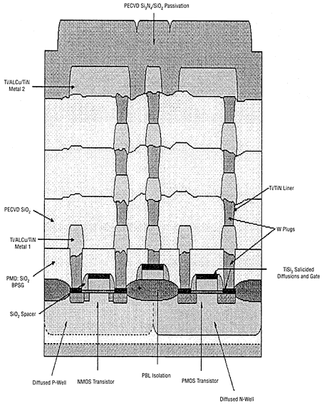
Figure 4.1
Device cross section, SEMATECH's 0.35-µm CMOS process. Source: SEMATECH.
manufacturers. The design costs, the size of design teams, and the time required to design products at the end of this century will be major barriers to continued growth of the integrated circuit industry. This uncertainty in design costs and investment to manufacture new integrated circuits has led to numerous joint ventures focused on new products.
Supposing we are able to design integrated circuits in the twenty-first century, will we be able to manufacture them? Here, I would like to focus on just one processing step, lithography. Lithography and interconnect represent the two major costs in the manufacture of integrated circuits. Figure 4.3 shows the road map for lithography and some potential solutions for lithographic requirements. At 0.35 micron and 0.25 micron, the technology choice has been made. Deep ultraviolet (DUV) exposure tools, operating at 248-nm wavelength, will
TABLE 4.2
Semiconductor Industry—1995
|
Sales |
Billion Dollars |
|
Semiconductors |
˜ 150 |
|
Equipment |
˜ 30 |
|
Materials |
˜ 20 |
|
Total |
˜ 200 |
TABLE 4.3
Overall Roadmap Technology Characteristics—Major Markets
|
Year of First DRAM Shipment |
1995 |
1998 |
2001 |
2004 |
2007 |
2010 |
|
|
Minimum Feature Size (µm) |
0.35 |
0.25 |
0.18 |
0.13 |
0.10 |
0.07 |
Driver |
|
Memory |
|
|
|
|
|
|
D |
|
Bits per chip (DRAM/flash) |
64 million |
256 million |
1 billion |
4 billion |
16 billion |
64 billion |
|
|
Cost per bit @ volume (millicents) |
0.017 |
0.007 |
0.003 |
0.001 |
0.0005 |
0.0002 |
|
|
Logic (high-volume: microprocessor) |
|
|
|
|
|
|
L (µP) |
|
Logic transistors per cm2 (packed) |
4 million |
7 million |
13 million |
25 million |
50 million |
90 million |
|
|
Bits per cm2 (cache SRAM) |
2 million |
6 million |
20 million |
50 million |
100 million |
300 million |
|
|
Cost per transistor @ volume (millicents) |
1 |
0.5 |
0.2 |
0.1 |
0.05 |
0.02 |
|
|
Logic (low volume: ASIC) |
|
|
|
|
|
|
L (A) |
|
Transistors per cm2 (auto layout) |
2 million |
4 million |
7 million |
12 million |
25 million |
40 million |
|
|
Nonrecurring engineering cost per transistor (millicents) |
0.3 |
0.1 |
0.05 |
0.03 |
0.02 |
0.01 |
|
be required for these two generations of integrated circuits. At 0.25 micron, there is a possibility of additional optical enhancement (OE) through off-axis illumination, phase shift masks, and other optical tricks. At 0.18-micron technology, the solutions are less clear, and for technologies of 0.13 micron or less, it is even less clear which technology will be suitable for production of these devices.
The development of this technology does not come for free. Projected development costs for lithographic systems (including exposure tools, resists, metrology, and masks) at 193-nm exposure wavelengths total nearly $350 million for the 1995-2001 period (costs are highest in the first four years and peak in 1996-1997). This cost is beyond the capability of any single company. This has been an area in which the U.S. semiconductor industry and the supplier industry have worked cooperatively to develop 193-nm lithography and possible optical extensions down to 13 nm. Multicompany consortia have focused successfully on technology development, whereas it is principally bilateral joint ventures that focus on new products.
Now, if we can design (still uncertain) and fabricate (possible) integrated circuits with 100 million transistors, will it be possible to package them? In 1995, 10 million transistors were being built on a single chip with a cost per transistor of about 10 microcents for a total chip cost of roughly $10. The packaging costs in 1995 represent somewhere between $5 and $35 for packages with up to 500 pins. This supports personal computers that cost in the range of $2,000 and provide moderate data capability, no voice, and very slow video. Six years from now, there will be nearly 50 million transistors on a single chip at a cost roughly five times less, with a chip cost that is still about $10. The packaging costs will rise to nearly $50 for packages with up to 1,000 pins. The question is whether this technology will provide components at a cost low enough to keep personal computer prices at roughly $2,000 with better data capability, limited voice, and faster video. The challenge of programs in the government and at SEMATECH is to bring packaging costs down so that they remain on the same level as chip costs. This will require a reduction of roughly two times the package cost.
We have looked at the challenges in design, processing, and packaging of integrated circuits during the first decade of the twenty-first century. What will the cross section of one of these integrated circuits look like? The cross section shown in Figure 4.4 is of a 0.10-micron CMOS process for high-performance logic. There are several major differences between this and the 0.35-micron schematic shown earlier. Notice that the interlayer dielectrics are all flat. This means that the dielectric material has been planarized after it has been deposited. The material has changed from silicon dioxide to a low dielectric constant polyimide. Metallization has gone to copper, with copper plugs in the vias and copper in the liners. All of these new technologies will require extensive design and testing to ensure continued reliability and cost reduction.
Typically, the interdielectric layers are on the order of 1 micron in thickness, while the gate lengths are a tenth
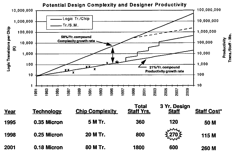
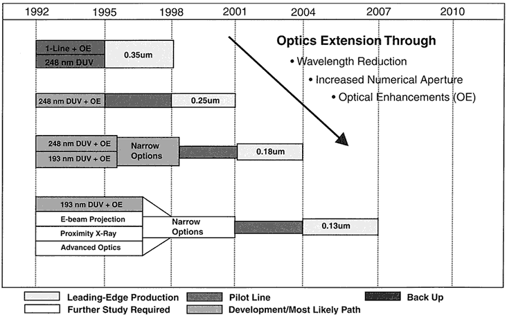
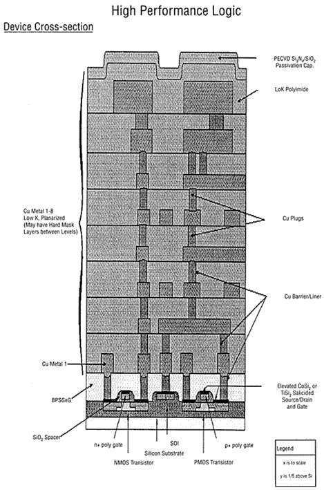
Figure 4.4
Device cross section, 0.1-µm CMOS process schematic. Source: SEMATECH.
of a micron. Thus, the schematic in this figure is compressed in the vertical direction and highly expanded in the horizontal direction. If we look at the actual cross section of this 0.10-micron CMOS process it looks more like a skyscraper. This shows why the major complexity in future integrated circuits will be focused on interconnects and the lithography to produce these interconnects. The basic transistor structure, while becoming more difficult to manufacture, will be a much smaller part of the total processing costs compared with the interconnect.
Finally, let us look at the total cost of building a manufacturing facility for future integrated circuits. The costs in 2000 are expected to be about $2 billion for each new fab. In 1970, Intel built its first fab for less than $5 million. The cost of fabrication facilities is growing faster than the growth of semiconductor revenue. This leads to my third prediction: The entire world's requirements for silicon integrated circuits will be built in a single fabrication facility, (probably Korean) by the year 2050.
Let me go back to a point made earlier in looking at technology changes that have led to the continued productivity growth of integrated circuits and where those technology changes originated. Most of the technology used in the manufacture of modem semiconductors came from industrial laboratories such as Bell Labs, IBM, Texas Instruments, Fairchild, and Phillips. Today, these laboratories either no longer exist or have been significantly downsized, particularly in physical science research. The remaining research is focused on corporate needs,
not industry needs, leaving a major technology gap. Without these engines of innovation, the entire semiconductor industry will stall in the first decade of the twenty-first century, and this stalling will slow the growth of computers and telecommunications. There is certainly enough technology to keep the industry going over the next 5 and perhaps 10 years. Beyond this time, there will be serious shortages in design, process, packaging, and other technologies that support the semiconductor industry. This is an issue that must be addressed by the industry, the government, and the universities. There is no simple solution. The semiconductor industry is looking at tripling its investment in university research. Even with this investment, there must be changes in commercialization, culture, management, and education to provide the future source of innovation for the semiconductor industry. This leads to my final prediction: All of the earlier predictions are wrong!
As soon as a road map is written down, it becomes outdated. This industry moves so rapidly that it is impossible in any document, talk, or paper to predict where it is going. Usually, the industry has moved more quickly than predictions. Engineers and scientists have typically found ways to overcome technology barriers, the industry has continued to grow at an amazing rate, and productivity continues to increase at 25 to 30 percent per year in silicon technology. This has led to the semiconductor industry as the economic driving force for the Information Age. If it stalls, the applications that are dependent on silicon technology will stall as well. This touches every aspect of our lives, from education to work to leisure. Silicon technology is pervasive in all our lives. You probably have a half dozen or more integrated circuits on your person today—in your watch, beeper, cell phone, and electronic notebook—and if you carry a laptop, of course the number goes up dramatically. There are answers to most of the manufacturing productivity issues for semiconductor technology; the major question will be where our future innovations originate.
Charles Seitz
A remarkable thought—continued progress through at least 2010. The progress described by William Spencer reminds me of neighbors who ask, "Should I buy the new model XYZ computer that just came out, or should I wait another year because they keep getting better and better?" The only answer I have for that question is, "It depends on whether you want a computer to use over the next year."
It has become part of everyone's expectations that computing devices will keep getting better and better. Bill and I are struck by the extent to which the real engine of progress is found in some of the lower levels of computing technology, even though the effect of these steady improvements is to be able to support larger and larger software packages that do more and more.
I am going to take you straight to a designer's eye view of a chip. If you were to walk around the design laboratories at places like Intel and Motorola, or at any of thousands of small companies, you would see people sitting in front of computer screens in cubicles, much like the Dilbert cartoons, with pictures or portions of a chips layout in front of them.
These pictures, like most arcane art, may be a little difficult to interpret. What the designer is looking at is a number of different layers, each in a different color, as if from a skyscraper looking down at a city. Differently colored layers represent layers of metal on a chip. These metal layers are entirely for interconnection. Special symbols, such as boxes with stipple or cross patterns, are used to indicate the connection from one of the metal layers down to another or from the metal layers down to the deeper layers. It would not surprise you, perhaps, that the wider metal layers carry power to the inner circuits of the chip. "Where are the transistors?" you ask. Well, they are in the smallest features hidden way down at the lowest levels of the chip.
To the designer, the transistor is formed where one of the wires—called poly because they were once polycrystalline silicon, although they are now typically composed of tungsten silicide—crosses another wire, the diffused area, down in the very, very tiny and deepest parts of the chip.
The layout of all of these geometrical shapes creates a data file from which optical masks (or reticles) are made, from which chips are made in turn. In this sense, all of the wonderful work that is done in semiconductor manufacturing can be thought of as similar to what the photography industry does. Designers can produce any pattern they want and turn it over to a fabrication facility that can make chips with the same pattern. Although
processes for certain types of chips are somewhat specialized, for the most part the fabricator does not use a different process for one kind of chip or another, any more than a printer might use a different kind of paper for a photograph of your daughter or your boat.
"In actual fact," as they say in England, this picture [displayed at the symposium] is not an entire chip. The plot is of an area about a quarter of a millimeter on a side. One of the aspects of chip design that I want to emphasize is complexity, and I will use every opportunity to do so. Remember, Cato the Elder kept repeating to the Roman Senate that Carthage must be destroyed. If you keep repeating something, it oftentimes happens.
So, please excuse the repetition, but these chips are awesomely complex. A state-of-the-art chip today is about 2 cm on a side. Thus, at the scale of this plot, it would take 6,400 of these pages to display the geometry of the entire chip. It is difficult for the designers even to find their way around such chips, let alone to design them.
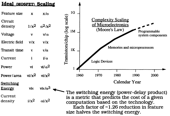
One of the beautiful things about semiconductors is that they are just physics at the lowest level. You might say, "Why do Bill Spencer and SEMATECH go to such great effort and expense to figure out how to reduce the feature size a little bit more?" Let me try to explain, based on the tabulation along the left side of Figure 4.5.
Starting in the early 1970s, device physicists recognized an ideal form of scaling of the so-called MOSFET (metal oxide semiconductor, field-effect transistor) technologies, in which transistors are formed longitudinally along the surface of the chip. Here is the basic story.
For a scaling factor a, reduce the feature size x to some value x/a . If you do this, you should also reduce the voltages in order to keep the electric fields from increasing; otherwise, you are asking someone to invent new materials that could withstand higher electric fields. (Although chips operate from relatively low voltages, the dimensions are also very small, resulting in electric fields that approach the limits of the dielectric strength of the glass (silicon dioxide) insulator under the MOSFET transistor gate.)
With electric fields being constant in this scaling, and with the mobility of silicon being constant, the velocity of mobile carriers—electrons or holes—is more or less constant. However, the carders can traverse the smaller transistor in less time, making the smaller transistors (and circuits, if you go through the entire analysis) faster. Every child knows that smaller things are faster.
The reduction in feature size increases the circuit density quadratically with the scaling factor, but if the current is also reduced in proportion, the power per device is reduced quadratically with the scaling factor. It is fortunate that these effects balance, so that the power per unit area remains constant in scaling.
The switching energy, also known as the power-delay product, is a technology metric that closely predicts the cost of a computation implemented in a given technology. The bottom line is that the switching energy, the product of the power per device and the transit time, scales as the third power of the scaling factor. Thus, for example, all of the effort of reducing the feature size by a small factor such as 1.26 pays off by reducing the switching energy by a factor of 2, and this factor of 2 can be applied across the board in all kinds of computing and communications devices. It allows chip and computer designers to offer about twice as much computing at the same cost, or the same amount of computing at half the cost.
Higher circuit density together with larger chips has led to the remarkable complexity scaling of microelectronics shown in the upper fight of Figure 4.5. This escalation of the circuits that can be put on a single chip, known as "Moore's law" (after Gordon Moore, chairman of Intel), provides a smooth entry for yet another lesson in complexity appreciation.
One nice analogy is to compare a chip with a city. The minimum spacing of the wires on a chip today is about a micron, whereas city blocks are spaced about eight per mile, or five per kilometer. The difference between the spacing of wires on a chip and the spacing of blocks in a city is a factor of about 200 million.
Let us take one of today's chips, 20 mm on a side, and print a map on it. The multiple layers of wiring on the chip are of greater complexity than the generally single layer of roads found in a city, but you will see that the chip can accommodate the map of a city 4,000 km on the side.
This would be quite a city. If you use the figures from Bill's charts of year 2007 technology, the wire spacing will then be reduced to about a quarter of a micron, raising the scale factor to 800 million. How big a chip can you make? That is determined largely by the defect density. Today, we have defect densities of somewhat less than one per square centimeter, so it is reasonable to build chips that are a centimeter or two on the side. If the defect density is reduced still further, you can achieve acceptable yields on chips that are even larger. A chip 50 mm on
|
Box 4.1 How Do Chip Designers Cope? The ''mechanics'' of chip design Each generation of chips is designed using computer-aided design and analysis tools that execute on the previous generation of computers, an example of technology "feeding on itself." Respect complexity. Just as computer software hit complexity barriers demanding the introduction of "structured programming" and other design disciplines, chip designers have adopted analogous disciplines. "Don't design what the simulator can't simulate!" Submicron devices are not as ideal as the transistors and wires at larger feature sizes, thus additionally complicating the physical design of chips today. In the future, designers may need to learn to cope with the statistical likelihood of a small fraction of the transistors on a chip not working. |
a side is what you get if you crank out the math based on Bill's defect-density projections. Applied to the city analogy, the complexity of a single chip would then correspond, roughly speaking, to the area of the earth covered at urban densities at about 10 different levels, including the oceans. Talk about an ecological disaster—the "Los Angelesization" of the world!
Chip designs are, of course, done with the help of computer-aided design and analysis tools (see Box 4.1). The analysis tools provide reasonable assurance that the first time you fabricate a chip, it works well enough for you to figure out what you overlooked. There is, by the way, no easy way to probe the signals in the interior of these chips. Even if you could position a probe on the right point, the energies involved are so small—measured in femtojoules—that the probe would disturb the operation of the circuit.
Designers of processor chips always wish they could use the chip that they are designing to run their analysis tools, but we have to run the design and analysis tools for each generation of chips using computers built from the previous generation of chips. Nevertheless, the technology is improving on exactly the same curve as the demand on the tools, an interesting example of technology feeding on itself.
There was a fairly large brouhaha in the computer software field in the 1970s, triggered by Edsger W. Dijkstra's 1968 article "Go to Statement Considered Harmful."1 Computer software was getting complicated enough that people had to adopt complexity management schemes cast into disciplines such as structured programming for writing software.
During the past decade or so, we have seen chip designers adopt analogous disciplines. Frequently, these voluntary restrictions are tied into the design tools, just as programming disciplines are frequently incorporated into programming notations. My favorite rule is, "Do not design what the simulator cannot simulate." It may be perfectly possible to lay down some metal and poly and diffusion to produce a certain circuit that would work. However, if the simulator cannot divine that it would work, you had better not use this circuit because you would have to treat it as too much of a special case.
One fly trying to get into the ointment is that, as these devices get smaller and smaller, they are less ideal. Our present devices are what physicists think of as thermodynamic. Their operation depends on aggregates of tens of thousands of charges. The statistical fluctuations around 10,000 are in the sub-1 percent range.
As everything gets scaled down, you reach a regime in which, for example, the threshold voltage of a transistor, instead of being determined by something on the order of 10,000 impurity ions under the gate today, is determined by 100 or so. The statistical fluctuations around 100 may be 10 or 20. In addition, instead of having a mere 108 devices on the chip, we may have 109 or 1010.
|
Box 4.2 How Do Designers Innovate? Ivan Sutherland's (˜1978) story about the bridge builders who knew all too well how to build bridges of stone: when the new material, steel, came along, they cast the steel into blocks from which they made arch bridges. How would the insights come about that would result in the truss-and-trestle bridge, let alone the suspension bridge? In part, from recognizing how the properties of steel differ from those of stone. How does microelectronics differ from earlier digital technologies? It is
The "success" stories in circuit, logic, and architectural innovation—the dynamic RAM, programmed logic arrays, RISCs and cache memories, highly concurrent computers, and many other innovations—can be traced directly to insights that respected the limitations or exploited the capabilities of the medium. RAM = random access memory; RISC = reduced instruction set computing. |
One basic change in microelectronics technology to be expected is that chips will be made with no expectation that all of the devices on the chip will work correctly. People doing the design and engineering have to start thinking in terms of systems such as the national power grid, in which one expects that some parts of it, at any given moment, will not be working correctly.
Finally, the question that most interests me is, How do designers innovate? (see Box 4.2). I wish Ivan Sutherland (a former member of the Computer Science and Telecommunications Board) were here. I heard a story from Ivan at the California Institute of Technology in about 1978 that I have carried in my head since and thought about a lot. This is a story about bridge builders who build bridges out of stone. Then steel, the exciting, new material, comes along. The builders want to be modern and innovative, so they start to use steel. They use it by casting the steel into blocks, which they then assemble into arches to make bridges.
With new technologies—and microelectronics is fundamentally quite a new technology—there is the same question about its real properties. In its early days, microelectronics was used as a substitute technology for transistor logic. It came into its own when microprocessors and memories appeared on the scene. Where do the insights come from that let people build the truss-and-trestle bridge, let alone the suspension bridge? Apparently, one of the answers is from recognizing what properties the new material has. For example, steel will take tension as well as compression, so it allows you to do new and different things.
Microelectronics differs from older electronic technologies, first of all, in being universal. In the olden days, you would have computers built with magnetic core memories, transistor or worse logic, special devices such as pulse transformers to shape pulses, and so on. Today, the nucleus of the system is all created out of one technology. There is no escape into any specialized technology for some special purpose.
Microelectronics is severely communication limited. Most of the area, power, and delay is caused by the wires. The transistors and active circuitry take up just a little bit of the lowest level. For reasons that I do not have time to get into, some of which are described in CSTB's Computing the Future (1992) report, these communication limitations favor simplicity and concurrency. You can even present a mathematical argument that explains why. Another effect is that it is easier to reduce costs than to increase speed. You will recall that the circuit density improves quadratically in scaling, whereas speed improves only linearly. These are some of the reasons people are resorting to unusual measures to get more speed, particularly parallelism.
There have been an enormous number of success stories. If John Hennessy (another former member) had been here, he could have told you about RISC (reduced instruction set computing) and cache memories. This success story is another case of trying to fit technology to people's needs through engineering insights that respected the limitations and exploited the specific capabilities of silicon.
Discussion
MICHAEL DERTOUZOS: I have a question for both of you. I often hear this question about cost, and I would like to have it answered by the experts. What if you really went after the cheapest possible reduced capability of microprocessor chips that would still make a computer possible—not a computer that can support Microsoft Word 6 and the programs of today, but something that is perhaps scaled back 10 or 12 years. If you go for minimum cost, is the changed material—the bottom line material—in the cost? Would we see it reflected in the chip, and then in the computer?
CHARLES SEITZ: I have thought about that question and, to be realistic, the problem is economics. My answer comes partly out of reading one of your books. There have to be good profit margins in this business because it is extraordinarily expensive to keep developing new products on such a rapid cycle. Most computer companies are having to redesign their products about every 18 months. You sometimes wish that the reckless pace of our field would slow down a bit so we could all stop and figure out what has gone on, but with this pace, the profit margins on items such as desktop machines have to be reasonably large. One of the things hurting the companies fight now is that the margins on desktop machines are very small. So I do not think you can cut the prices significantly below where they are right now.
WILLIAM SPENCER: We do an analysis, and I am sorry I do not remember the numbers now, on product costs on silicon. If you look at personal computers or anything else today, a larger and larger percentage of the cost is silicon. A major cost right now—forget the profit for a minute, if you can break even—is for capitalization on equipment. The depreciation costs are growing so large that they are going to dominate things. As an example, next-generation exposure tools, the most advanced ones, are now being sold. You may buy one for $5 million up-front, nonrecurring engineering costs and $10.5 million for the machine itself. It will be good for maybe two generations of technologies, five to six years. In this country, it has to be depreciated over that five-year period. That is turning out to be the major cost, the fabrication facility itself.
ROBERT KAHN: There is a lot of good news and bad news in the stories that we have heard from both of you. On the good news side, things are going to get smaller. On the bad news side, it is getting harder, and even the design is going to get increasingly difficult quadratically or by the cube of whatever. There are clearly two ways that we can deal with this increasing complexity. One way is to make things smaller, so you get more into a volume. Or on a given feature size, make things bigger in an area or volume. The attendant challenges are large.
When I first got involved with VLSI design in the 1970s, we were talking about 4 or 5 microns at most in size. In 20 years, Bill Spencer's charts show we are now down to 0.35 micron, soon to be 0.25. This is a factor of almost 40 or 50, some numbers like that, that we have experienced over the past 20 years. Yet it looks as if the projections for the next 20 or 30 years are maybe another factor of 2 or 3 at very large costs, pending some real innovation that changes the linearity of these curves.
I remember Jim Meindl put a report together 10 or 15 years ago predicting that somewhere around the 0.3-micron range, transistors would no longer function, and that this was a natural block. Somehow we have gotten through this. I do not know where the current limitations are, whether it is at 0.1 micron or whether we will get down to atomic scale.
The question I have is this. In the future, what is going to have the same factors of 50 or 100 or 1,000 in scalability that can generate the real interest and excitement in this field? Are we just talking about a tenth of a percent here or a few halving of microns here and there?
SPENCER: From the technology side, I believe the cost reduction will continue for another quarter of a century. We do not need a breakthrough to do that. The physics of transistors looks as though they are good down to less than 0.05 micron. We can build transistors that switch at room temperature; we do not have to go to liquid nitrogen temperatures to do that.
It would be great if the people in the IBM Lab in Zurich actually had gotten room temperature superconductors rather than liquid hydrogen temperature superconductors because, as Chuck Seitz pointed out, the major problem in the future is going to be 10 to 15 to 20 layers of metal or interconnect that may not be metal. This is where the controlling features are going to be.
In the past, every time we have run up against a technology barrier, somebody at Bell Labs discovered reactive
ion etching to get rid of wet chemical etching. Steppers came along and gave us a 10- or 15-year respite in mask fabrication. Ion implantation came along and got us away from diffusion furnaces, which were terrible on the statistical issue that Chuck raised. My guess is that there is an engineer or a scientist out there somewhere who has ideas about how we are going to break through these barriers, and this will continue to grow. I do not think we need a big breakthrough for 15 or 20 years.
SEITZ: If I may add a couple of things. We thought that the scaling limit was somewhat below a quarter of a micron and would be due to tunneling, statistical fluctuations in threshold voltages at reduced voltages, and a few other effects. Now we know the limit is somewhere below a tenth of a micron. Over the next decade, what matters are not effects such as tunneling, but more mundane interconnection issues. The fabrication processes are improved in all of the areas where there is the most leverage, such as adding more and more layers of interconnect, which is really what has been limiting for some time.
Besides Bob, if, in your view, we can get a mere factor of 10 or 100 in the next 15 years, maybe the software people can take up some of the slack.
MISCHA SCHWARTZ: I would like to focus on a severe problem that Bill raised when he first started speaking, and that is the question of the downsizing of basic research in physics and devices by the major corporations in the last few years. Those of us in the academic world have been very concerned about this. The question is, Who is going to build the hardware platforms 10 years from now that the software is going to ride on? You have mentioned that maybe universities can pick up the slack. We keep hearing this. This is the reason why we are looking at increasing the basic research activities, things that are 10 years or more out. If I look at trying to rebuild Bell Labs, it is like reassembling Humpty-Dumpty to me. I do not think we can put it back together again. Bob Lucky could give us his view on it. My 15 or 20 years at Bell Labs convinces me it is gone and it cannot be replaced. National labs, in my view, require a larger cultural change than the universities do. I think industry must undergo a major change. Sending someone to work at a university is now considered a positive step for your career, rather than a detriment. I think this is the best place for us to turn.
I think innovations will come from all sorts of places. We have got to be in a position to capitalize on them when they do occur. That is the second major problem we have had in this country. We are not very good at this. We do the first start-up. Then, when we have a success, we find that East Asian countries, or even Europeans, now manufacture things in high volume better than we do. I do not think there is a simple answer to this, but somebody said we badly need a policy in this country that says how we are going to address this issue, not only in the silicon area, but in all areas of research. I think we no longer have national labs like AT&T and IBM, TI, Phillips, and Fairchild. The national labs are gone, and we have got to find a way to replace them.
SHUKRI WAKID: If you believe embedded computing is going to be real or very distributed, then intelligent sensors are one way to go. This means you need designs for chips that are a lot simpler, much simpler and more applied. By the same token, if federal digital signal processing is going to take off—and people sometimes say it is a barrier to computing because it is very difficult to do—then it is going to force a need for simpler design versus a more complex design. Do you want to say anything about this reverse trend of complexity?
SEITZ: Many of the processing media, sensor outputs and so on, of military embedded systems use digital signal processing chips. The typical digital signal processing chip dispenses with all the address translation hardware and other facilities required to run an operating system on processors used in desktops. There are at least 40 companies in the United States that make digital signal processors, ranging from boutique companies to the likes of TI and Motorola. As long as there is some money to be made in this area, I think it will continue to be healthy.


