
2
Integrated Circuit-Based Fabrication Technologies and Materials
A hallmark of the microelectronics industry is the sustained exponential growth in the performance and complexity of ICs over the past four decades. As complexity and speed have increased, the cost of logic functions, memory, and central processing units (CPUs) has dropped dramatically. The IC field has demonstrated an ability to develop new fabrication processes and materials that are both manufacturable and reliable.
The allure of the emerging field of MEMS is that it can exploit the microelectronics fabrication and materials infrastructure to create low-cost, high-performance systems. The goal is to achieve the levels of performance, manufacturability, reliability, and low costs that are normally associated with microelectronic products. This chapter examines the strengths of various IC-based technologies and their uses for MEMS.
STRENGTHS OF THE INTEGRATED CIRCUIT PROCESS
At least eight characteristics of the IC process have led to its phenomenal growth. Examining these characteristics can provide a helpful perspective for MEMS development. ICs are batch-fabricated so that a great number of circuits and hundreds of millions of electronic devices can be fabricated simultaneously on the surfaces of many wafers. In terms of first-principle effects, it is no more expensive to build 100 circuits on a wafer than it is to build only one. Because interconnection of the enormous numbers of devices is part of the fabrication process, potentially error-prone assembly steps, as well as connection failures during operation, are avoided. These desirable characteristics of batch fabrication are key to the low costs, manufacturability, and reliability associated with ICs.
In current IC production, a common set of materials and repeated process steps can be used to manufacture numerous circuits that may, in turn, be used by many diverse designers. In a typical IC process being used today, materials, basic circuit building blocks, and wiring and design rules are standardized. This standardization has led to a fundamental mastery of technologies and engineering for IC production. New products, designs, and extensions of technology continue to leverage the significant knowledge base that has been developed over the past 40 years.
Using the IC planar processes, the sizes and configurations of microelectronic elements are defined by computer-drawn figures. By exploiting photolithographic techniques, device features can be controlled at the submicrometer level. This control has led to fantastically high performance coupled with very high device density in many products, such as the computer-on-a-chip.
Computer techniques to aid in IC design have evolved to an extremely sophisticated level. The process, circuit function, device operation, and layout can all be simulated and designed with computers. Interaction among diverse groups of designers and users can be conducted through the exchange of software. The maturity of CAD methodologies for integrated circuits has contributed greatly to the success of ICs.
The IC process uses one of the cleanest and most carefully monitored fabrication environments of any large-scale production process. Although this environment is costly to implement, it leads directly to process controls that have increased the yield and reliability of products.
The processes used to produce ICs are very carefully controlled with in-process test structures that are typically made an integral part of the production sequence. The control of patterning and the degree to which impurities can be repeatably introduced and monitored are typically far more precise than for other manufacturing processes.
Standardized IC production processes are accessible to users on a contract basis through IC foundries. This accessibility is very important because maintaining a modern IC production line is very costly (e.g., costs of Intel production facilities are in the billions of dollars). Thus, although large IC producers typically conduct all of the production steps for the ICs they market, smaller industries can design ICs to be produced at foundries that receive only computer layouts to define the products. This production mode has been validated over the years through the MOSIS program, which was sponsored by the Defense Advanced Research Projects Agency (DARPA) and the National Science Foundation (NSF). The MOSIS program has served both industry and academic institutions.
After more than 40 years of development, a large complement of IC engineers have been trained. These engineers provide a very important resource that directly contributes to the continued development of ICs. By taking advantage of the freedoms provided by the IC design procedures, engineers have come up with new designs and ideas that have extended the IC process far beyond what was first envisioned.
Clearly, the characteristics of the IC process just described should be applied to the production of MEMS as much as possible. Focusing on ways to leverage the multibillion-dollar investment in the IC infrastructure will be effort well spent.
Many of the processes that have been refined in IC technology to produce electronic devices can be adapted to make the mechanical structures needed in MEMS. These processes include those that support photolithography, plasma etching, wet etching, diffusion, implantation, chemical-vapor deposition, sputtering, and vacuum deposition. The most sophisticated IC production uses very high performance equipment (to control submicron line widths, for example). Such fine dimensional control is not required in typical MEMS applications, which therefore might be able to use earlier generation equipment. Thus, in some cases, MEMS fabrication facilities can make use of older IC processing lines, thereby reducing startup costs (for new industrial ventures) or making it feasible to open MEMS-capable fabrication facilities in government laboratories or universities.
USING EXISTING INTEGRATED CIRCUIT-BASED PROCESSES
This section enumerates several IC-based fabrication processes that have been used to produce MEMS. Opportunities and technical challenges for each fabrication process are highlighted, and recommendations are given to address the technical challenges of IC-based MEMS processing technologies.
Existing IC-based technologies that have been used to produce MEMS are generally described by the terms bulk micromachining or surface micromachining. In bulk micromachining, the mechanical device is composed of the substrate material (e.g., single-crystal silicon), whereas in surface micromachining, the mechanical device is made from material deposited as part of the fabrication process. In a few cases, this distinction does not apply because sequential steps produce a composite device, but the dominance of either surface or bulk micromachining in the process is usually apparent. Compatible processing with ICs has been demonstrated using either technique, but the complexity of the process, the sizes and possible shapes of the mechanical elements, the sizes of the chips, the minimum sizes of the features, the costs, and the yields are all strongly influenced by the chosen process and the level of system integration in the MEMS.
Bulk Micromachining Processes
Bulk micromachining was first demonstrated decades ago. In its original form, it produced structures by using anisotropic wet etching of the single-crystal substrate. By combining the constraints of directionally dependent and impurity dependent etching with photolithographic patterning, a number of useful three-dimensional configurations (Figure 2-1), notably cantilevers, diaphragms, and orifices, can be produced. The rates of the anisotropic etches are greatly reduced by heavy boron doping, and either this effect or the presence of a pn-junction is often employed to control etch depths. The original bulk-micromachining process is widely used today, especially for the production of pressure sensors. Newer techniques have also been introduced to add features to bulk micromachining.
Two techniques rely on wet-chemical etching or RIE (reactive-ion etching) to form structures from bulk material. Released structures are formed by etching through the bulk material or by undercutting the bottom structures to be released with a selective wet or plasma-etch step and a masking material. Released structures can also be formed using a substrate with two or more layers: the micromachined device is formed from the silicon remaining in the upper layer after the lower (buried) layer is dissolved, releasing the structures selectively.
Other techniques used to micromachine bulk material include scanned, focused-ion-beam or laser ablation to remove materials; masked ion-beam etching or ion milling; and mechanical removal of the unwanted silicon. These technologies are serial rather than batch processes and do not usually provide the economies of scale offered by most IC manufacturing techniques. Serial scanning tools are useful for cross-sectioning or calibrating suspended MEMS, however, by selective material removal or selective material deposition.
A bulk-micromachined accelerometer (Figure 1-4) highlights the characteristics of the wet-chemical etching of single-crystal silicon for MEMS. The process involves lithographic patterning of the device onto a silicon dioxide mask layer. This step is followed by a pattern-transfer step that exposes areas for subsequent wet-chemical etching using potassium hydroxide (KOH) or other suitable wet etch. The KOH etch is anisotropic and faster on different crystallographic planes. The crystal orientation of the surface is normally the plane so the silicon etches much slower in the normal direction than in the direction lateral to the surface. The shape of the finished structure has sloped sidewalls and facets on corners or curved patterns. Etched square patterns become inverted pyramids. The etching times may be minutes or hours.
Two advantages of wet-chemical micromachining are that large structures can be micromachined from silicon in a short time and that the chemical-etch equipment is simple and inexpensive. Disadvantages of wet-chemical processing are
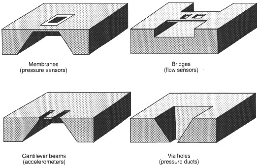
FIGURE 2-1 Three-dimensional configurations that can be produced by combining directionally dependent and impurity dependent etching with photolithographic patterning.
that patterned features must be spaced relatively far apart so that adjacent features do not merge by the lateral etching of the features. Also because of lateral pattern etching, the features on the mask and pattern transfer layer must be biased or reduced (and sometimes even distorted) to achieve the desired feature size and shape at the completion of the etch process. Thus, complex curved patterns and closely spaced structures-closer than a few micrometers-are very difficult to make using wet-chemical etching.
Bulk micromachining process technology is currently undergoing a revolution driven by the incorporation of deep reactive-ion-etching (DRIE) of silicon as a replacement for orientation-dependent (wet) etching. The traditional wet etches limit the range of structures, shapes, and minimum geometries because they rely on the crystallographic orientation of the wafer. DRIE eliminates many of these restrictions, allowing 90-degree sidewall angles (which reduces device size) and randomly shaped linear geometries (Figures 2-2 and 2-3). The DRIE process can also produce structures with high-aspect-ratios similar to those produced by LIGA.
DRIE bulk micromachining can be implemented in many ways, from single wafer, diaphragm, or structured devices, to more complex bonded wafer structures. An example of a bonded wafer accelerometer structure is illustrated in Figure 2-2. The bottom wafer can either be patterned by traditional wet etching methods (a) or can have an oxide defined region that will later be removed by sacrificial etching. A second silicon wafer is bonded to the bottom wafer (b, c) creating either an enclosed cavity or an enclosed oxide region. Lithographic patterning and DRIE are performed on the surface of the top wafer, defining the structural components on the accelerometer (d, e). If the buried oxide method is used, the oxide is then removed by sacrificial etching. Using DRIE in this manner allows the development of non-orthogonal, complex shapes (Figure 2-3). This method can also be used with
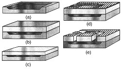
FIGURE 2-2 Generalized process flow for silicon fusion bonding and deep reactive-ion etching (DRIE). (a) A cavity is etched in the bottom wafer. (b) A second wafer is fusion bonded onto the bottom wafer, forming buried cavities. Wafer bonding is also possible with an intermediate oxide to provide electrical isolation. (c) The top wafer is polished down to the desired final thickness. This can also be done by various types of electrochemical etching steps. (d) The metallization and patterning is done along with the DRIE masking and patterning. (e) The DRIE etch through the top wafer into the buried cavity releases the microstructures. Source: Klaassen et al., 1995.
other devices and wafer stacks to produce an entirely new class of bulk micromachined silicon devices.
Controlling the etching of films and bulk silicon needs further study. Since the fabrication of three-dimensional structures is almost intrinsic in the world of integrated MEMS, etching in a controlled fashion and tailoring the isotropic or anisotropic etch-rates of various materials is desirable. Methods and processes to integrate electrically and/or thermally isolated segments of the suspended microstructures are also important for making MEMS.
Bulk Micromachining for MEMS with Electronics
Bulk micromachining with integrated electronics makes use of the mechanical, electronic, and thermal-oxidation (silicon dioxide) properties of single-crystal silicon. Additional advantages of bulk micromachining with electronics include the ability to fabricate suspended, very-high-aspect-ratio (100:1) structures over a large area and the partitioning of the major portion of the electronics off-chip.
One approach to the bulk micromachining of devices with electronics is to partition the silicon chip area to separate the MEMS from the electronics. The electronics area is fabricated first using standard multiple mask-level silicon processing, reserving and protecting selected areas for the MEMS. Subsequent processing sequences are then used to fabricate the MEMS (Figure 2-3). The bulk micromachining steps are usually used to protect the completed electronics during the

FIGURE 2-3 Torsional MEMS structure made possible by DRIE bulk micromachining processes. Source: NovaSensor.
wet-chemical etching or RIE of selected areas, as described in the previous section. Ionic contamination, surface charging, and elevated temperature cycling can affect the operation and ultimate stability of the electronic devices. RIE-based processes, which do not require high-temperatures and do not expose the wafers to ionic contamination, allow the fabrication of single-crystal silicon structures with structure spacings limited only by the lithography and pattern-transfer processes.
Although bulk micromachining techniques allow for transistors and interconnect elements to be integrated on suspended or isolated silicon structures, it is generally only possible to produce the electronics before performing bulk etching for mechanical structures. Key challenges for post transistor micromachining include protection of the electronics from wet-chemical attack, planarization of the wafer surface before initiating the micromachining, and the inclusion of nonstandard MEMS processes and materials. The addition of materials that are not IC-compatible usually requires that the MEMS be fabricated after completion of the IC processing.
Another approach is to integrate the electronic and micromachining process steps. The advantage of this approach is that electronic devices can be integrated on complex suspended and moving structures to provide local power, amplification, impedance matching, and switching. In addition, integrated electronics with MEMS processing can minimize the complexity of the on-chip electronics for specific applications and may make it possible to partition the major electronic functions off-chip, allowing the use of standard electronic chips or application specific ICs (ASICS) for signal processing and control.
Thin bulk-micromachined, single-crystal silicon structures with integrated electronics can also be made using the ''dissolved-wafer process" (Najafi and Wise, 1986). An example of a device fabricated with this process is a multichannel neural probe with integrated electronics (Figure 2-4). In this process a boron etch-stop is used to terminate a back-side etch below the micromachined structures and electronics integrated on the wafer top side.
The challenges of bulk micromachining with electronics include the need for DRIE and/or wet-chemical etching of silicon; the need to protect prefabricated microelectronics from subsequent micromachining steps; and the possible need to planarize the wafer surface via thick photoresist steps and/or chemical-mechanical polishing. The recent introduction of high etch-rate (> 2µm/min) inductively coupled plasma (ICP) tools has generated renewed interest in bulk micromachining with integrated electronics. The introduction of high etch-rate ICP tools in semiconductor laboratories makes the cost structure of RIE etching less prohibitive as an alternative to surface micromachining.
The challenges of DRIE processes include: controlling the isotropic undercut etch; designing the microstructures so that they can be thermally isolated without distortion; increasing
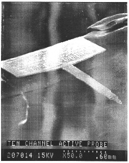
FIGURE 2-4 Multichannel neural probe with integrated electronics fabricated by the dissolved-wafer process. Source: Najafi and Wise, 1986.
the etch rate above 3µm/min and/or increasing the production throughput using multiple-wafer DRIE tools; developing conformal deposition processes that deposit uniform layers of ceramics and metals on the sidewalls of the high-aspect-ratio processes; developing low-temperature deposition processes compatible with deposition on completed ICs; and developing multiple level bulk micromachining processes.
Surface Micromachining Processes
Surface micromachining makes use of traditional microelectronics fabrication techniques to create mechanical systems with micron-sized features. In contrast to bulk micromachining, which forms structures by etching into the bulk of the wafer, the hallmark of surface micromachining is that mechanical features are etched into thin-films that have been deposited on the surface of silicon wafers. The surface micromachining method can use any of several materials as the mechanical layer with variations serving as the sacrificial layer. Most often, polycrystalline silicon is used for the mechanical layer and silicon dioxide is used for the sacrificial layer because these materials are the most easily adapted from
the materials available in the IC field and their fabrication techniques permit the simultaneous fabrication of thousands or tens of thousands of mechanical structures across the surface of the wafer.
A typical polysilicon-based process begins by depositing a thin-film (¬0.5 to 2.0 µm) of a sacrificial material onto the surface of the wafer. A common sacrificial material is a chemically vapor-deposited (CVD) oxide. Traditional photolithography and dry-etch processes are then used to cut holes at selected sites through the sacrificial layer to the silicon surface. These holes serve as the anchor sites for the structural material to contact the underlying wafer. The thin-film of structural material is then deposited, patterned, and etched to form the micromechanical structures. The fabrication sequence is completed with the immersion of the wafer in hydrofluoric acid, the etch rate of which is very different for polycrystalline silicon than for silicon dioxide. This highly selective release-etch removes the silicon dioxide and leaves the polycrystalline silicon structures suspended above the wafer surface everywhere except where the anchor cuts were made.
Surface micromachining techniques have been used to create a variety of sensors and actuators, including accelerometers, gyros, pressure sensors, combustible-gas sensors, and a variety of resonant structures. Many of these devices are now in commercial applications, especially accelerometers. Devices fabricated using surface micromachining use similar process-control and batch-fabrication techniques to those developed for the IC-industry. Using these well established techniques enables the batch fabrication of low-cost, high-performance MEMS. Because the nominal thickness of the polycrystalline silicon layer is 2 µm, however, the out-of plane stiffness usually limits the suspension span of the microstructures and devices to a few hundred micrometers. The structure release and drying steps also limit the maximum size of the suspended microstructures.
An important challenge in surface micromachining fabrication comes at the end of the fabrication sequence, however, during the final rinsing and drying of the wafers. After the sacrificial material has been removed and during the final drying process, a meniscus forms between the bottom of a suspended mechanical structure and the surface of the wafer. As the water dries, the meniscus pulls the suspended mechanical structures toward the surface, and the structures become stuck together. A similar meniscus can form between adjacent mechanical structures, causing them to stick together. This phenomenon is known as stiction.
A low-cost manufacturable technology requires that the problem of stiction be overcome. Several techniques have been developed to circumvent the problem. First, design techniques have been used to minimize stiction by limiting the area of contact between suspended structures and the substrate. One way to accomplish this is to etch regularly spaced dimple cuts into the sacrificial layer before the deposition of the structural material. Unlike the anchor cut, the dimple cut does not perforate the entire sacrificial oxide layer. When the structural material is then deposited onto the sacrificial layer, the material conforms to the dimples in the sacrificial layer, and small bumps are formed along the bottom of the structural material. These bumps limit the contact area between the suspended structures and the substrate and mitigate the stiction problem.
Several promising process techniques have also been developed for reducing or eliminating stiction. For example, the meniscus problem can be completely eliminated by utilizing a supercritical CO2 drying technique in which the sacrificial release-etchant is displaced with water and then with methanol. The wafers are then placed in a pressure chamber where liquid CO2 is introduced to displace the methanol. The temperature is raised to transform the liquid CO2 to a supercritical fluid, after which the pressure is dropped, returning the supercritical fluid to a gaseous state. Thus the liquid-to-gas transition interface that creates the meniscus problem is completely avoided. This CO2 technique has been used to release structures that are millimeters in size and has enabled the high-yield manufacture of complex surface micromachined MEMS. Supercritical CO2 drying is a standard process in the food-processing industry and is an excellent example of how existing industrial manufacturing techniques can be adopted by the MEMS industry.
A related technique to avoid the formation of a meniscus is the freeze-sublimation technique in which the release-etchant is displaced by water and then by an organic solvent with a high freezing temperature. The wafer with solvent is cooled until the solvent is frozen. The pressure is then dropped to vacuum levels, and the frozen solvent sublimes. This technique is analogous to the common food-processing technique of freeze drying. Another way to avoid stiction is to make the surface hydrophobic by coating it with ammonium ions.
The techniques described above avoid stiction during drying, but stiction can still be a problem during the operation of actuated MEMS. If shock, electrostatic discharge, or some other stimulus causes individual MEMS components to touch either each other or the substrate, they may become stuck. In these cases, surface treatments are needed to change the energy state, or "stickiness," of the surfaces. Promising results from treatments with amoniafloride have been demonstrated, and work with several self-assembling monolayers have shown promising results at the early research stage in reducing both stiction and friction (Houston, Maboudian, and Howe, 1995). The development of manufacturable low-stiction surface modifications for the commonly used surface micromachining materials is a major area of investigation.
Surface Micromachining to Produce Multilevel MEMS
Dramatic increases in mechanical complexity and functionality can be achieved with surface micromachining
technologies that incorporate two or more levels of polysilicon. Continued extension of the technology enables the fabrication of mechanically complex systems, including motors, tools, and the interconnections to couple them. Fabricating micromachines with three or more levels of structural polysilicon requires more than a logical extension of simpler technologies, however. Almost all microelectronic fabrication tools were designed to work with near-planar surfaces. As micromachines are formed on the surface of the wafer, nonplanarity and significant nonplanar topography begin to develop. Each additional level of polysilicon complicates the topography problem. The sacrificial layer that is placed on top of a structural level of polysilicon conforms to the shape of that layer. When another layer of polysilicon is deposited, it is not flat, so the structural details of the first level are, in effect, imprinted on the upper level. This problem is compounded with each level of polysilicon. The problem can result in the presence of untenable stringers, alignment difficulties, and unintended structures that can interfere with the proper operation of the micromachine. Topography problems complicate the development of surface micromachining technologies that have three or more levels of polysilicon.
The established IC-fabrication technique of chemical-mechanical polishing (CMP) may be able to overcome topography problems in multilevel polysilicon technologies. Using CMP, wafers are polished flat after each sacrificial-oxide deposition, which results in perfect planarity of each structural level and eliminates the stringer and mechanical parasitic problems. MEMS have been built with five levels of polysilicon using the CMP technique.
Surface micromachining has matured sufficiently to give rise to foundry services. MCNC, under DARPA sponsorship, offers a very inexpensive foundry service for surface micromachining. The technology offers two structural levels of polysilicon and an additional level of polycrystalline silicon for electrical interconnection. A broad variety of researchers have made use of this service to create both simple and complex structured MEMS.
Surface micromachining technologies can also be used on material systems other than structural polysilicon and sacrificial layers of silicon dioxide. For example, TI uses a photoresist as the sacrificial layer and aluminum as the structural material in their DMD (Hornbeck, 1995). There are several important considerations in choosing combinations of materials for surface micromachining, however. First, to create fully released structures, sacrificial and structural materials must be chosen that react to some highly selective etchant. Second, the ability to deposit the structural material in a low-stress state or to achieve a low-stress state through a thermal anneal is critical to prevent curling of the mechanical parts when they are released. If high-temperature anneals for stress reduction are needed, the underlying sacrificial layers must be able to withstand the treatments. Another consideration is the advantages of using well known and accepted microelectronic materials.
CLASSIFYING INTEGRATED CIRCUIT-BASED TECHNOLOGIES
The objective of this section is to classify the IC-based technologies that have been or might be useful for the manufacture of MEMS. The classification can be of value in assessing the cost/benefit ratios of a proposed MEMS process and in stimulating thought about new directions for MEMS.
From the IC experience, it is clear that innovation in either materials or procedures exacts a cost, and every innovation must be evaluated in terms of a cost/benefit analysis. The degrees of innovation are not readily quantifiable; they are defined on the basis of MEMS experience and an understanding of the steps in the IC process. Fuzzy definitions are regrettable but probably unavoidable. For example, from one perspective, the polysilicon used for substrate micromachining differs substantially (in terms of its deposition procedures, dimensions, and physical properties) from the polysilicon made for electronics use in ICs and could be classified as a new material.1 This distinction will not be made in the following sections. Polysilicon will be treated as an old material.
MEMS production processes will be characterized in the following sections in terms of two sets of variables: (1) the materials being processed and (2) the processing steps and equipment (tools). Innovation in either set will generally incur "startup costs" in terms of money, time delays, and/or extra work for qualification purposes. As an example, polysilicon surface micromachining, described earlier in this chapter, is carried out using materials that are well known in IC manufacture (old materials) and with IC process steps that are also well known (old tools). If the surface micromachining process were to be complicated by moving to more than three layers of structural polysilicon, a CMP step would probably have to be added, which can be considered a new tool and would add a level of complication to the process.
MEMS with Old Materials and Old Tools
MEMS that use only those IC processes now in use for integrated microelectronics are most acceptable to the existing manufacturing capabilities. Some MEMS have been successfully made this way (usually with a few added post-IC-process steps). The design space is severely limited,
however, and the designer must account for relatively uncontrolled mechanical properties in the structures.
Many years of experience in the production of silicon diaphragm pressure sensors clearly qualifies their production processes as old tools. However, when they were first introduced in the 1960s, anisotropic wet-etching and etch stopping with highly doped boron layers would have been new tools. The subsequent development of nozzles for silicon ink-jets using anisotropic etching was aided by experience with the diaphragm pressure sensor. As this example shows, the number of tools in this first classification of MEMS processes grows as mastery of once-new materials and technologies grows.
Cleverness is the important parameter that can lead to advances in this category. A clever MEMS engineer should reconsider older processes that are only occasionally (or no longer) used and capitalize on established know-how if resurrecting them should prove worthwhile. Many of the MEMS technologies in this category are product-specific, however. For example, two of the most advanced MEMS products are TI's DMD and Analog Device's integrated accelerometer.
Both products leverage existing microelectronics fabrication techniques but utilize different structural and sacrificial materials. Consequently, solving manufacturing problems for one would not necessarily solve problems for the other.
MEMS with Old Materials and New Tools
New tools in the MEMS area have traditionally been qualified through their use in specialized areas-often in a selected region of the IC world. An example that appears to have many MEMS applications is DRIE, a process that was developed to open a third dimension in IC semiconductor-memory applications. As described earlier in this chapter, bulk-silicon microstructures have historically been produced through the use of wet-chemical etchants. Although wet-etching techniques are well established, they have a number of drawbacks, including the inability to achieve vertical-sidewalls and non-orthogonal linear geometries in <100> silicon and the reaction of wet chemicals with films on the wafer surface. A capability to produce high-aspect-ratio, vertical-sidewall features in silicon is being provided using DRIE techniques and several recent commercial systems. Significant reductions in device area can be realized by changing the etch sidewall angle from 54.7 degrees to ¬90 degrees for devices that use back-side etching to produce or release front-side structures. This technology has applications in all areas of traditional bulk micromachining, such as pressure sensors, fluidic microstructures, and accelerometers. An example of an inventive use of DRIE is for the process called HEXSIL (combining HEXagonal honeycomb geometries for making rigid structures with thin-films and SILicon). HEXSIL (discussed further in Chapter 3) combines surface micromachining with DRIE trenches in silicon (Keller and Ferrari, 1994). Although DRIE has provided new options and opportunities, it still presents a number of challenges. First, although at present DRIE provides the capability of etching a few hundreds of microns into (or through) a silicon wafer, the silicon etch-rate is dependent upon the width of the exposed silicon feature, which leads to varying etch depths as a function of feature size (Figure 2-5). Work needs to continue either to eliminate the etch-rate dependency or to develop design and processing rules to correct for it. DRIE would then be applicable to the broadest class of structures. Second, although the silicon etch-rate has increased by orders of magnitude over the rate for earlier generations of silicon RIE machines, the current rate is only microns per minute. This rate might be tolerable if the equipment were capable of batch-wafer processing, but current and near-term equipment is suitable only for single-wafer processing. To use DRIE in a process that requires more than 100 microns of etching would necessitate installing systems with multiple etch-chambers to maintain a production schedule. Third, the DRIE process may be well suited for silicon materials, but it is generally not appropriate at this time for other materials (e.g., dielectrics, metals, or ceramics). The importance of extending DRIE to nonsilicon materials is becoming increasingly apparent, however, as microfluidic applications for MEMS grow in importance. Configured fluid channels and devices in glass, plastics, ceramics, and metals warrant developing DRIE methods for processing them.
MEMS with New Materials and Old Tools
The category of new materials and old tools is very important for emerging technologies because it does not require significant capital investment. Ideally new materials would
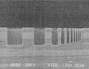
FIGURE 2-5 Deep reactive-ion etching (DRIE) depth as a function of feature width. Features shown are 2 to 50 microns wide. Source: MCNC MEMS Technology Applications Center.
be introduced as thin-films and could be used with processes and equipment familiar to the IC world (e.g., low-pressure chemical-vapor deposition [LPCVD] or, less favorably, sputtering). Similarly, CVD processes in standard CVD equipment could be used with temperature and flow changes to make familiar materials with new properties. Low-stress silicon nitride is a material that could fall into this classification. It is generally deposited in the same LPCVD tubes that historically have produced stoichiometric silicon nitride but with significantly different gas flows and pressures. Efforts are also under way to incorporate materials with useful properties for sensing and actuation, such as ferroelectrics, piezoelectrics, and magnetic films, into MEMS processes (see Chapter 3).
The selective deposition of materials on patterned substrates is common in ICs and will increase as new materials are introduced. The selective deposition techniques for silicon and metals (e.g., tungsten) used in IC processes could find their way into MEMS processing over time. The ways, means, and materials suitable for this whole family of techniques require significantly more fundamental research, however.
MEMS with New Materials and New Tools
The combination of new materials and new tools presents formidable challenges, and progress will probably be slowest in this category. This should not, however, rule out the consideration of this class of MEMS research, but the benefits should be compelling (see Chapter 3). The "newness" of either materials or tools can vary considerably because some materials and tools previously used for special purposes may provide sufficient basic knowledge for them to be transferred easily to the MEMS area. For example, electroplated magnetic materials and processes are familiar from their use in the magnetic memory storage area. If the manufacturing issues specific to micromechanical materials can be successfully addressed, these materials and tool sets may move from being the most difficult to the least difficult to incorporate. Nevertheless, the application of electroplating will require improved facilities and extensive characterization before the full potential of this technique can be realized.
SUMMARY
The enthusiasm for and promise of MEMS has, to a large extent, arisen from the demonstrated ability to produce three-dimensional fixed or moving mechanical structures using lithography-based processing techniques derived from the established IC field. Conventional IC materials can be used innovatively in MEMS, and much of the needed MEMS-specific hardware can still be leveraged from IC-technology. These MEMS developments are most likely to be accepted in traditional IC fabrication facilities and are, therefore, most likely to succeed commercially.
There are many opportunities for creative work in MEMS based on what is already known about IC processing, particularly in re-evaluating the range of knowledge compiled during the history of IC development. MEMS products that rely on conventional IC tools, materials, processes, and fabrication techniques have the highest probability of achieving the same manufacturability, performance, low cost, and high reliability as in the production of modern VLSI circuits.
At the heart of MEMS development is the ability to construct extremely small mechanical devices, preferably using batch processing. Wet etching has historically dominated the MEMS field because (1) three-dimensional structures can be micromachined from substrate silicon and (2) chemical-etch equipment is well established, simple, and inexpensive. The disadvantages of wet-chemical processing are its inability to achieve vertical-sidewalls and non-orthogonal linear geometries in <100> silicon and its reaction with films on the wafer surface. Although dry etching is a mainstay of IC processing and gas-phase "dry" etching techniques are currently being investigated for MEMS production, the film thicknesses or substrate-etch depths for MEMS are often significantly greater than for IC fabrication. Therefore, MEMS etching will typically present additional challenges. If only IC-based techniques are used, it will limit the number of applications that can be pursued. As will be seen in the next chapter, flexibility may open broad new areas for MEMS, although problems with manufacturability and reliability should be anticipated in the early stages.
Conclusion. The expertise and advanced state of the current microelectronics industry provides an enormous advantage for the development of MEMS. Leveraging and extending existing IC tools, materials, processes, and fabrication techniques are excellent strategies for producing MEMS with comparable levels of manufacturability, performance, cost, and reliability to those of modern VLSI circuits. Because controlled etching is so important to the fabrication of three-dimensional structures and the progress of MEMS, improving etching methods, including those that tailor isotropic or anisotropic etch-rates of various materials, will be important.
Recommendation. Efforts to identify solutions to the challenges of producing MEMS should capitalize on relatively well understood and well documented IC materials and processes. Solutions may be found in current IC practices but may also result from creatively re-establishing older IC technologies.
Recommendation. Further research and development should be undertaken to improve etches, etching, and etching controls for MEMS. This work should take into account the realities and limitations of manufacturing process equipment.


