
3
New Materials and Processes
The previous chapter discussed the application of conventional IC tools, materials, processes, and fabrication techniques to MEMS. This chapter focuses on the rationale and requirements for the introduction of new materials and processes that can extend the capabilities and applications of MEMS and that are reasonably compatible with IC-based, batch-fabrication processes. The chapter begins by considering the motivations for introducing new materials and processes. Overviews are then presented of the materials and processes required to produce high-aspect-ratio structures, enhanced-forced microactuation, improved environmental resistance, enhanced surfaces, and improved power supplies.
MOTIVATIONS FOR NEW TECHNOLOGIES
At least five factors motivate the development of MEMS technologies beyond the ones that rely on conventional IC tools and materials. First, some IC-based MEMS are not adequate in applications that require forces commensurate to those in the macroworld. The principal techniques for applying force in IC-based MEMS rely on electrostatic or thermal expansion prime movers, which produce relatively small forces and limited interaction lengths. Materials other than those available in the typical silicon IC complement will have to be integrated into MEMS to make use of physical prime movers that are potentially capable of delivering higher forces or greater interaction lengths.
The second factor favoring the use of nonconventional IC techniques is the need for high-aspect-ratio structures. In the case of surface micromachining, for example, typical mechanical structures are produced with vertical dimensions limited to a few micrometers. Although a process has been developed to produce "pop-up" elements for applications such as photonic devices (Pister et al., 1992), folded-out polysilicon structures are not suitable for all high-aspect-ratio applications.
The third factor is the need for materials that can operate in severe environments. MEMS applications for chemical analysis, fluid control, and other purposes have been clearly identified in the automotive, electrical, defense, and nuclear industries. These applications, however, demand operation in high-temperature, corrosive environments (e.g., car engines, auto tires, nuclear reactors, chemical process-control facilities, or ordnance).
The fourth factor is the importance of surface effects in many MEMS devices. For example, in chemical- and biochemical-sensor applications, there must be very limited or no interaction between an analyte and the exposed contact surfaces. Methods for modifying and coating the surfaces of exposed devices in MEMS are required to prevent interactions. Solid-solid interface sticking (stiction) might also be mitigated by new materials and processes.
The fifth factor is enlarging the design space for MEMS. This concept is controversial within the MEMS community and has been the subject of considerable debate, which usually centers on the "good versus evil" of standardized processes. Proponents of standardization claim that it is essential for the growth of the industry because it provides a stable, repeatable technology base that can be supported by design rules, distributed CAD support, and the economic yield from many different products. Years of experience in the IC industry have indicated that there is no such thing as a small change in an IC-fabrication process. Changes invariably introduce unforeseen problems. Thus, if new materials or processes are added to a conventional IC process to support MEMS production, they should be added at the back end, preferably off line, in a dedicated process area.
Opponents of standardization are concerned that it will stifle growth while the field is still very young and may exclude some potentially important developments. A similar controversy arose during the early years of IC development, and relative standardization of processes and materials occurred only after more than a decade of commercial production. The IC experience constitutes a prehistory for MEMS, but its consequences in terms of infrastructure provide a strong influence that tends to inhibit the introduction of new materials and processes unless they are shown to be absolutely necessary.
MATERIALS AND PROCESSES FOR HIGH-ASPECT-RATIO STRUCTURES
A serious challenge facing the development and application of MEMS is the production of parts with the structured dimensionally to interface with and affect the macroworld.
This section focuses on two processes that can produce high aspect ratio (> 100:1), batch-fabricated components that can be integrated with IC-based wafer processing: HEXSIL and LIGA (Lithographie, Galvanoformung, Abformung).
HEXSIL
The HEXSIL method of producing high-aspect-ratio parts (mentioned in the taxonomy section of Chapter 2) involves a combination of DRIE and surface micromachining techniques. HEXSIL combines HEXagonal honeycomb geometries for making rigid structures with thin-films and SILicon for surface micromachining and CMOS electronics. The trenches serve as reusable molds that can be sequentially filled with polysilicon and sacrificial layers of oxide. After patterning and the removal of sacrificial layers, structural members with large lateral dimensions (ranging up to centimeters) can be formed from arrays of polysilicon honeycombs. Thus, through the HEXSIL process, batch processing of thin-film layers can be used to produce elements that form a transition between the millimeter and micrometer worlds.
An example of HEXSIL is a pair of tweezers that can pick up particles ranging roughly from 1 to 25 µm and place them on platforms (also made of HEXSIL) under operator control (Figure 3-1; Keller and Howe, 1997). This basic process has also been combined with nickel plating to produce highly conducting regions on the HEXSIL plates for contacts and conducting patterns. Thermal expansion of resistively heated HEXSIL regions has been used to actuate HEXSIL structures, such as the tweezers. Using interconnected levers, the very tiny expansion in polysilicon beams can be multiplied to produce multiple millimeters of motion (Keller and Howe, 1995).
The HEXSIL process is an interesting example of the way high-cost machines and processes (e.g., DRIE) can support a major leap forward in MEMS. The development costs for trench etchers were paid by IC producers who saw ways to increase the density of semiconductor-memory arrays by adding a third dimension on the chip. For MEMS, DRIE etchers promise nearer-term, silicon-compatible processing of high-aspect-ratio structures. As this promise becomes a reality, MEMS-specific DRIE machines can be expected to evolve. By the same reasoning, fine-structured, nonplanar metal-film plating apparatus and techniques for reliable deep trench film coating and etching will also be mastered. Because HEXSIL currently uses IC-based technologies, compatibility with these technologies is not an issue. An important area of research required to make HEXSIL a designable and versatile MEMS process, however, is the establishment of the basic mechanical properties (e.g., internal stress, Young's modulus, fatigue strength) of polysilicon so that it can be qualified for new applications.
LIGA
Small, precision-metal components have historically been produced by serial methods, such as computer numerical controlled (CNC) milling or micro-electron discharge machining (micro-EDM). Although serial methods are capable of producing high-precision parts in a variety of metals, they can result in high per-piece costs or part-to-part variations. To drive down the cost of high-precision parts to a level supportable by general systems use, batch-fabrication methods need to be developed.
LIGA (Becker et al., 1986) was developed at the German nuclear research center, the Kernforschungszentrum Karlsruhe, for the production of high-precision, high-aspect-ratio parts in a batch-processing environment. LIGA utilizes x-ray exposure of a resist film, typically polymethylmethacrylate (PMMA), followed by electroplating into the template produced by the exposure to yield a primary metal part. This metal part can be either the final device or, if multiple plastic or metal copies are desired, the master for an injection mold. Figure 3-2 illustrates a basic LIGA process. Figure 3-3 shows metal and plastic parts produced using LIGA.
The LIGA method generally uses nickel or permalloy (NiFe) as the electro deposited material. Subsequent injection molding usually uses plastics. Multilevel LIGA enables fabrication of components from more than one material or material type for bimorphic applications or friction and wear reduction.
Using multilevel exposure techniques in LIGA processing, which was demonstrated recently (Guckel et al., 1996b), provides for the formation of complex structures, the integration of multiple material layers, and some degree of batch assembly. Multilevel LIGA has a number of added processing requirements, including planarization of the sequentially electroplated layers, adhesion of PMMA to the planarized levels, alignment of the layers, and electroplating of multiple layers.
Compatibility and Manufacturing Constraints of LIGA
The compatibility of LIGA and silicon processing (IC and MEMS) was demonstrated by Guckel et al. (1989), who produced photodiodes in the silicon substrate as part of a motor-position sensing system, and by the HI-MEMS Alliance in the development of a hydrostat that directly integrates LIGA with bulk micromachining (Egert and Felde, 1995).
Researchers have successfully demonstrated the utility of LIGA for the production of prototype metal and plastic precision parts, but the transition of LIGA into manufacturing level processes has been slow. A number of issues and challenges still face LIGA before it can be accepted and integrated into a manufacturing environment. Although some
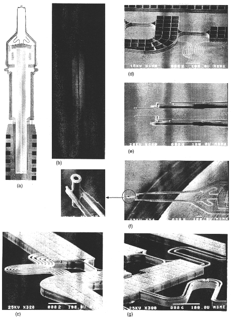
FIGURE 3-1 Photomicrographs of HEXSIL tweezers: (a) HEXSIL tweezers design; (b) center of actuator heated to incandescence; (c) surface polyflex cable for interconnects between rotating rigid HEXSIL beams; (d) bottom view of 45 µm high honeycomb structure of rigid beams; (e) compliant surface polysilicon tips built on HEXSIL foundation; (f) transition from micro- to milli-scale beams provides mechanical interface; (g) semicircular beam with full Wheatstone bridge for position sensing. Source: Keller and Howe, 1997.
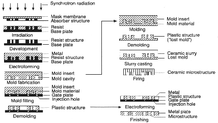
FIGURE 3-2 Schematic illustration of the steps involved in the basic LIGA process. Source: Ehrfeld and Lehr, 1995.
commercialization drivers are being addressed both in the United States (the HI-MEMS Alliance [MCNC] and MEMSTek) and in Germany (Microparts), the adaptation of LIGA into a high-volume manufacturing environment appears to be years away.
Using LIGA in the production of large quantities of high-precision parts is hampered by several throughput constraints. Although all the process steps involved in LIGA are batchor wafer-level procedures, limitations persist in the following areas: applying the PMMA onto the wafer, the exposure of large numbers of wafers (if replication is not being used), electroplating and "finishing" the primary templates, and using methods like injection molding, hot embossing, and casting for mass replication. There are two major approaches
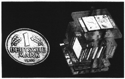
FIGURE 3-3 Metal and plastic parts produced using LIGA. Source: Forschungszentrum Karlsruhe GmbH, Germany.
for improving throughput for LIGA. Most activity in the United States is focused on improving the exposure throughput to allow large volumes of primary template wafers to be produced and eliminate the need for replication. In Germany, the use of replication techniques has been heavily pursued.
One reason for the two approaches is the availability of high-energy x-ray source laboratories in the United States (e.g., the National Synchrotron Light Source, the Stanford Synchrotron Radiation Laboratory, and the Advanced Photon Source), which allows simultaneous exposure of large numbers of PMMA template substrates.
The primary method of PMMA application is solvent bonding of a prefabricated sheet of low-strain material (Skrobis, Taylor, and Engelstad, 1995; Guckel, 1996), which minimizes the problem of high-strain fields in the PMMA. This method utilizes preforms cut from commercially supplied PMMA, which are attached to the substrate by a spun adhesion layer. The PMMA is then milled to the desired thickness. At present, this process is labor intensive and limits the throughput. Other methods of PMMA application have also been explored (Mohr, Ehrfeld, and Munchmeyer, 1988), as well as alternative materials for templates (polyimides). Because of the residual strain in the material, the utility of these methods is limited to tens of microns in thickness, however.
The total thickness of PMMA exposed is a function of the usable x-ray flux transmitted through the mask. The flux delivered for most synchrotrons at the wafer surface after the soft x-rays are filtered out is sufficient for only one PMMA layer of 500 µm or less per hour. To improve the exposure throughput, highly energetic sources (e.g., the National
Synchrotron Light Source) are used, increasing the exposure throughput by an order of magnitude or more.
Although electroplating of metals like nickel, copper, and permalloy have become mainstream manufacturing processes in the disk-drive industry, electroplating large numbers of wafers containing small, high-aspect-ratio structures has not. Transporting plating reactants into 500 µm deep, 20 µm wide features stresses the state of the art in single-wafer and batch-electroplating systems. Another challenge is performing deep plating over a wafer surface with a variable plating area.
Ultimately, the utility of LIGA for commodity, mass-produced parts will probably be enhanced by the use of traditional replication methods, such as injection molding, embossing, and casting. Although throughput using these techniques is well known in the macro (millimeter and greater) domain, the problems of using them for microfabricated parts are not well understood. A significant effort is under way in Germany to implement mass replication techniques via modifications of existing production-molding equipment (Becker et al., 1986). Efforts have been hampered by a number of problems, including handling of the mold masters, injection- or embossing-pressure management, flow dynamics in the dimensions of LIGA molds, mold release, and mold lifetime.
Whether LIGA systems are produced by replication or batch-exposure methods, they generally require further assembly of multiple, submillimeter components. In fact, this microassembly requirement will probably determine whether or not the LIGA process is viable. Self-assembly techniques have been demonstrated in surface micromachining (Chapter 2), but they have not yet been demonstrated for LIGA, which is characterized by assembled tolerances of less than 1 µm.
Ongoing research is addressing many of the technical issues connected with LIGA. For example, the disk-drive industry has undertaken extensive research in batch-electroplating techniques that may be applicable to LIGA. A final challenge that LIGA must overcome is the synchrotron scare factor. Many companies are wary of processes that rely upon equipment they cannot install in their own factories or that is located at a government or university facility with a "questionable" commitment to commercial manufacturing (Markus et al., 1996). The scare factor will not be overcome until several successful commercial products have been demonstrated and supported.
MATERIALS AND PROCESSES FOR ENHANCED-FORCE MICROACTUATION
Microscale devices can be actuated by a variety of mechanisms. An important challenge for many MEMS applications, however, is to make microactuators that can deliver sizable forces and in some cases large displacements. In this section, mechanisms that can be implemented using thin-film materials are briefly discussed, including magnetic, piezoelectric, electrostrictive, magnetostrictive, and shape-memory alloy materials.
Materials
Magnetic Thin-Films
MEMS researchers are using magnetic materials primarily for the development of high-torque/high-force actuators. Torques of 10-5 Nm for rotational magnetic microactuators (Guckel et al., 1996a) and forces reaching to the mN range with displacements of 250 µm for linear actuators have been reported (Rogge et al., 1996). Actuating a magnetic element using an off-chip source provides a significant advantage in some MEMS designs (Sniegowski et al., 1996). Other concepts for MEMS in which a strong local magnetic field would be useful have been inhibited by the difficulty of supplying that field at the current levels available in ICs.
Most magnetic thin-film materials in MEMS are deposited by electroplating, which has been refined as a result of many years of experience in the large-scale commercial data-disk storage industry (e.g., Ahn et al., 1996). Films are typically nickel or alloys of nickel and iron. Techniques for integrating magnetic thin-films with an IC process have also been demonstrated (Guckel et al., 1993; Judy and Muller, 1996). Some results with sputtered films have also been reported (Yamashita et al., 1991), and both low-permeability nickel and high-permeability non-nickel alloys have been patterned into complex geometries with high-aspect-ratios using the LIGA process (Guckel et al., 1994).
The promising results thus far make it likely that magnetic films will be added to IC-derived processes for MEMS, at least in some facilities. The progress made in research must still be qualified for commercial applications by demonstrating reliable long-term compatibility in an overall MEMS process.
Piezoelectric Films
Most large-force, large-deflection actuation materials are ferroic ceramics or metals with complex domain structures that are poised on an instability to give a large mechanical response to external fields or forces. Piezoelectric actuators made from ferroelectric PZT (PbZr1-xTixO3) ceramics are the most widely used electromechanical transducers for sensing and actuating in larger-scale devices. In these materials, force and electric field are proportional. PZT films have been successfully laid down on silicon by sol-gel and vapor-phase methods.
Multilayer ceramic actuators are manufactured worldwide for use as micropositioners, printers, micromotors, vibration
suppressers, hydraulic valves, automotive fuel injectors, and switches. But the fabrication of these devices is not directly compatible with silicon IC-process technology.
The significant increase in force achievable with piezoelectric materials, however, has sparked considerable interest in methods for integrating PZT films directly into silicon MEMS processes. To illustrate the capability of materials, consider a microactuator with parallel electrodes 10 m apart and an electrode area of 100 mm2. The force for an electrostatic actuator with an air gap between the electrodes is given by the Maxwell stress, s:
Felectrostatic= sA = -1/2 AKaire0E
(1)
However, with poled PZT between the electrodes the maximum force is:
Fpiezoelectic= sA = Ae33E
(2)
The ratio |FpiezoelectricFelectrostatic| is, therefore:
| Fpiezoelectric/Felecrostatic| = 2e33/Ke0E
(3)
In these expressions A is the electrode area, K is the dielectric constant, e0 is the permitivity of free space, e33 is the piezoelectric stress coefficient (~10 C/m2 for PZT), and E is the electric field. For an electrostatic actuator, Emax is about 3 MV/m, which is the breakdown strength of air. For a piezoelectric ceramic, the depoling field provides a limit at about 3 MV/m, which is on the same order as typical insulator breakdown fields. Therefore, assuming a field of 106 V/m and using Ke0 equal to 3.456 x 10⁻¹¹ F/m for silicon dioxide, Equation (3) predicts a ratio of roughly 6 x 10⁵ for the two forces.
The foregoing example shows that piezoelectric actuators can provide enormous increases in output force compared to those available from electrostatic drives. Although the displacements are not very large for the parallel-plate, piezoelectric-electrode configuration (typically a few nanometers), a PZT-silicon-cantilever design or a flextensional moonie (''bellows") configuration used in macroscopic actuators can greatly amplify the motions by trading force for displacement. Achieving relatively large displacements and high forces simultaneously will probably require more elaborate structures (Zdeblick, 1996).
As MEMS applications proliferate, the ability to apply technologies derived from the multilayer ceramic-actuator field to the integrated, thin-film silicon MEMS field could become very important. Many problems exist, however, from the understanding of basic material properties and processing challenges to integrating these materials into more conventional IC-fabrication methodologies.
Shape-Memory Alloys
A number of intermetallic compounds exhibit a large shape-memory effect in which a deformed metal can be restored to its original ferroelastic shape when heated (Kuribayashi, 1986; Wayman, 1993). This behavior is a consequence of a ferroelastic phase transformation in which the structure changes from the multidomain martensitic state to the higher temperature austenite structure. Obtainable strain for the thermal-memory effect (Ni/Ti and Cu/Zn/Al) is approximately 4.5 percent for bulk material (Wayman, 1993).
Shape-memory structures can have advantages, such as high work-to-mass ratios and noiseless and reliable operation, over conventional actuators. Shape-memory actuators are slow compared to piezoelectrics but offer recoverable strains up to 10 times greater than alternative approaches.
Researchers have attempted to fabricate actuators using thin-film deposited Ni/Ti (NITINOL) as a shape-memory alloy (SMA; Busch, Johnson, and Lee, 1990; Walker, Gabriel, and Mehregany, 1990), but the results to date as to the viability of this approach are not conclusive (Miyazaki, 1990). NITINOL films have been sputtered to thicknesses between 0.2 and 50 µm on a variety of substrates, including silicon. When decoupled from the substrate, some films exhibit shape-recovery characteristics similar to those of bulk NITINOL. The films can be electrically driven using joule heating, and they demonstrate fast cooling rates because of the large surface-to-volume ratio. By selectively etching the shape-memory film and the silicon substrate, SMA microactuators have also been explored for use as electrically driven microvalves. The control of film composition and properties has proven difficult in sputter-deposited films, however, and further study of deposition techniques is needed.
Heat-actuated SMAs are being studied for use in a number of thin-film microdevices (Walker, Gabriel, and Mehregany, 1990). Applications are focused on actuators ranging from microrobotic manipulators to pneumatics for valves in which small TiNi ribbons are stretched to close a silicon-membrane gate. The principal advantages of SMA thin-film actuators are their ability to produce large forces and displacements within small volumes at voltages common in ICs. The availability of thin-film SMA material would greatly aid MEMS applications, but its development has been very slow. Another problem is the necessary local hot region, which can complicate its use in biological applications.
Shape-Memory Polymers
Shape-memory polymers are a relatively recent development (Liang, Rogers, and Malafeew, 1991; Hayashi, Ishikawa, and Jiordana, 1993). They are light, have good shape-recovery characteristics, and may be able to compete with shape-memory alloys in some MEMS applications
(Tobushi et al., 1996). The phase-transition temperature is near to room temperature in many of these materials. Considerable research is required to determine their possible application to MEMS, however.
Magnetostrictive Alloys
Magnetostrictive alloys like TERFENOL-D (Tb1-xDyxFe2) function well as sensors and actuators (Hathaway and Clark, 1993) in the macro scale. A large number of macroscale magnetomechanical transducers and actuators utilizing TERFENOL-D have been designed and manufactured. The high energy density of these actuators, plus their ruggedness and reliability, make them attractive for vibration suppression and high-power sonar. A macroscopic resonant magnetostrictive rotating motor has been reported that can produce a torque of 2 Nm at the low rotating speed of 100 degrees per second (Claeyssen, et al., 1996).
Thin-films of magnetostrictive rare-earth/iron alloys can be sputtered on silicon and patterned by etching or sputtering through masks. Micropump and microvalve membranes and cantilevers are targeted MEMS components (Quandt, Gerlach, and Seemann, 1994), but little has been reported thus far on the incorporation of magnetostrictive materials into an IC-derived process.
Processing
Advances in the use of new materials, novel powder synthesis methods, and ceramic integration are being made in electronic ceramics at scales much greater than those typical of MEMS. Monolithic multifunctional components take advantage of four existing technologies: thick-film methods and materials; multilayer ceramics capacitor processes; cofired package concepts; and thin-film deposition on silicon and other substrates.
Processing Multilayer Ceramics
Improved processing and manufacturing of multilayer ceramics, especially for capacitors and microelectronic packages, has resulted from research on the microstructural property relationships of multilayer ceramics (Herbert, 1985). Fabrication techniques include powder processing, thin-sheet formation, and metallurgical interactions.
Multilayer capacitors and packaging currently make up more than half the electronic ceramics market. Although they cannot be directly integrated with ongoing IC-based MEMS efforts, these technologies can be transferred to the manufacture of multilayer actuators for submillimeter MEMS. More than 29 billion units are manufactured each year for multilayer capacitors and actuators, outnumbering by far any other electronic ceramic component. Multilayer ceramics and hybrid packages consist of alternating layers of dielectric and metal electrodes spaced about 10 to 20 µm apart. These ceramics have been applied to miniature valve and pump-systems, using adhesive joints (Esashi and Matsumoto, 1991).
Fabrication technologies for all electronic ceramic materials have the same basic process steps, regardless of application. The steps are powder preparation, powder processing, green forming, and densification. A number of variations are used to obtain multilayer configurations for ceramic-metal composites.
Thin-Film Processing
With advances in thin-film technologies, various methods of depositing electroceramic components have been reported for the fabrication of sensors and actuators, capacitors, resistors, and magnetic materials on a variety of substrate materials. These methods can generally be divided into physical methods (Auciello, Krauss, and Gifford, 1996) and chemical methods. Physical methods include evaporation methods, molecular-beam epitaxy (MBE), liquid-phase epitaxy, plasma-and ion-beam sputter deposition (PSD and IBSD), and pulsed laser-ablation deposition (PLAD). Chemical methods include CVD (chemical-vapor deposition), metalorganic CVD (MOCVD), metal/organic decomposition (MOD), and sol-gel processing. Several published papers (Mansingh, 1990; Roy, Etzold, and Cuoma, 1990; Polla and Francis, 1996) have reviewed and compared the various thin-film preparation techniques. The techniques that have received the most research attention in recent years are described below.
The PLAD method provides good control of film stoichiometry and a high deposition-rate, but it is not suitable for conformal, large-area deposition in batch processing. A well known problem for the PLAD method is the production of macroscopic particles. Various CVD processes have been developed for making ferroelectric thin-films with properties suitable for devices. CVD has distinct advantages over other deposition techniques, especially when uniform deposition over large areas is desirable. Good step coverage can generally be obtained by this technique, and it is the method of choice for fabricating thin-film devices, such as nonvolatile ferroelectric random access memories (NVFRAMs) and dynamic random access memories (DRAMs). One limitation of the CVD process for electroceramic thin-films is the availability of suitable precursors. Several modifications have been derived to overcome this problem.
Solution deposition facilitates stoichiometric control of complex mixed oxides better than any other technique, including PSD and MOCVD. Solution deposition is an inexpensive
method that may be compatible with semiconductor fabrication technologies, and efforts to adapt it to MEMS are under way. The most frequently used solution-preparation approaches can be grouped into three categories: sol-gel processes that use metal salts or alkoxides as precursors and 2-methoxyethanol as a reactant and solvent; MOD approaches that use large, water-insensitive carboxylate compounds; and hybrid processes that use chelating agents, such as acetic acid.
In addition to their use as actuators, ferroic materials are useful "coatings" for detecting changes in chemistry, temperature, humidity, and magnetic fields. Zinc oxide has been the most frequently deposited thin-film on silicon. Table 3-1 lists some of the materials and applications that have been explored for ferroic materials.
The uses and limitations of ferroelectric thin-films in MEMS applications have recently been reviewed (Polla and Francis, 1996). Two examples of devices that employ piezoelectrically driven materials are an inch-worm-driven microsurgical tool (Figure 3-4) and an ultrasonic cutter and spray nozzle (Lal and White, 1997).
Material-processing issues in the integration of these materials with IC-based silicon processing include: residual stress, planarization, encapsulation, adhesion, etching selectivity, electrode materials, thin-film cracking, and contamination. Adapting these processes to wafer-based manufacturing also presents significant challenges.
FILMS FOR USE IN SEVERE ENVIRONMENTS: SILICON CARBIDE AND DIAMOND
Applications have been identified in the automotive, electrical, and nuclear industries for MEMS sensors, actuators, and associated electronics that can operate in high-temperature and severe environments (e.g., car engines, auto tires, nuclear reactors, and nuclear waste storage facilities). Two potential thin-film materials for MEMS capable of withstanding severe environments are silicon carbide and diamond.
Silicon Carbide
Silicon carbide (SiC) is known both for its high-temperature semiconducting properties and for its radiation of recombination-induced light in the blue spectrum. A small amount of research has been conducted on SiC as a coating film and as a material possibly suitable for MEMS in high-temperature or severe environments (Klumpp et al., 1994; Fleischman et al., 1996; Mueller, 1993). Mehregany and his coworkers reported the deposition of high-quality, oriented SiC films on four-inch silicon wafers using a modified, cold-wall, reheated atmospheric-pressure CVD system (Fleischman et al., 1996). SiC films and suspended structures that appear to be amorphous were also made by plasma-enhanced CVD (Klumpp et al., 1994). Many challenges face the successful integration of SiC into IC-based MEMS processes, including the uniform deposition of known material over large wafer areas and the problem of developing high-rate techniques for patterning and etching.
Diamond
Carbon in diamond form as a film is of interest because of its chemical and biochemical inertness, its excellent thermal conductivity and mechanical hardness, and the low frictional effects at its surface. Because of these attractive features, several academic research groups in Europe have been working on
TABLE 3-1 Potential Electroceramic Sensor Materials
|
Sensor Type |
Ceramic |
Operation Mode |
|
Oxygen Sensor |
Zr1-xCaxO2-x |
Ionic conduction caused by oxygen gradient |
|
Humidity Sensor |
MgCr2-TiO2 |
Dissociation of adsorbed water molecules |
|
pH Sensor |
RuO2 |
Reaction of protons with surface oxygen |
|
Propane Sensor |
SnO2 |
Reduction of tin oxide |
|
Negative Temperature Coefficient Thermistor |
Ni1-xLixO |
p-type semiconductor with large thermally induced resistance change |
|
Positive Temperature Coefficient Thermistor |
Ba1-xLaxTiO3 |
Semiconducting behavior modified by ferroelectric transition |
|
Varistor |
ZnO-Bi2O3 |
Tunneling through thin insulating boundary |
|
Magnetoresistor |
La1-xCaxMnO3 |
Magnetic transition/resistance change |
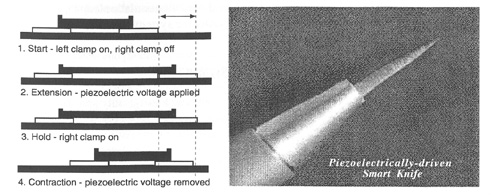
FIGURE 3-4 Microsurgical tool driven by piezoelectric materials. Source: D.L. Polla, University of Minnesota.
diamond films under a program sponsored by the European Community. Considerable work has also been done in the United States at Vanderbilt University and Michigan State University. Polycrystalline diamond films have been grown on silicon from very sparse mixtures of methane (1 percent) in hydrogen (99 percent) at 850°C at growth rates of 0.5 micrometer per hour. Diamond piezoresistors on a diamond diaphragm have been demonstrated as pressure sensors (Wur et al., 1993). Patterning the diamond films is difficult, however, and Wur used a lift-off technique in the cited work. Researchers have also demonstrated ArF excimer-laser ablation, ion etching, and electrolytic etching. Although much work is needed before diamond can be qualified as a mechanical material for MEMS, it may have applications as a low friction coating material.
SURFACE MODIFICATIONS/COATINGS
Processes for surface modification (self-assembled monolayers [SAMs]), deposition, and patterning at submicron levels have been demonstrated for a number of materials. The key process step is the transfer of a catalyst (e.g., a palladium colloid; Xia et al., 1996) from an elastomeric "stamp" to the substrate. This provides the selective pattern for metallization. The overall process has several distinct features:
|
• |
Surface characteristics can be tuned by selecting appropriately functionalized SAMs (e.g., alkyl siloxanes provide hydrophobic surfaces). |
|
• |
These surfaces can be subsequently patterned using a number of wet or dry IC processes (Kumar et al., 1995). |
Many of the deposited films can subsequently be patterned using IC-based equipment and methods. Other surface modification approaches for specific applications, such as biocompatibility, include designing bioactive coatings via protein engineering (Martin, Jiang, and Buchko, 1997).
Plasma-Deposited Polymers
Plasma deposition of polymers results in materials with properties different from more conventionally synthesized polymer films (Yasuda, 1985). By modifying the plasma processing parameters during film deposition, the properties can be tailored. Plasma-deposited films (e.g., parylene) can coat surfaces conformally, even if they have strongly varying three-dimensional topographies (which is an important feature for passivation coatings), mechanical flexibility, or interlayer dielectrics for ICs. For example, a way to plasma-deposit PMMA as a photoresist onto a three-dimensional structure in order to pattern that structure has been demonstrated (Guckel et al., 1988).
Plasma-deposited polymers can also be used as barrier layers, protective layers, or anti-reflection coatings. Pulsed plasmas (PECVD) have been used to coat surfaces conformally with fluorocarbons (TeflonTM -like films; Limb et al., 1996). The methods have been optimized (starting monomeric materials and deposition procedures) to yield film thicknesses of several microns on both planar and nonplanar substrates.
Polyimides
Polyimides are used extensively in IC applications as dielectric layers, masking materials for plasma etching, and alpha-particle protection layers in memory applications. Polyimides have a dielectric constant of about 3.5 and are typically spin-coated and then cured at about 350°C. Preimidized polyimides can be processed at lower temperatures. Polyimides can also be purchased in sheet form under the trade name Kapton™.
Polyimides may be used in the nearer term in MEMS applications as insulating layers, sensing layers (especially for moisture sensors), or flexible membranes. Barth, Bernard, and Angell (1985) and Beebe and Denton (1994) have
reported the use of polyimide as a flexible membrane-support for diode arrays and in biomedical applications. Polyimides have also been used as structural materials for electrostatic actuators.
The major advantage of polyimides is their ease of processing, especially using plasma etching. A disadvantage of polyimides is moisture absorption. Although this is a positive feature for moisture-sensing applications, it can lead to long-term reliability problems, such as increased insulator conductivity, adhesion loss, and corrosion. A number of low-moisture uptake polymers (many of which are fluorinated) have been developed, however, and these can be used in applications where moisture uptake is expected and not desirable.
Conducting Polymers
Early work indicates a potential for using conducting polymers as active sensing or actuation material, based on the changes in elastic moduli, electrical conductivity, and electromagnetic absorption caused by electrochemical doping (Baughmann et al., 1991; Della Santa et al., 1996). Dimensional changes from 0.5 to 10 percent are possible with stimulation voltages an order of magnitude lower than those generally found in electrostatic or piezoelectric actuators, although with comparatively longer cycles times. Della Santa et al. (1996) reported on the use of polypyrole in a conducting-polymer pump diaphragm, but considerable work remains to be done to develop and characterize conducting polymers as useful MEMS materials.
POWER SUPPLIES
As MEMS find broader applications, the demand for autonomous systems will certainly increase. The power source would currently account for the largest part of an autonomous system, however. Thus, reducing the size of power supplies is critical to the design and production of autonomous systems. Research is required on the development of materials with higher energy storage, as well as materials for microscaled fuel cells or miniature combustion devices. In addition, there are opportunities for on-chip and in-module energy converters that can provide electric power from the conversion of electromagnetic radiation, mechanical vibration, or thermal variations.
An alternative approach would be to eliminate power sources and wiring systems entirely and focus on new technologies that could provide power, communication, and control of remote, distributed sensors. For example, power and information could be transmitted into an on-chip radio-frequency (RF) loop antenna, enabling wireless operation of the distributed systems. An alternative to RF is using solar cells and optical-modulation capability to communicate with and power the system remotely via lasers.
SUMMARY
Although using only standard IC materials and processes may produce products with the same levels of manufacturability and reliability as products associated with modern
VLSI devices, new materials and processes will be required for applications requiring enhanced-force microactuation, high-aspect-ratio structures, severe-environment resistance, and enhanced surface properties. In general, future MEMS materials and processes research should be focused on (1) expanding the suite of materials available for IC-like processing and (2) advancing thin-film processing techniques.
Materials that are not usually used in IC processes include magnetic, piezoelectric, ferroelectric, and shape-memory materials. Actuating-force requirements for valve closures and motor drives, for example, are already drawing attention to the advantages such materials would bring to MEMS. Other developments, such as MEMS for optics, biological purposes, chemical-process controls, high-temperature applications, and other hostile environments, will inevitably draw attention to the need for an even broader range of materials.
During IC development, new materials are typically incorporated as thin-films and are produced by a limited number of techniques (e.g., low-pressure CVD or sputtering). Many of these materials either do not show optimal mechanical properties in thin-film form or are difficult to deposit by typical IC-fabrication methods or are incompatible with the microelectronic IC process. For some MEMS designs, it is only possible to apply specialized materials either by incorporating them in a step prior to more conventional processing or by adding them after conventional processing. Either of these options raises the possibility that the technology will be substantially different from better known processing techniques.
Advances in thin-film technologies have enabled the deposition of electroceramic components for the fabrication of sensor and actuators, capacitors, resistors, and magnetic materials on a variety of substrate materials. The deposition techniques discussed in this chapter offer the means to produce thin-films with a variety of tailorable properties and characteristics. Efforts are needed, however, to resolve challenges associated with using these techniques, such as those associated with residual stress, planarization, encapsulation, adhesion, etching selectivity, thin-film cracking, and contamination. Furthermore, adapting the processes discussed above to wafer-based manufacturing presents significant challenges. Finally, as will be discussed in the next chapter, materials for MEMS need to be better characterized; many thin-film materials that are used in the IC industry (e.g., aluminum, silicon dioxide, amorphous silicon, porous silicon, various other deposited and plated metals, and polyimide)
have still not been extensively studied and evaluated for their applicability to MEMS.
Conclusion. The specialized materials and processes discussed in this chapter all require further research to make them compatible with IC-based materials and processes or to permit them to be at the back end or off line in special process areas that will not add prohibitive costs or processing penalties to products. Extending the list of materials for MEMS that can be processed using lithography-based, IC-compatible techniques will be beneficial to MEMS development, provided that a thorough understanding of the properties of these materials is developed. Materials and techniques that might be able to be incorporated into IC-based MEMS in the nearer term include polyimides, magnetic thin-films, HEXSIL, and piezoelectrics.
Recommendation. Research and development should be encouraged to develop new materials that extend the capabilities of MEMS. The new materials should be capable of being integrated, at some level, with conventional IC-based processing.
Recommendation. Research should be encouraged to develop techniques to produce repeatable, high-quality, batch-processed thin-films of specialized materials and to determine the dependence of their properties on film preparation techniques. For some materials, it may be advisable to establish "foundries" that can be used by the entire MEMS community and can serve as repositories for equipment and know-how.
Recommendation. The characterization and testing of MEMS materials should be an area of major emphasis. Studies that address fundamental mechanical properties (e.g., Young's modulus, fatigue strength, residual stress, internal friction) and the engineering physics of long-term reliability, friction, and wear are vitally needed. It is important that these studies take into account process, scaling, temperature, operational environment (i.e., vacuum, gaseous, or liquid), and size dependencies. Studies of the size effects of physical elements, on a scale comparable to the crystallite regions in a polycrystalline material, are required.


