
5
Assembly, Packaging, and Testing
Cost reduction is the most prominent challenge facing the assembly and packaging of MEMS. Packaging currently represents more than 80 percent of the cost of some systems and is often the leading cause of system failure. MEMS packaging is usually approached by individual manufacturers on a specialized, application-specific basis in which problems are solved independently. Very little publicly available work has been conducted on the basic aspects of generic packaging and assembly or on standardized packaging methodologies for MEMS. The imbalance between the ease with which batch-fabricated MEMS can be produced and the difficulty and cost of packaging and testing them limits the speed with which new MEMS can be introduced into the market.
MEMS chip technologies have developed rapidly largely because they share common procedures with conventional microelectronics chip processing. The assembly, packaging, and testing (AP&T) of MEMS, however, often require radical departures from the ''normal" approaches used for electronics. MEMS components may need to interface with light, fluid-pressure, chemical species, and other media without harming the MEMS or the associated electronics. Not surprisingly, meeting these needs requires specialized AP&T approaches, making commonality and cost-effectiveness problematic.
Approaches to MEMS AP&T should make use of the existing semiconductor-industry infrastructure wherever possible. The assembly and packaging equipment infrastructure (beyond those available in the IC industry) should evolve as the volume of commercial applications for MEMS provides market support. Unfortunately, this leaves the pioneers in the field to fend for themselves. They must rely either on their own engineering skills or on attracting the attention of equipment-manufacturing partners. Apparently small departures from conventional electronic-chip practices (e.g., the changes necessary for dicing accelerometer wafers into individual chips) can result in high incremental expenses and costly development delays.
Creating families of generic, standardized, modular AP&T approaches for different classes of MEMS devices could accelerate the overall pace of development. This goal may be inconsistent with low cost, rapid development in the short term, but in the long term it will undoubtedly advance the field. This chapter examines the problems associated with present AP&T methods, considers some of the outstanding needs, and discusses both generic and application-specific approaches.
CONTRASTS BETWEEN ASSEMBLY, PACKAGING, AND TESTING OF INTEGRATED CIRCUITS AND MICROELECTROMECHANICAL SYSTEMS
The electronics industry has expended considerable resources on the development of AP&T techniques for microelectronic circuits, many of which can be applied to MEMS. MEMS typically require extra attention, however, because MEMS often process nonelectronic signals. These signals must be transmitted through the package (when the signal should affect the MEMS), while other parameters must be either transmitted (when the MEMS can tolerate exposure to that parameter) or rejected by the package (when the parameter is not desired or cannot be tolerated). Parameter selection is never perfect, however, and system specifications typically define the allowable cross-talk between desirable and undesirable parameters. A simple diagram of packaging requirements for a MEMS (Figure 5-1) provides a conceptual framework for the packaging requirements and assembly and test methods for MEMS. Determining which parameters are desirable, tolerable, and undesirable, and incorporating this into the design is not a straightforward process, however.
To appreciate the problem, consider a single-domain problem in the electronics industry, "grounding and shielding" for electronic components. Take, as an example, the analog-to-digital converter (A/D), which must maintain a stable, accurate reference voltage on the chip for comparison to incoming signals. The voltage signal is the desired parameter, and all other signals are either tolerated or rejected. Undesirable parameters might, for example, include environmentally caused electrostatic signals or voltages that arise from mechanical stresses that lead to resistance variations via piezoresistive coefficients. Tolerated signals typically include temperature and magnetic field, but the A/D can be made insensitive to both of these by proper design.
MEMS typically include subcomponents that provide transduction between two signal domains. Some examples are:
- an electrostatic comb-drive in which an AC voltage drives a flexure-supported movable part (e.g., Tang, 1990) or a moving capacitor plate that converts mechanical motions into electrical signals (e.g., Analog Devices, Inc.)
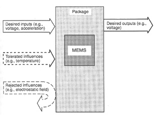
FIGURE 5-1 Block diagram of generic packaging requirements.
|
• |
an impact motor that converts a mechanical resonance into a linear motion (e.g., Lee et al., 1993; Daneman et al., 1995) |
|
• |
a microvalve that converts electrical energy to thermopneumatic force (e.g., Zdeblick, 1996) |
|
• |
a microanemometer that converts fluid flow into an electrical signal (e.g., Tai, 1996) |
|
• |
a flexure beam that converts a mechanical motion to a light modulation (e.g., TI's DMD) |
It is vital that the MEMS be designed to be insensitive to unwanted parameters first and then that the package be designed to admit the desired signal variables (e.g., fluid, thermal, inertial, or optical) with minimal distortion, while screening out unwanted variables. At the same time, reasonable cost, robustness for the intended application, and good manufacturing characteristics, including acceptable AP&T properties, must be achieved. These engineering problems must be solved in order for MEMS to compete successfully with alternative system designs.
INTERFACES
The interfaces between a MEMS component and its operating environment are often troublesome and may present considerable design and manufacturing challenges. Signals admitted to the MEMS package may come from many sources, including electrical, thermal, inertial, fluid, chemical, and optical domains. Output can also vary greatly. Examples include electrical, optical, mechanical, chemical, hydraulic, and magnetic signals (Figure 5-2). Conduits into and out of the packaged MEMS for these signals must be designed to avoid distortion.
The difficulties of designing interfaces vary with the nature of the MEMS. Accelerometer interfacing is relatively easy because it requires only proper orientation and rigid mounting. Interfacing a pressure-sensing MEMS is usually harder because it requires resistance to corrosion from the working fluid and protection against excessive pressures. Chemical-sensor interfacing is inherently difficult, and chemical sensors often fail to provide good long-term stability. Interface considerations can be conceptually segregated into considerations of the chip package, the package environment, and the chip environment. Considerations for interfaces in the biomedical, optical, electric power, fluid, and mechanical domains are discussed below.
Biomedical Interfaces
The long-term impact of MEMS in the biomedical field is likely to be very strong. One application that has already
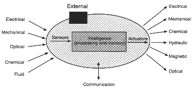
FIGURE 5-2 Schematic diagram summarizing various input/output modalities for MEMS systems. Source: Adapted from a figure by H. Zappe, The IBM Almaden Research Center.
appeared on the horizon is the biochemical laboratory on a chip. Another application is MEMS that would be part of instrumented catheters and endoscopes that could conduct in-body tests and, possibly, therapies. A third application is MEMS elements that might be embedded in living tissue, as pacemakers are. These three applications clearly have different interfaces.
Bringing MEMS technology into the diagnostic/medical market encompasses a number of additional complexities. As mentioned in Chapter 3, a number of efforts are under way to explore new materials and coatings that could increase the applications of MEMS. For regulated medical markets, the packaged test will need approvals that not only demonstrate performance but biocompatibility for specified lifetimes. Furthermore, critical-path testing (e.g., in a hospital environment) requires serviceability within 24 hours.
In the application nearest to commercial reality-the biochemical laboratory on a chip-the silicon surface is partitioned into many small cells, typically smaller than 0.1 mm on one square side. Successive reactions of a small quantity of an analyte with a reagent are initiated in these cells. In at least one version, the outcome is detected by optical means so that a large number of chemical tests can be done in a small, portable unit. Interfaces in MEMS built with these cells must (1) be inert to chemical attack for the useful lifetime of the chip, (2) allow controlled chemical mixing, and (3) allow reliable interrogation of the results. The interfaces are very specialized to the specific uses of the chip. MEMS incorporated into instrumented catheters or endoscopes, as well as MEMS designed for in vivo use, have additional constraints because they will interface with living tissue. There is little doubt that MEMS will play an important role in biomedicine, but it is also clear that considerable work still needs to be done to characterize interfaces for biomedical MEMS.
Optical Interfaces
Current work in the area of optical MEMS is directed toward two goals: building new types of displays based on physical motions of reflecting surfaces; and building new types of fiber-optic systems in which MEMS structures interact with directed light beams. In both cases, the MEMS package must pass light to a surface with which it will interact. Building similar packages has been done for a long time in the IC and photonics industries, which have produced commercial products such as solar cells, LEDs (light-emitting diodes), laser diodes, and light-alterable memory planes (as in the Intel FAMOS chips). Special techniques for surface micromachining MEMS using freestanding silicon nitride films have been demonstrated (Mastrangelo, Muller, and Kumar, 1991), but details of processing, coatings, and coupling to fiber-optic inputs are still in the research stage.
Electrical Power
Insulating, grounding, and shielding electrical components at low-voltage levels are well understood from the electronics industry. Actuators, however, often require drivers that deliver 50 volts or more. The interfaces among the components, the package, and the environment for microdevices operating at these relatively high voltages cannot always be derived directly from typical IC power supplies.
Corrosion problems can threaten the operation of MEMS powering systems because of the different operating environments in which the systems may operate and because not all MEMS devices can be hermetically isolated.
Fluidics
Coupling fluids into and out of MEMS presents significant challenges to systems integrators. Working fluids can range from inert gases (e.g., flow controllers for benign gases) to corrosive or toxic chemicals (e.g., pressure regulators on some gas chromatographs). Often the interface between the fluid and the MEMS requires a compression fitting (e.g., an O-ring seal) or a capillary tube inserted and glued to mate with a micromachined channel. Developing reliable manufacturing methods for interfacing MEMS with fluids requires continued work to support this rapidly growing application area.
The importance of the field of microfluidics is also becoming generally recognized. For example, DARPA has stressed the need for understanding the design rules and fluid dynamics on the MEMS scale from the early stages of their MEMS program funding for visualization tools to the recent Broad Agency
Announcements in the MicroFlumes and related CAD-tools program. Critical elements for chemical and biochemical applications require precise fluid delivery, thermal and environmental isolation, and mixing, as well as materials compatibility for applications and solvent systems. Materials and geometries that can provide specified functions are being addressed at an increasing pace in academic and industrial settings (e.g., monthly conferences on methods and applications sponsored by International Business Communications (IBC) and the Association for Computing Machinery/Special Interest Group on Computer- Human Interactions (ASM/SIGCHI)). Two emerging issues are cost and whether functionality can be integrated on a single device (e.g., lab-on-a-chip) or by coupling high-value elements with generic microconnector elements. These issues are helping drive the exploration of novel materials and methods (see Chapter 3).
Mechanical Interfaces
Thus far, mechanical forces, or torques, are usually transmitted within a MEMS (e.g., in driven gears, as reported by
Sandia Corporation, or in air-driven Pelton wheels made at Bell Laboratories). For applications such as microrobots, movable magnetic read/write heads in a microdisk drive, or MEMS fluidic controls, forces and/or torques must be transmitted as a MEMS output. One approach has been to actuate large arrays of bimorph benders that work in parallel to produce cilia-type motions (Ataka et al., 1993). To make these motions more robust, the Fujita laboratory (where the cilia work was done) has constructed "loop actuators" from sputtered shape-memory-alloy films (Nakamura et al., 1997). More work is being done in this area in Japan than in the United States, but a good deal more research will be needed to produce practical MEMS with output mechanical interfaces.
PACKAGING
The needs for MEMS packaging are as diverse as the applications for which the systems can be used. Some examples include:
- silicon microvalves for gas flow control, some of which are packaged in an almost standard transistor outline (TO8) electrical chip package (e.g., Redwood package
- i-STAT blood-chemistry sensor (Chapter 1), which includes in-package calibration mixtures
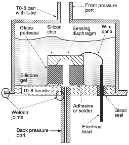
FIGURE 5-3 Silicon pressure sensor. Source: Mallon et al., 1988.
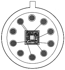
FIGURE 5-4 Accelerometer packaged in IC standard transistor outline (TO) package. Source: Analog Devices, Inc.
-
- pressure-sensing MEMS, for which a multitude of packages are used from many different manufacturers (e.g., Motorola, Honeywell, Kulite, EG&G IC Sensors, NovaSensor, Sensym, Foxboro, and Schlumberger; Figure 5-3)
- accelerometers, which are typically packaged in IC standard transistor outline (TO) and dual in-line (DIP) packages (e.g., Analog Devices, Ford, and Motorola; Figures 5-4, 5-5, 5-6 and Figure 1-5)
Specialized packaging with optically transmissive windows has been developed for TI's DMD chips (Chapter 1).
FIGURE 5-5 Accelerometer packaged in IC standard dual in-line (DIP)

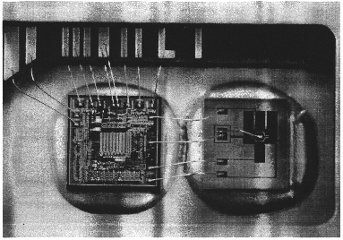
FIGURE 5-6 Two-chip smart accelerometer. The electronic functions are integrated with the sensing function through wire-bond interconnections. Source: Ford Microelectronics.
Ink-jet chips are typically attached to Kapton tape with embedded conductors and contact pads, which can then be glued to the plastic or metal plate in which the ink-jet pen is formed.
The development of packaging is open to creative ideas to enhance performance, and the evolution of packages is often simpler and quicker in practice than making design changes at the MEMS chip level. To date, however, most package development has been for specific products and applications, and very little "generic" packaging methodology has evolved. The development of generic packaging methodologies would eliminate duplication and the reworking of old problems for each new MEMS venture. Although it is not likely that just a few approaches to packaging MEMS will be sufficient, a set of capabilities and methodologies can be defined and developed that address the needs of each basic sensing and actuation domain (e.g., fluid handling, optical coupling, mechanical integration). Generic packaging methodologies would also stimulate the development of packaging equipment that could meet specific MEMS requirements.
Packaging also requires disciplined manufacturing and adequate testing, independent of MEMS manufacturing and testing. Partitioning costs between chip and package will have to be determined on a case-by-case basis. Not much has been published on these issues and associated problems, but there
is a good deal of engineering know-how in the electronics, sensors, and actuators industries. The sections below briefly describe some of the issues involved.
Handling Issues
In many cases, MEMS contain moving parts that are fragile and that may not be protected through the standard IC-wafer passivation step. Because of their vulnerability, extra care must be taken with them. For placement, IC dice can be handled by vacuum pickups that attach to the top surface of the chip. But vacuum pickups may be unacceptable for MEMS dice because of their generally nonplanar surfaces.
Some manufacturers have found ways of using conventional handling equipment for MEMS chips by modifying it to account for specific MEMS sensitivities.
Dicing
For components that are bulk micromachined, the deepetching techniques used as part of the process can sometimes be used to partially or fully separate an individual die from the wafer during the machining process. Another technique that can be used with some devices is bonding an additional wafer or wafers to the first micromachined wafer and then separating the protected sandwiched structures. Many structures that are bulk micromachined cannot be handled in these ways, however, and other techniques must be found for separating dice without damaging or rupturing sensitive structures (e.g., diaphragms) or inadvertently depositing silicon particulates in, around, or under sensitive structures. There are similar problems with parts that are surface micromachined, which has encouraged efforts to encapsulate mechanical parts locally prior to separating the wafer into dice.
Four generic approaches to dicing MEMS wafers have been used. The first approach is to cover the structure with a permanent cap (e.g., Motorola uses this technique for the MAS40 accelerometer). This protects the micromechanical parts so that standard separation techniques can be used, although another piece of silicon-or other material-and additional processing are necessary. There are a number of opportunities for innovations in capping techniques, in the choice of materials for the cover, in the sealing methods, and in the configuration of the protective cover used for interconnection or for active devices or circuits. An interesting innovation is the formation of caps by surface micromachining a mold using HEXSIL (Cohn et al., 1996).
A second approach to MEMS wafer dicing is releasing the mechanical elements after the wafers have been sawed in the standard fashion. Sacrificial release materials and etchants are being investigated that would then allow the release step to be performed after the preliminary packaging steps (e.g., XeF2 post-package release). One drawback of processing dice instead of wafers is that it rules out wafer-level testing because the unreleased MEMS devices are not functional at the wafer-level.
A third MEMS-dicing approach is covering the moving elements with a sacrificial layer that can tolerate sawing or laser scribing and then removing it in a subsequent step. This dicing method also requires processing dice separately and makes wafer testing difficult or impossible. An advantage of this approach is that the sacrificial films are typically polymers, for which dry removal techniques are available (e.g., TI's DMD).
A fourth way to dice MEMS wafers is to protect the released structures with temporary stand-off housings. After sawing and cleaning the wafer using more-or-less standard tooling, the temporary covers are removed. This approach involves extra steps but has the virtue of keeping all steps in a batch-fabrication mode. Analog Devices, Inc., uses this procedure in the fabrication of the ADXL50 air bag-release accelerometer.
Cleanliness
MEMS are extremely sensitive to particulate matter at the back-end stages of manufacturing because of the tiny clearances of the mechanical structures. Special attention to cleanliness during the assembly and packaging steps for MEMS is needed to prevent the introduction of stray particles. Because ICs do not have similar particulate sensitivity, back-end steps can be done in a more relaxed manner. Most existing packaging facilities are not maintained at the level of processing cleanliness necessary for the high-yield packaging of MEMS. Manufacturers must either move MEMS packaging operations into a clean-room space or upgrade the cleanliness of their packaging laboratories.
Stiction
Interfacial adhesion is a major problem for movable MEMS devices (Chapter 2). Because final assembly and packaging processes take place after movable parts have been freed, these processes can have an effect on surface conditions and, hence, on stiction. Using dry-rather than wet-chemical processes in the latter phases reduces the likelihood of stiction.
Packaging Materials
The IC experience in packaging will provide an initial basis for the development of MEMS packaging. Because MEMS have applications in many demanding environments,
however, some specialty materials will probably be necessary. In many cases, experience with hybrid sensing systems will provide guidelines to an enhanced materials-set for MEMS packaging. Adapting these materials to economical and compatible batch processes, however, presents a major challenge. Table 5-1 lists some characteristics of common IC chip packages.
Because of the interactive complexity of the overall IC production process, changes in the IC infrastructure are not easily accepted, and process and materials modifications are made with great reluctance. MEMS production will require a much more flexible mind-set, although intensive research and development will be necessary for any modifications to existing procedures and materials. Frequently used IC materials are user qualified and available at much lower cost than new candidate materials, especially if the new materials are suitable only for customized MEMS applications. Because standard IC-package parts are typically made in batches of one hundred million or more, every effort should be made to use them whenever feasible. A very big payoff will accrue to designers who adapt these package parts to packaging demands for MEMS.
Stresses on Packaging
Differences in thermal-expansion coefficients between packaging materials and the MEMS chips are expected to cause temperature-variable stress patterns in packaged MEMS. These stresses can affect the electrical properties of devices (e.g., through piezoresistance) and can also change the mechanical properties affecting resonator frequencies and residual stresses in delicate parts like membranes. These problems must be alleviated for successful MEMS AP&T.
Fluid Environment
For most ICs, air or dry nitrogen is sealed in a hermetically sealed package. This milieu can be used for a fairly large class of MEMS as well. For some MEMS applications, however, an oil or viscous fluid may have to be incorporated into the package cavity (e.g., the seismic mass in accelerometers may have to be surrounded by fluid to damp shocks or prevent unwanted dynamic responses), or fluids may have to travel through the MEMS (e.g., Redwood Microsystems valves).
Vacuum Packaging
Some MEMS (e.g., resonant sensors) have to be packaged in an evacuated housing. The nature of the materials and sealing processes limits the kinds of packages that can be used, however. A particularly significant challenge for MEMS is developing a vacuum package that seals at lower than 50 m Torr, can be produced at reasonable cost (< $1), and has a life of at least 10 years. Using solder-reflow packaging technology (e.g., from flip-chip processing) to form sealed, controlled-ambient packages at both the die and wafer-level is one possibility. Other potential methods include the formation of a sealed cavity during the fabrication process itself.
However, not all processes or device structures are directly compatible with this method, so new post-processing methods will have to be developed.
ASSEMBLY
If the microelectronic and micromechanical parts of MEMS can be produced using fully compatible processes, the difficult assembly of the two (or more) parts of the system will be avoided in many cases. Most reliability problems in systems can be traced to interfaces, and compatible processing would prevent the introduction of reliability problems during assembly. Therefore, an important goal to enhance the development of MEMS is to enlarge the design space available to MEMS that can be compatibly batch processed. Despite the advantage of fully integrating micromechanical and microelectronic parts in a single batch process, significant limitations would also be introduced (e.g., requiring the use
TABLE 5-1 Characteristics of Common IC Chip-Level Packages
|
Hermetic Package Types |
Seal Material |
Maximum Process Temperature |
Issues |
Figure |
|
Welded package (can) |
metal-to-glass |
< 150°C |
Material costs, accurate lead placement, diminishing user base |
5-4 |
|
Side-brazed ceramic |
solder |
< 230°C |
Requires gold, expensive (> $1/package) |
5-5 |
|
Cerdip |
glass |
430°C |
High seal temperature |
1-5 |
of a silicon substrate would result in stringent processing and design revisions). But special needs and difficult processing challenges will almost certainly mean that mechanical and electrical processing for many future products will have to be separated. For this reason, techniques for electromechanical MEMS assembly are an important factor to consider.
A different class of assembly problems is introduced if micromechanical parts have to be assembled to form micromechanisms. Because of their tiny size, the mechanical assembly of micromechanisms is extremely difficult and is avoided as much as possible. In some technologies and for some devices, however, mechanical assembly may be unavoidable, and microassembly tools, some of them built using MEMS procedures, will have to be used.
Procedures that have been used to assemble micromechanical and microelectronic parts into MEMS thus far range from traditional hybrid-packaging methods to mating IC-fabricated electronics with micromechanical devices fabricated by a micromolding technique, such as LIGA. Most of the MEMS assembly available at this time is being used to integrate microsensing devices with electronics. Although three basic methods of electronic-MEMS integration are available (monolithic, flip-chip, and hybrid), only flip-chip and hybrid require the physical assembly of separate components.
Hybrid Assembly
Hybrid assembly is the most common method used today for assembling MEMS. Hybrid assembly methods range from simple systems, such as the Ford Microelectronics accelerometer (Figure 5-6), to the complex, multichip, multilevel assembly used in the dissolved-wafer process by a group at the University of Michigan (Figure 5-7). Hybrid assembly usually involves bonding two or more die to a single package, carrier, or substrate board, and then the interconnection of the separate chips by wire-bonding and/or package wiring. Hybrid assembly for MEMS can be done using equipment, materials, and testing methods common in the IC industry, including tools for die attachment, chip pinout, and heat removal, as well as for the measurement of signal-rise time, power-lead inductance, power-supply current, and interline coupling. The design of hybrid assembly also must consider factors like the wiring configuration for multiple chips and propagation delays as the signal is relayed between chips (NRC, 1990).
Using a flip-chip attachment (e.g., solder-bump technology) is a well established practice in the IC field, but the materials, processing, reliability, and manufacturing features required to make it viable for integrating separately fabricated micromechanical and microelectronic MEMS parts have only begun to be investigated (Markus, Koester, and Dhuler, 1994; Figure 5-8). Many issues need consideration and evaluation, such as the metallurgy of the solder attachment pads; the mechanical rigidity of the attached pair; the use of solder flux that requires liquid cleaning; the effect of the package flex on micromechanical properties and long-term stability of MEMS; the use of backfill material between the attached chip and the substrate; the presence of access holes to the "hidden" chip face; and the probability of survival in the environmental requirements.
Assembly of Micromechanical Parts
A special class of problems arises in cases where the subassembly of micromechanical parts is necessary to form mechanical elements. If at all possible, batch fabrication of in situ-assembled parts (as in surface micromachined rotating micromotors) is preferable because of the scale of most micromechanisms in MEMS. If in-situ fabrication is not
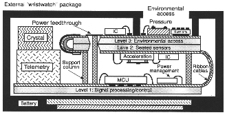
FIGURE 5-7 Detail of a multiplatform hybrid package showing feed-through, interconnect, and support features for an environmental monitoring cluster system. Source: Wise, 1995.
FIGURE 5-8 Flip-chip attachment of two die to form an integrated system. One die is an IC, the other a MEMS chip. Source: MCNC MEMS Technology Applications Center.
possible, methods of assembly will have to be devised. Ideas for microassembly operations can be obtained from present manufacturing experience in other industries that must gather and assemble very small pieces using specialized machinery (e.g., producers of computer disk drives). The scale of the MEMS devices will typically place new demands on assembly techniques, however, and research on ways to meet these demands will be necessary.
One inventive approach that can address a limited class of microassembly problems has been to make microparts with characteristic insertive geometries that fit in complementarily formed receptive geometric shapes (e.g., Yeh and Smith, 1994). Random mixing of the two systems results in assembly of the microparts similar to the joining-together of microbiological systems. This process has been used extensively throughout the milliscale assembly domain. A critical issue for this "batch assembly" approach is the effect of the liquid milieu in which the parts are randomized (usually by vibrating it), which can have devastating effects on yield for parts susceptible to stiction. If the microparts have to be manipulated one at a time, systems that can pick up, place, and assemble them must be developed. This approach to the microassembly problem is being addressed by a few research projects that use MEMS technologies to build microtweezers, micromanipulators, and pickups. (e.g., Oak Ridge National Laboratory, The Berkeley Sensor & Actuator Center). Given enough impetus, fully automated systems for subassembling micromechanisms will probably be developed. Some of the outstanding issues that need to be investigated are listed below:
|
• |
methods for array or row pick-and-place and for reorienting microparts via rotations about one or several axes |
|
• |
maintaining tolerances in mating microparts |
|
• |
controlling delicacy in interfacing the microtweezers and the potentially fragile micropart |
|
• |
operating at speeds sufficient to qualify the microassembly process for reasonable use in a commercial process |
|
• |
the degree to which procedures can be used with alignment pins, threaded assemblies, and other macroscopic design techniques |
|
• |
maintaining sufficient precision of micropart production to permit the use of subassemblies-precision in MEMS-level micromechanical parts is typically significantly poorer than in macroscopic parts |
Parts with large assembly tolerance can be assembled using robotic systems that can join a fluid port to a capillary with compression fittings or that can align a glass cap over a chip already bonded to a ceramic substrate. Technologies like LIGA are the impetus for the assembly of parts with very tight geometric tolerances. Recently, alignment-pin assembly fixtures have been used to assemble fluid microflow structures (Figure 3-3), stacked vertical magnetic actuators, and a series of magnetic linear actuators (Figure 5-9). For the microflow device, pin alignment holes were fabricated in the corners of the two mating pieces, and glass capillary pins were used to align and secure the two 500 µm thick pieces for subsequent thermal bonding. This form of pin-assembly has only been done manually, however.
Another assembly method for MEMS is physical bonding (fusion or anodic) of two or more wafers to assemble microparts into a micromechanical device (Roylance and Angell, 1979; Ko, Suminto, and Yeh, 1985; Peterson et al., 1988). Figure 5-10 shows the formation of a thermopneumatic microvalve using glass-to-silicon anodic wafer bonds. The silicon wafers are patterned and etched separately and then precisely aligned using equipment similar to equipment used in IC processing for lithography. The silicon wafers are then anodically bonded. This is basically a "sheet" method of assembly because an entire wafer surface of devices numbering into the thousands can be simultaneously assembled. The large-scale production of pressure sensors by Ford Motor Company is based on this technology. A related technique using other materials is employed by Hewlett-Packard to assemble their ink-jet print-heads by positioning a thin nickel sheet over the closely spaced drivers formed on a silicon wafer.
Extending these wafer-bonding batch assembly methods to other microstructures will require additional work. Some of the challenges facing large-scale sheet assembly are the accuracy of placing parts both within a sheet and from sheet to sheet. Additional factors that complicate this method are
FIGURE 5-9 Assembled magnetic linear actuator. The coils are inserted into "spring fittings" and the shuttle/suspension assembly is inserted onto mounting pins located at the suspension anchor points. Source: Guckel et al., 1996b.
right-to-left or top-to-bottom shifts that occur when sheets, wafers, or assembly jigs translate through mirror, radial, or linear translations prior to assembly (e.g., face-to-face assembly aligns the right side of one sheet to the left side of the other). Once sheet-to-sheet (or wafer-to-wafer) assembly is completed, the separation of the individual die from the sheet can lead to additional complications, especially if the bonding pads formed on one wafer have been overlapped by the attached wafer. For biological applications, lower temperature bonding methods will have to be developed.
The assembly of optical fibers with other components has been done for some time using basic micromachining techniques. By inserting a fiber into a v-groove etched in a silicon wafer, the fiber can be aligned with other elements fabricated either in the wafer or on the wafer surface (Solgaard et al., 1995). With this method, however, the alignment between the fiber and other components can have errors of tens of microns, requiring further micromanipulation of either the fiber or the optical components. Work on addressing this issue through the use of movable microalignment structures (e.g., active alignment structures, moving mirrors, lenses, and fiber grips) is under way (Solgaard et al., 1995).
STANDARDS, TESTING, AND RELIABILITY
Functional and reliability testing are basic requirements for all manufacturing. Testing MEMS presents considerable challenges and typically requires not only electrical measurements but also environmental stimuli, such as fluid, shock, vibration, and temperature. Testing and characterization methods and structures suitable for the materials and domains of MEMS have yet to be developed. Standards organizations (e.g., American Society for Testing and Materials [ASTM] and National Institute of Standards and Technology [NIST]) and professional technical societies (e.g., Institute of Electrical and Electronics Engineers [IEEE]; American Institute of Mining, Metallurgical, and Petroleum Engineers [AIME]; and American Society of Mechanical Engineers [ASME]) will be invaluable for establishing standards, but significant interaction with the MEMS community needs to be instigated.
Manufacturers have traditionally qualified products using accelerated-aging tests carried out in extreme environments. The conditions of these tests need to be determined, and the standards for passing them must be established. A significant amount of effort has been expended to define and validate accelerated test methods for ICs and mechanical materials separately, but only some of this background work is directly applicable to MEMS. A challenge for MEMS is to evaluate the specifications that already exist and to incorporate or elaborate on them where appropriate. A suitable place to begin might be with military applications, where program unique military specifications to ensure that systems or components will perform as expected (MIL-STD-490A) have already been established. The suitability of these specifications to MEMS in a limited, fairly well developed category (e.g., accelerometers) could be tested with the goal of evolving product-level testing to qualify MEMS for military use.
In the IC field, a great deal of important data about reliability has been contributed by academic researchers. Although academic research has not been focused on reliability in the MEMS area, this should be encouraged. Figure 5-11 shows typical processing specifications in the IC world, from die level testing to component/system-level testing. Better methods for testing and qualifying MEMS at all levels of the figure must be developed.
FAILURE ANALYSIS
Understanding and predicting failures is critical to the development of reliable products. Predicting failures is also essential for the establishment of specifications and standards. Understanding system-failure modes and processes requires failure analyses of systems. First, the definition of failure for a component or system must be established. A reasonable definition might be worded: "A failure occurs when there is a change in the performance of a component or
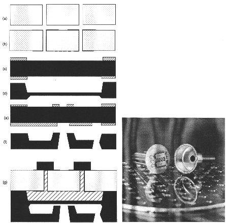
FIGURE 5-10 Packaged, normally-open microvalve (a 100 mm diameter silicon wafer provides a size reference) and process flow for fabrication of a normally-open, thermopneumatically-actuated microvalve: (a) holes are ultrasonically drilled in Pyrex wafer; (b) Pyrex wafer is metallized; (c) membrane wafer is defined lithographically (using gold, oxide, and photoresist masks); (d) membrane wafer is etched in KOH and masking materials are stripped; (e) orifice wafer is defined lithographically (using gold, oxide, and photoresist masks); (f) orifice wafer is etched in KOH and masking materials are stripped; (g) in the final steps, membrane and orifice wafers are fusion bonded, Pyrex is bonded to this sandwich anodically, and the thermopneumatic cavity is filled with liquid and sealed with silicon caps. Source: A. Henning, Redwood Microsystems.
system resulting in the inability to use the component or system as designed or intended.'' The goals of failure analysis are threefold: to identify the cause of the failure; to identify the critical features or parameters of the component or system; and to redesign the component or system based on the critical parameters to reduce the chances of failure. Failures in MEMS are caused by mechanical failure; electrical failure; electromechanical failure (e.g., failure of an actuated mechanical part); or interface failure (e.g., failure at a seal).
Progress in MEMS will be significantly aided by collecting failure-analysis information in an accessible database. Industry does not generally share failure-analysis information for competitive reasons. In the IC world, however, there is a substantial open data bank of failure analyses because of the existence of foundries for many of the leading processes. MEMS is currently not yet defined by a common, standardized set of processes for commercial operation. The few standardized processes that do exist, at MCNC and Analog Devices through its multiproject runs, are contributing to a public data bank on failure modes in MEMS processing.
The data bank for MEMS should include: pertinent information on the component, system, and tests performed; basis
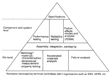
FIGURE 5-11 Specifications at all levels of testing. Source: Howard Last, Naval Surface Warfare Center.
of design for the component and system; "traditional" analysis tools (e.g., optical microscopy, circuit probing, and scanning electron microscopy) for identifying causes of failure; and appropriate methods for studying failure utilizing MEMS component or system-specific features (e.g., self-test capability). The following information is needed to perform a failure analysis: system identification (e.g., process lot); documentation of the fabrication process; documentation of performance- and life-testing for the same process lot (e.g., test conditions, numbers of cycles prior to failure, records of output signal and load as a function of time or number of cycles); and documentation of actual system testing and operational history.
SUMMARY
Although packaging, interfacing, and assembly have attracted less interest than the more glamorous areas of device and process development, these are critical final production steps and can easily represent up to 80 percent of the cost of a component. Along with testing, packaging, interfacing, and assembly represent critical stumbling blocks to the development and manufacture of commercial and military MEMS. Efforts to expand the currently small knowledge base in this field and to disseminate the results aggressively could have a significant positive effect. One of the most urgent needs is for generic packaging methods that would eliminate the need to invent or develop a new package for each new MEMS product. Obviously, there will never be a universal package because of the many application areas of MEMS, but it is possible to define a class of materials, procedures, and package designs that are suitable for the basic needs of MEMS in many areas (e.g., fluid handling, optical coupling, physical sensing). Generic packaging methodologies would also facilitate the evolution of packaging and testing equipment that can address specific MEMS requirements. Improvements in MEMS packaging and assembly will require better understanding of the interfaces between MEMS components and their operating environments, as well as better test methods and standards.
At the small scales at which MEMS are configured, material behavior is more influenced by surface-driven effects than by volume or bulk effects. If the interfaces act as electrical contacts (e.g., in MEMS microrelays), additional wear, corrosion, frictional effects, and contact forces are present. Surface-to-surface sticking (stiction) can also be important in surface-driven processes. The interfaces between a MEMS and its operating environment can also be troublesome and can demand considerable design and manufacturing effort. Signals admitted to the MEMS package can have electrical, thermal, inertial, fluid, chemical, optical, and possibly other origins. Outputs may include electrical, optical, mechanical, chemical, hydraulic, or magnetic signals, singly or in concert.
Standard test devices and methods are required to determine the mechanical properties of MEMS devices, to demonstrate the repeatability and reliability of mechanical devices, and to facilitate quality-control practices. Package-level testing
is currently the most common way to measure MEMS performance, but the development of in-process wafer-level testing will be necessary for low-cost manufacturing. Wafer-level testing of MEMS presents special challenges that are often product dependent. Nevertheless, generic test-structures that indicate basic mechanical properties of MEMS materials at the wafer-level should be developed and characterized. As more and more industries, universities, and other research groups enter the MEMS field, it is also becoming increasingly important to provide accepted standards that can be used for comparison.
Conclusion. Packaging, which has traditionally attracted little interest compared to device and process development, represents a critical stumbling block to the development and manufacture of commercial and military MEMS. The imbalance between the ease with which batch-fabricated MEMS can be produced and the difficulty and cost of packaging them limits the speed with which new MEMS can be introduced into the market. Alleviating the difficulties of packaging will require a better understanding of (1) the effects of internal friction, Coulomb friction, and wear at solid-solid interfaces and (2) the influence of interfaces on performance and reliability. Test and characterization methods and metrologies are general requirements for continued MEMS development and manufacturing advances. Finally, expanding the small knowledge base in this field and disseminating advances aggressively could have a profound influence on the rapid growth of MEMS.
Recommendation. Research and development should be pursued on (1) MEMS interfaces with operating environments, (2) MEMS packaging, and (3) MEMS assembly into useful engineering systems. The goal should be to define, insofar as possible, generic, modular approaches and methodologies and to extend batch-processing techniques into the various back-end steps of production.
Recommendation. Surface and interface studies should be pursued to address questions associated with contact forces, stiction, friction, corrosion, wear, lubrication, electrical effects, and microstructural interactions at solid, liquid, and gaseous interfaces. Engineering design and manufacturing solutions to these problems should also be pursued.
Recommendation. Standard test methods, characterization methods, and test devices that are suitable over the full range of materials and processes for MEMS should be developed and disseminated. Ideally, metrology structures will be physically small, simply designed, easily replicated, and conveniently and definitively interrogated. MEMS engineering standards should be similar to those already established for materials and devices in conventional sizes by organizations such as NIST, ASTM, and IEEE.


