
1
Background
As we approach the twenty-first century, the continuous ability of engineers to shrink electronic devices while simultaneously increasing their performance has profoundly affected both technology and society. A half-century ago, the transistor ushered in the solid-state era of electronics and began a procession of events that drove most earlier technologies (based on vacuum tubes) from the field. In a series of major strides, silicon became the material of choice, planar processing was introduced to make photolithography possible, and the integrated circuit (IC) was born. The planar-processed IC is, without question, a great engineering achievement, making possible the low-cost production of a myriad of electrical systems, including the memory chip and the microprocessor. Silicon very large scale integrated (VLSI) chip technology seems destined to continue the trend toward smaller sizes, higher performance, and greater functionality for at least another 20 years.
The success of solid-state microelectronics ignited the spark of a similar revolution in microscopic systems in the nonelectronic world and resulted in the adaptation of the VLSI tool-set to the manufacture of systems that interface with the nonelectrical environment. Research in this field began in the 1950s with breakthrough studies on piezoresistance in silicon. Single-crystal silicon's piezoresistance and elastic behavior made it an excellent material for the production of sensing devices and led in the 1960s to the development of the first silicon pressure sensors. In the 1970s, the field grew as pressure-sensor production increased and the first silicon accelerometers were developed. The field was dubbed MEMS (microelectromechanical systems) in the late 1980s after silicon fluid valves, electrical switches, and mechanical resonators were developed and marketed (see Box 1-1).
MEMS contain mechanical elements that are built on such a small scale that they can be appreciated only with a microscope. MEMS elements interface with nonelectronic signals and often merge signal processing with sensing and/or actuation. MEMS may contain mechanical parts, such as pressure sensors, flow sensors, or optical-beam handling devices. Some fully integrated MEMS are designed using computer-aided design (CAD) techniques based on VLSI and mechanical CAD systems; they are batch-fabricated using VLSI-based fabrication tools. Like VLSI, MEMS are becoming progressively smaller, faster, and more functional.
The U.S. Department of Defense and the National Aeronautics and Space Administration requested that the National Research Council conduct a study (1) to review current and projected MEMS needs based on projected applications, (2) to identify shortcomings in present and developing MEMS technologies, (3) to recommend how MEMS can best use advanced materials and fabrication processes to overcome these shortcomings, and (4) to recommend research and development (R&D) areas that would lead to the necessary advances in materials and fabrication processes for MEMS. The Committee on Advanced Materials and Fabrication Methods for Microelectromechanical Systems was convened, under the auspices of the National Materials Advisory Board, to conduct this study and write this report.
The MEMS track record already includes several commercial successes (e.g., pressure sensors, accelerometers, and ink-jet print-heads) that provide a compelling case for further development. Like any other developing field, MEMS' commercial successes coexist with less mature products that have yet to establish a customer base (e.g., optical-mirror arrays for display purposes, microphotonic switching devices, actuated
|
BOX 1-1 In the early 1980s, a general consensus was reached about creating microsystems, and many names for the emerging field were coined. Not surprisingly, they met with varying degrees of acceptance, and, also not surprisingly, the names were not consistent internationally (even if all of them were in English). Several names began to dominate:
The two most resilient names are microsystem technologies and microelectromechanical systems with their respective acronyms, MST and MEMS. The preferred label in the United States is MEMS, whereas MST is used in Europe and, to a lesser extent, in Japan To some observes, these choices reflect a stronger emphasis on technologies in Europe and Japan and a stronger focus on systems in the United States. |
gas-flow microvalve systems, and microbiological systems). There have also been several programs aimed at the commercial development of MEMS that have been discontinued, including those supporting automotive fuel-injection manifold air-pressure-sensing MEMS, because they were not found to be cost effective. In other applications, such as microvalving and suspension control, the adoption of MEMS has been slow. Displays based on MEMS, such as the mirror array by Texas Instruments (described below), also face intense competition from newly developed liquid-crystal designs. Although many observers regard these developments as normal growing pains for a new technology, others have serious reservations about the future of the field.
The remainder of this chapter presents an overview of current trends in the MEMS market. The chapter is divided into three sections. The first section describes MEMS that are already successful on the market, such as thermal ink-jet print-heads and accelerometers. The second section reviews MEMS technologies currently under development that show significant commercial potential, such as chemical-sensor arrays and display technologies based on mechanical reflecting elements. The third section discusses some future possibilities and long-range research opportunities.
COMMERCIAL SUCCESSES
Although most people still consider MEMS a technology of the future, a considerable number of people already use MEMS-based devices every day. The ink-jet cartridges in many commercial printers and many of the accelerometers used to deploy air bags in cars are MEMS devices. This section examines the commercial success of ink-jets and accelerometers.
Thermal Ink-Jet Printing
The thermal ink-jet print-head is the largest commercial success story for MEMS technology in terms of both unit sales and dollar amounts. Thermal ink-jet cartridges currently dominate the ink-jet printing market and account for well over a billion dollars per year, independent of the printers in which they are used. Ink-jet printers (both thermal and piezoelectric) typically cost less initially than dry-toner laser printers and, despite their slower speed and higher per-page cost, are often the solution of choice for low-volume print runs. Vendors of ink-jet printers include Canon, Epson, Hewlett-Packard (HP), Lexmark (formerly a part of IBM), and Xerox.
The concept of drop-on-demand thermal ink-jet printing was developed independently, and nearly simultaneously, by HP and Canon. HP commercialized the "Thinkjet" in 1984 using a glass substrate, while Canon commercialized its version as the "Bubblejet." Later print-heads used silicon

FIGURE 1-1 Cross-section of an integrated thermal ink-jet chip. This instantaneous view shows an ink droplet being ejected from the firing chamber by the "drive bubble" created by resistive heating. An NMOS (N-channel metal oxide semiconductor) transistor is associated with each firing chamber. Transistor addressing is achieved by a row-column address scheme. Source: Adapted from Beatty, 1996.
substrates to take advantage of the widely available equipment set and fabrication methods for silicon.
Thermal ink-jet print-heads (or pens) are packaged as replaceable drop-in cartridges on the order of 9 to 50 cm in volume. They usually comprise a supply of ink and an array of microscopic heating resistors on a silicon substrate mated to a matching array of ink-ejection orifices (Barth, 1995). In some designs, the associated active electronics are on the same substrate. These pens constitute the enabling technology-base for printers ranging from battery-powered, portable units to large-format bed plotters. Figure 1-1 shows a cross-section of a thermal ink-jet head with integrated active electronics. The orifice plate of the print-head is made of plated nickel laminated on top of a polymer barrier layer. Although producing this arrangement requires a departure from purely lithographic batch processing, the lamination process has been demonstrated to be cost effective for the large volumes demanded by the ink-jet market.
Figure 1-2 illustrates the decrease in ink-drop weight over time for one family of ink-jet printers. Image quality is greatly
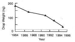
FIGURE 1-2 Evolution of ink-jet drop weight versus time. Drop weights below the dotted line can produce photographic-quality images. Source: Beatty, 1996.
influenced by ink-drop weight. The horizontal dotted line in the figure represents the minimum drop-size the human eye can perceive. Drop weights below this threshold can produce photographic-quality images. Ink-jet printing thus has the potential to replace silver halide film as a medium for photographic prints. This prospect is expected to cause some dislocations in the photographic industry as electronic cameras that can be easily interfaced with computers and printers begin to produce high-quality graphics for presentations and other uses. Ink-jet technology is also being studied for possible use in the deposition and patterning of sensitive biochemicals (e.g., clinical-assay reagents) in the production of biomedical devices.
Ink-jet technology has evolved, for the most part, via internal investment by commercial companies. These investments have already reaped significant benefits in the marketplace. Approximately 67 million ink-jet printers were in existence worldwide as of 1995 (Barth, 1995). This large base of printers promises a dependable revenue stream for vendors of disposable ink-jet pens. Customers can expect continued improvement in print quality and speed at a reasonable cost.
Accelerometers
Government mandates for passive-restraint devices in automobiles created a large market for air bags (i.e., passive restraint devices in which an explosive gas-generating charge is triggered by an electrical signal from a crash sensor). MEMS technology has been adapted to this market because it promises high reliability, ruggedness, and cost effectiveness. Several MEMS technologies have vied for the crash sensor market, which requires both self-testing (for reliability) and accurate, rapid, acceleration sensing (for decision making). Developers in the United States include Analog Devices, Inc., Delco Electronics, Ford Motor Company, General Motors, EG&G IC Sensors, NovaSensor, and Motorola. A large producer in Europe is SensoNor of Norway.
The largest market penetration thus far for board-mountable integrated accelerometers has been achieved by Analog Devices and SensoNor. These companies took very different approaches to the design of crash sensors. Analog Devices used single-chip bipolar-complementary metal-oxide-semiconductor (Bi-CMOS) processing (e.g., the ADXL50); SensoNor employed a two-chip approach (e.g., the SA30).
The Analog accelerometer is based on techniques that were originally developed at the University of California at Berkeley in the early 1980s. These techniques reached their present level of sophistication via continued R&D investment by academia, industry, and government. The accelerometer chip employs a suspended polycrystalline-silicon seismic mass tethered by four polysilicon beams to the substrate at their distal ends (Figure 1-3). Fingers extend laterally from the movable seismic mass perpendicular to the sensitive axis.
Other fingers fixed to the substrate reach between the
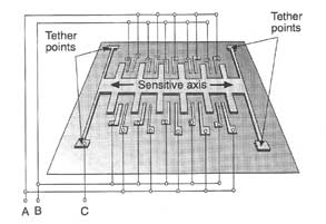
FIGURE 1-3 Schematic illustration of the sensing element of the ADXL50 accelerometer. Source: Analog Devices, Inc.
movable set and apply coulombic force when voltages are applied between terminals A, B, and C. The voltage required to hold the seismic mass motionless relative to the static fingers provides the acceleration signal. This "force-balanced system" uses a precision measurement method that is well established but typically available only in very expensive systems. The sensing element is the heart of an accelerometer chip (Figure 1-4) but occupies less than 1 mm2 on a chip that is 9 mm in area. The sensing element can be combined with a Bi-CMOS electronics fabrication process with only moderate increases in complexity, which means the combined sensor and circuit on one silicon chip can be produced at low cost.
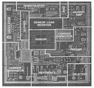
FIGURE 1-4 Annotated photomicrograph of an ADXL50 single-chip accelerometer. The sensing element in the center is surrounded by active electronics. The motion-sensitive direction lies in the plane of the chip and is the vertical axis in this photograph. Chip size is 3 mm x 3 mm. Source: Analog Devices, Inc.
The SensoNor accelerometer sensing element is a single crystal resonant beam that bridges a cavity in a silicon chip. Stress on the beam from acceleration perpendicular to the plane of the chip causes a change in the resonant frequency. This frequency change is detected by electronics contained on a separate chip, and a signal is emitted to deploy the air bag. The sensing and electronics chips are packaged together in a single surface-mounted package. Several other concepts for accelerometers (e.g., Ford Motor Company's silicon-on-glass torsional accelerometer [Spangler and Kemp, 1995] and Motorola's family of silicon capacitive micromachined accelerometers [Ristic et al., 1993]) also rely on dual-chip approaches (e.g., Figure 1-5).
These two device types have not yet reached the automotive market in large quantities. Like SensoNor, these companies have decided that their cost and performance goals can be met at this time by combining a simple sensing chip with a separate electronics chip. It appears that several approaches to crash sensing are suitable from a performance perspective so that cost considerations alone are likely to dictate which ones dominate the market in the long run.
NEWLY INTRODUCED PRODUCTS
High-resolution displays and chemical-sensor arrays are two examples of emerging MEMS products with the potential for strong market growth.
High-Resolution Displays
Displays have long been dominated by cathode-ray tubes (CRTs) and liquid-crystal display (LCD) monitors. CRTs are
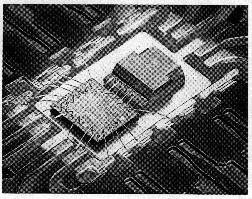
FIGURE 1-5 Motorola accelerometer chip (upper right) and electronics chip (lower left) packaged together on a metal lead frame. The sensitive direction is perpendicular to the upper surface of the accelerometer chip. Source: Motorola.
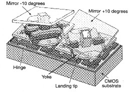
FIGURE 1-6 Two pixels in the Texas Instruments mirror array. Mirrors are shown as transparent. Source: Hornbeck, 1997.
typically too large and too bulky for portability and are limited in screen size by several factors including the need to support an internal vacuum against atmospheric pressure. Although LCDs have traditionally been limited in brightness, contrast, speed, and resolution, they have improved greatly with recent LED (light-emitting-diode)-LCD projection displays. As a result, the LCD market has been expanding.
Mirror array technology is a revolutionary new technique made possible by MEMS. Mirror arrays show promise for the production of large, lightweight, high-brightness, high-contrast, and high-resolution displays at reasonable cost. Texas Instruments (TI), aided by U.S. government R&D funds, has dedicated more than a decade to the development of array micromirror technology for video, computer, and presentation displays. TI calls its approach digital light processing (DLP) and its basic device a digital micromirror display (DMD). The DMD consists of many tiltable mirrors and associated circuitry that are batch-fabricated on a single silicon chip. The mirrors are individually addressed and tilted by coulombic force either toward or away from a collimating lens that collects the light to be projected on the display screen. Each mirror is electrostatically deflected by electrodes beneath it (Figure 1-6). The mirrors, which are less than 20 m on an edge, are closely spaced to give a maximum "fill factor" and make as much of the chip area a reflecting surface as possible (Figure 1-7). Gray scale is provided by varying the percentage of time each mirror directs light to the display screen. Either one color wheel or three separate chips provide multilevel color capability. The first DMD micromirror (and hence pixel) arrays have 800 x 600 pixels per chip.1 Chips with 1024 x 768 pixels are currently under development (Hornbeck, 1996).
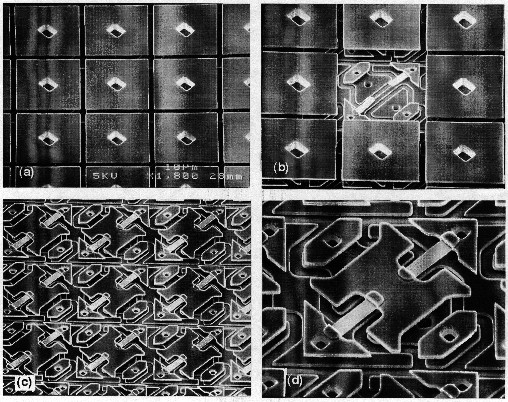
FIGURE 1-7 Scanning electron photomicrographs: (a) completed digital mirror display (DMD) chip; (b) completed DMD chip with mirror layer and yoke-and-hinge layer removed for one pixel; (c) completed DMD chip with mirror layer removed; (d) close-up of one pixel with mirror layer removed. Source: Hornbeck, 1995.
Alternative MEMS display technologies are under industrial development elsewhere (e.g., Silicon Light Machines in the United States and Daewoo in Korea), but dates for their commercial introduction are still uncertain.
Chemical-Sensing Arrays
The high cost associated with diagnostic testing is endemic to the cost of health care. MEMS technology can provide rapid, disposable, inexpensive, and reliable testing that requires small sample sizes and is suitable for use at bedsides or in doctors' offices. A growing number of companies have significant programs under way to produce MEMS for chemical sensing that will reduce the cost and improve the quality of testing (e.g., Affymetrix, Perkin-Elmer Applied Biosystems, and Caliper). The objective of these programs is to develop systems that offer one or more of the following improvements: higher throughput, lower cost per test (either by minimizing materials requirements or complexity), or field portability.
The first chemical sensor-chips have only recently come onto the market in a portable format configuration and have yet to return sizable profits to manufacturers. For example, the i-STAT portable clinical analyzer (PCA) is a hand-held unit that can analyze 60 µL of whole blood using disposable cartridges. The PCA employs micromachined electrochemical sensors (biosensors) to measure sodium, potassium, and chloride ions, as well as urea, glucose, and hematocrit concentrations. The heart of the i-STAT system is a disposable cartridge, which includes a molded frame with an entry for samples and calibration reagents that are distributed to the sensors located in the hand-held reader. The system measures 20 x 6.5 x 5 cm, weighs 539 g, and is powered by two 9V batteries.
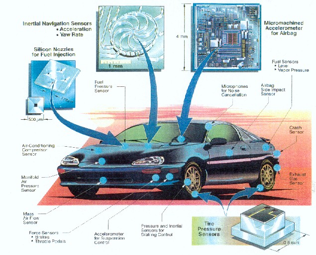
FIGURE 1-8 Concepts for applications of automotive sensors and accelerometers. MEMS could be used to activate suspension systems, control engines and emmissions, control vibration, and cancel noise. Source: D. Thomas, Perkin-Elmer Applied Biosystems, based on concepts by G. Kovacs, K Petersen, and M. Albin.
Packaging takes on special importance for chemical-sensing applications, as does the need for fundamental studies of flow in small channels and of liquid-solid interface effects. These areas still present challenges, but the barriers are surmountable. Indeed, much work is under way to bring the promise of MEMS to fruition in this area.
LONGER-RANGE OPPORTUNITIES
In some instances, MEMS have made the transition from research to commercial products, some with very large markets. Until now, however, MEMS have remained mostly in the first phase of product realization, which offers an improvement over what is already on the market. For example, the MEMS accelerometer does not enable the implementation of air-bag safety systems; rather MEMS accelerometers offer cheaper systems and better performance. MEMS technology is now poised to enter a second phase of product realization, which is marked by the creation of entirely new markets. As a fully integrated system, a MEMS can provide products that know where they are, what is occurring around them, and how to affect a particular outcome.
Future MEMS applications will not only allow information gathering and communication at a distance, but they will also sense and control environments remotely at low cost. With this combination of capabilities, MEMS will play a key role in large sectors of the economy, including health care, transportation, defense, space, construction, manufacturing, architecture, and communication systems. A few potential examples of the opportunities for MEMS are described below.
Transportation
MEMS can improve the performance and reliability of all vehicles, especially automobiles and airplanes. Sensors and accelerometers could potentially be used in the automotive industry, for example, for active suspension systems, engine and emissions control, vibration control, and noise cancellation (see Figure 1-8). In the aerospace industry, MEMS sensors could be used for detecting flow-instability, avoiding stalls, and monitoring structural integrity, as well as for controlling engines and emissions and canceling vibration and noise.
Biomedical and Health Care
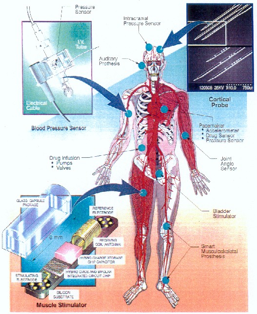
In addition to using MEMS to reduce the high costs associated with diagnostic testing, researchers are investigating using MEMS to sense the condition of the body and actuate implanted reservoirs to release controlled doses of medicines (Figure 1-9). Portable MEMS-based analytical instruments are under development that will enable communication and control with remote locations and permit the exchange of information with remotely located experts.
Information Technology
With microactuated read-write heads and instrumented microminiature head housings, researchers predict a tenfold increase in recorded information density in MEMS-engineered microdisk drives. Disk-drive systems with the storage capacity of the current 3.5 inch systems would shrink to approximately the size of a U.S. quarter dollar. MEMS could also make a major impact on the radio-frequency field through the development of integrated switches, high-Q filters, and other integrated components.
Defense
MEMS could substantially improve the performance, safety, and reliability of weapons systems without compromising their shape or weight. The small size of MEMS makes the inclusion of redundant systems feasible, as well as the implementation of fault-tolerant architectures that are modular, rugged, programmable, conventionally interfaced, and relatively insensitive to shock, vibration, and temperature variations. MEMS could also make sophisticated new functions in weapons feasible, such as systems that understand and communicate their condition, enabling the early detection of incipient failure. Other potential functions for MEMS include the detection of tampering.
SUMMARY
The continued evolution of MEMS technology reflects the ongoing ability of scientists and engineers to shrink electronic devices while simultaneously increasing their performance. These advances have had remarkable effects on both technology and society at large. For example, commercial successes that have evolved from MEMS technology include the greater than $1 billion ink-jet printer cartridge market, as well as the smaller but still very sizable markets for products using MEMS for pressure sensors and accelerometers. Evidence of continued development of MEMS technology is apparent in their emerging use in high-resolution displays and chemical sensor arrays. These examples, however, demonstrate the first phase of product realization. Longer range opportunities for MEMS application in the second phase of product realization include applications in the transportation, health care, information technology, and defense industries. The descriptions in this chapter illustrate a limited number of areas in which substantial MEMS activity was already under way. A broader, frequently updated picture of the MEMS field can found on World Wide Web sites that focus on MEMS (see Appendix A).


