
6
Resources for Research in Materials Science and Engineering
The major resource needed for research in materials science and engineering (and indeed for any research program) is trained scientific and engineering manpower. The education of materials science and engineering researchers has been considered in Chapter 5. This chapter describes the institutions and funding that support the acquisition and operation of the equipment needed for research in materials science and engineering. This chapter also describes the research environment for the scientists and engineers who use this equipment.
Research in materials science and engineering differs from that in other fields because it spans the full spectrum from basic research to practical applications. There is strong industrial commitment to such research, especially applied research. In addition, government makes funds available to university and industry researchers, and it provides research support for materials science and engineering at its own laboratories, where it supports basic research and research for technologies (e.g., weapons development or nuclear energy, areas in which, by policy decision, the government plays a primary role). It also makes large, unique facilities available to the industrial and university research communities.
The scale of the organizational structure for materials science and engineering research ranges from individual researchers through small organized groups that carry out basic research programs to large compartmented research efforts in development and manufacturing. The equipment used—including lasers, electron microscopes, molecular beam epitaxy systems, high-field magnets, neutron beam reactors, and synchrotron light sources—varies greatly in size, cost, and complexity of operation, but the fundamental
nature of the research organization does not change profoundly with equipment requirements.
Research in materials science and engineering is carried out predominantly in the “small science” mode, in which groups of a few researchers attack several aspects of a problem. This is true of all materials science and engineering efforts in synthesis and processing, characterization, and the study of materials properties and performance. Even when the largest facilities, such as reactors (neutron sources) and synchrotron light sources, are used, as in structural characterization studies, the experiments are small-scale, and the individual experiments usually involve only one or two researchers. Research efforts at these facilities are large only in the sense that many experiments can be carried out at one time.
It is therefore not particularly illuminating to make distinctions in types of materials science and engineering research based on the size of the equipment used. Decisions on allocation of resources should be based on resource requirements for attacking problems in the four basic elements of materials science and engineering. That materials science and engineering is a collection of disciplines (e.g., physics, chemistry, and metallurgy), and not a single discipline, makes it necessary to examine resources in a crosscutting way. It makes collecting data on resources more complex, as can be seen in the attempts even to estimate the amount of money being spent on materials science and engineering. In looking at large pieces of equipment (e.g., light sources), account must be taken of the fact that much of their use—for medical research, for example—is not related to materials science and engineering and that much of the work in materials science and engineering disciplines such as physics is not directly related to materials science and engineering. These facts argue strongly for allocating resources according to the requirements of problems rather than on the basis of the subdisciplines or the size of the equipment involved.
FEDERAL FUNDING FOR RESEARCH IN MATERIALS SCIENCE AND ENGINEERING
At least 15 federal agencies, each with different characteristics and missions, sponsor R&D in materials science and engineering. Most of these agencies do not break down their R&D activities into categories identifiable specifically as materials research or development. Furthermore, because no single definition for materials science and engineering is commonly accepted by these agencies, reports without analysis may be misleading. Thus it is very difficult to obtain an accurate estimate of the total amounts, much less a breakdown by agency or subfield, of funding provided by the federal government for materials science and engineering. Materials-related work can occur as part of systems development, as part of an exploratory program,
or as basic research done for its own sake. Since materials lie at the heart of many technological systems, it is not easy to separate out the materials science and engineering part of a technical program. For instance, within a program to develop solar-electric technologies, materials research may be required to understand and improve photovoltaic materials for converting photons to electrons. However, such research is done as part of a system, so the fraction of the total project dealing with materials science and engineering has to be estimated. This situation is exacerbated by security issues when Department of Defense (DOD) R&D is probed, and figures reported for R&D related to materials for that agency are always presumed to be lower than actual expenditures.
In view of these difficulties, special efforts are necessary to obtain an overview of the level of federal support for materials science and engineering. The history of these survey efforts reveals a lack of long-term continuity and a lack of consistency in criteria for inclusion of, for instance, the various expenditures associated with mineral location, refinement, and beneficiation. The efforts made during this study to extract some consistent data from these various surveys are summarized in Table 6.1 and are discussed below.
In 1977 the Committee on Materials (COMAT) of the Federal Coordinating Council for Science, Engineering and Technology, which is convened by the Office of Science and Technology Policy, released its Inventory and Analysis of Materials Life Cycle Research and Development in the Federal Government. The committee estimated that in FY1976, at least 15 agencies of the federal government spent a combined total of approximately $1 billion on materials research and technology (which it defined somewhat more broadly than R&D). Five agencies—the Department of Energy (DOE), the Department of the Interior (DOI), DOD, the National Science Foundation (NSF), and the National Aeronautics and Space Administration (NASA)—spent more than $100 million each. This survey and a follow-up study for FY1982 were carried out for COMAT by DOI and included all activities that could be broadly defined as related to the entire materials cycle, including minerals location, refining, and beneficiation, and all forms of waste disposal (including, for example, the extensive programs in the Environmental Protection Agency, which involve primarily analytical chemistry). This inclusion alone added $99 million to the materials R&D inventory. A similar study of FY1980 activity was developed for COMAT but was carried out by the Department of Commerce (DOC) using a narrower definition of activities closer to that emphasized in this current materials science and engineering study. Although differing somewhat in scope, these three surveys did share the methodology of defining materials science and engineering R&D activities with some precision and obtaining detailed responses from the departments and agencies queried. Total materials funding was reported, and it was also broken down into funding for basic, applied, and developmental work; by research end
TABLE 6.1 Materials R&D by Federal Agency (millions of dollars per fiscal year)
|
Agency |
1976a |
1980b |
1982c |
1986d |
1987d |
|
DOE |
333 |
514 |
286 |
440a |
440e (est.) |
|
DOD |
132 |
160 |
147 |
374 |
338 |
|
Bureau of Mines |
24 |
23 |
30 |
27f |
27f |
|
NSF |
69 |
89 |
100 |
133 |
138 |
|
NASA |
52 |
79 |
101 |
84 |
128 |
|
NIST |
21 |
36 |
14 |
23 |
26 |
|
Total |
631 |
901 |
678 |
1081 |
1097 |
|
DOD |
132 |
160 |
147 |
374 |
338 |
|
DOE (defense) |
59 |
110 |
64 |
104e |
104e (est.) |
|
Total, reported defense |
191 |
270 |
211 |
478 |
442 |
|
Total, nondefense |
440 |
|
|||
|
(current dollars) |
|
631 |
467 |
603 |
655 |
|
Federal science deflatorg |
0.604 |
0.834 |
1.000 |
1.145 |
1.166 |
|
Total, nondefense |
728 |
|
|||
|
(constant 1982 dollars) |
|
757 |
467 |
526 |
562 |
|
aCommittee on Materials (COMAT) report, 1976. bCOMAT report, 1980. cCOMAT report, 1982. dFederation of Materials Societies report, 1988. ePrivate communication, L. laniello, DOE. fPrivate communication, M. Schwartz, Bureau of Mines. g“Implicit Price Deflator for Total Government Non-defense R&D,” Bureau of Economic Analysis, Department of Commerce. |
|||||
use (relating to defined national goals); by stage of materials cycle (from exploration of resources through extraction, processing, manufacturing, and fabrication and on to application and evaluation); by performer (university, industry, agency, other federal laboratories, and nonprofit laboratories); and by materials class.
It is interesting to note that in 1980, 90 percent of the total federal funding for materials R&D was provided by six agencies—DOE, DOD, DOI, NSF, NASA, and DOC—with very limited efforts by the other nine reporting sources. Funding reported for basic, applied, and developmental efforts totaled $326 million, $413 million, and $358 million, respectively. Of the FY1980 federal materials R&D budget, 32 percent was spent to improve energy supplies, 23 percent to improve national security, 16 percent to improve the science and technology base, and 5 percent to improve industrial productivity; 23 percent of the work was performed in-house, 30 percent in
non-civil-service federal laboratories, and 42 percent by the private sector (23 percent by industry and 19 percent by universities).
It is regrettable that COMAT has not continued these surveys in succeeding years. Would it still have been true in 1988 that only 5 percent of materials R&D was aimed at improving industrial productivity—a question of considerable relevance to today’s concerns about industrial competitiveness? Has the proportion of materials R&D associated with national security increased as markedly as total federal R&D? How has the total materials science and engineering effort fared in recent years? The questions are myriad, the data almost nonexistent, and the answers few.
Although no survey as detailed as that provided by COMAT is available, in recent years the Federation of Materials Societies (FMS) has assembled and published estimates of total federal R&D in materials science and engineering research for the agencies listed in Table 6.1. Their summaries for FY1986 and FY1987 are included in this table, with two modifications. The data presented for FY1986 and FY1987 reflect private communications with DOE and the Bureau of Mines to limit reporting to the same categories included in the COMAT studies. Data from the FMS suggest that FY1988 and proposed FY1989 budgets show only minor agency-by-agency adjustment in these years of budget stringency.
The results summarized in Table 6.1 reveal an increase in total federal funding for materials science and engineering by the six indicated departments and agencies from $631 million in FY1976 to $1097 million in FY1987. These numbers probably underestimate the total federal effort by about 10 percent, which is the percentage associated with work by other unlisted agencies, and by a large but unknown amount for unreported defense activities.
It is instructive to separate the activities associated with national security from the remainder of the effort. This has been done in Table 6.1, in which DOD and DOE (defense) expenditures for materials R&D are subtracted from the totals. The net nondefense expenditures were nearly constant over the 11-year period examined, with fluctuations primarily attributable to variations in DOE funding—which was up during the late 1970s to accommodate energy-related development programs, down in the early 1980s in response to the demise of most of those programs, and up once again in the middle to late 1980s to fund DOE waste disposal programs. Decreasing funding to the Bureau of Mines was roughly canceled by increasing funding to NSF.
Not unexpectedly, when the appropriate federal R&D deflator is applied to the data in Table 6.1, they show a 21 percent decrease in effective level of effort during the 11-year period surveyed. When the increased commitment by DOE and NSF to the support of major facilities for materials science and engineering research is incorporated into the analysis, it comes as no surprise that workers in this field have experienced a dramatic reduction in their
combined level of effort. This reduction in level of effort coincides with a period of growing opportunity, as described throughout this report, and with a period of rapid advances in materials science and engineering by our economic competitors in the world market.
Three observations based on these data are particularly pertinent. First, the FY1988 federal budget includes approximately $100 million for research on high-temperature superconductivity, all but about $18 million reprogrammed from other efforts. The impact on other important areas of research must be substantial. Nearly 10 percent of the total federal effort in materials science and engineering is devoted to this one field. New, not reprogrammed, funding for high-temperature superconductivity is clearly called for.
Second, our international industrial competitors have all identified materials science and engineering, computer and information technology, and biotechnology as priority technologies and have initiated and funded major national R&D efforts to support the development of commercially successful enterprises in these areas. The data presented here reveal that, with the exception of the provision for national security, the United States has elected to decrease its level of effort in materials science and engineering.
Finally, the committee emphasizes once again the need for accurate data for carrying out rational analysis of this important field. The National Critical Materials Council, working with COMAT, is the logical leader to reinstitute a federal materials science and engineering inventory with a level of detail comparable to that of the 1976, 1980, and 1982 surveys.
Department of Energy
In FY1987 DOE reported spending almost $500 million for materials-related R&D. Funds for materials-related R&D associated with classified weapons programs were not included in the totals. The reported spending was distributed among six different activities: 30 percent in materials sciences, 30 percent in nuclear energy, 15 percent in magnetic fusion, 12 percent in conservation, 10 percent in solar energy, and 2 percent in fossil energy.
It is of interest to examine budgets within the Materials Sciences Division (MSD), because MSD funds most of the construction and operation of the large facilities for the national materials program. In FY1987 the MSD budget was $155 million in operating funds and $15.5 million in equipment funds. Breaking it down by recipient, 63 percent went to DOE laboratory programs, 35 percent went to university programs (including laboratories where graduate students are involved in research to a large extent, e.g., Lawrence Berkeley Laboratory and the Iowa State University Laboratory at Ames), and 2 percent went to industrial and other projects. Breaking it down another way, 22 percent went to facility operations, and 78 percent went to contract and grant research. Of the contract and grant funding, 64 percent was spent in metal-
TABLE 6.2 Number and Size of Grants from the Materials Sciences Division (FY1983 to FY1987)
|
Grants and Funding |
1983 |
1984 |
1985 |
1986 |
1987 |
|
Number of grants |
207 |
222 |
213 |
240 |
246 |
|
Grant funding ($ million) |
22.1 |
26.2 |
27.7 |
28.6 |
33 |
|
Average grant size (real dollars) |
107,000 |
118,000 |
130,000 |
119,000 |
134,000 |
|
Average grant size (1985 dollars) |
121,000 |
124,000 |
130,000 |
113,000 |
119,000 |
|
SOURCE: Materials Sciences Division, Department of Energy. |
|||||
lurgy, materials science, and ceramics; 27 percent went to solid-state science and solid-state physics; and 9 percent went to materials chemistry. The projected funding for FY1988 for MSD was $169 million. Since FY1984, funding both for universities and for major facilities has increased within the division, whereas support for research in the DOE laboratories has decreased.
Table 6.2 shows the number and size of the grants issued by MSD for FY1983 through FY1987. When these data are normalized to 1985 dollars, the corresponding average grant values become $121,000, $124,000, $130,000, $113,000, and $119,000, respectively. The decrease in grant size for FY1986 was due to the Gramm-Rudman-Hollings deficit reduction legislation.
During 1987 about $10 million was reprogrammed from ongoing MSD research programs into research on the new high-temperature superconductors. Throughout the federal government, reprogramming of funds for superconductivity research totaled approximately $50 million in FY1987. It is not clear what has been lost by the reprogramming; some funding undoubtedly came from low-temperature superconductivity programs, and some came from ceramics programs. It is estimated that about $100 million will have been spent on superconductivity in FY1988.
Congress has initiated the support of several new university campus buildings from within the MSD funding. This is very detrimental to ongoing programs, but the pressure for such initiatives is increasing.
Department of Defense
For FY1987 DOD reported a budget of $316 million for its Materials and Structures Science and Technology Program. Table 6.1 shows DOD as having spent $338 million in FY1987. The $100 million for Sematech was a separate DOD budget. Whatever the reported figures, it is understood that large amounts of funding for classified materials R&D go unreported.
The Materials and Structures Science and Technology Program is managed
by the Air Force (50 percent), the Army (25 percent), the Navy (15 percent), and the Defense Advanced Research Projects Agency (10 percent). More than 80 percent of the work is conducted by industrial and university groups. Materials science and engineering work is also conducted in about 124 industrial laboratories under the independent research and development (IR&D) programs. These programs are not directly sponsored or required by a DOD contract or grant; the costs are reimbursed by DOD through overhead accounts. In total, DOD funding supports a significant portion of the nation’s science and engineering base.
Programs funded by DOD are often directed toward specific applications. Table 6.3, from the Office of Research and Advanced Technology, lists some of the mission areas, technology needs, and thrusts of the DOD’s Materials and Structures Science and Technology Program. In many cases, the mission areas are unique, the technological demands rigorous, and the costs irrelevant,
TABLE 6.3 DOD Materials and Structures Science and Technology Program
|
Mission Areas |
Technology Needsa |
Thrusts |
|
Strategic offense Reentry vehicles, propulsion systems |
All-weather capability, maneuvering capability, efficient rocket nozzles, lightweight upper stages |
Carbon-carbon composites, metal matrix composites |
|
Space Satellite structures, propulsion systems, mirrors and optical structures, antennas |
Survivability, no outgassing, thermal/electrical conductivity, dimensional stability, high stiffness, damping |
Metal matrix composites, ceramic matrix composites, carbon-carbon composites |
|
Land warfare Tanks, vehicles, mobility |
Improved armor, gun barrel erosion, ground vehicle survivability |
Metals, ceramics, organics; metal matrix composites |
|
Air warfare Aircraft, tactical missiles |
Durability of composites, high-strength “forgiving” metals, long-life high-temperature gas turbine components, all-weather-capable seeker domes |
Organic matrix composities, metal matrix composites, ceramic matrix composites |
|
Naval warfare Mines and torpedoes, ship survivability, submarines |
High-strength “forgiving” metals, composites, joining techniques |
Metals, metal matrix composites, welding |
|
Research |
Understanding structural response, energy interactions, synthesis of new materials |
Micromechanics and macromechanics, fracture mechanics |
|
aMaterials properties, loads and environments, characterization, nondestructive evaluation. SOURCE: Office of Research and Advanced Technology. |
||
so that program success produces a material of no use to the domestic market. A good example of such a “boutique” material is the recently announced tank armor made of steel-clad depleted uranium. Note that Table 6.3 does not indicate any technology needs in the areas of electronics or communications.
National Science Foundation
Like DOE, NSF prepares reports and summaries of its materials-related research. This research is conducted primarily through its Division of Materials Research and also through its Division of Chemical and Process Engineering and Division of Mechanical Engineering and Applied Mechanics.
The Division of Materials Research and the divisions of engineering within NSF seek to provide balanced support among three fields—materials engineering, materials chemistry, and condensed-matter physics. They also maintain balance among various funding modes—individual investigator projects, interdisciplinary groups of various sizes, centers for materials research, and national facilities. In addition, the divisions provide support for instrumentation. Funding for the divisions supporting materials work has dropped slightly in real terms over the past decade.
The impact of the NSF program is discussed later in this chapter, in the sections “Small Group Research” and “Collaborative Centers.” What follows below are brief descriptions of NSF program funding for materials research laboratories, materials research groups, industry-university cooperative research centers, and engineering research centers.
The National Science Foundation supports nine materials research laboratories that had a combined budget of $26 million in FY1987. These collaborative centers in interdisciplinary materials science and engineering were established in 1960 by DOD through the Defense Advanced Research Projects Agency, and they were transferred to the NSF in 1972. By promoting coherent, interdisciplinary, multiinvestigator projects, these laboratories continue to make major contributions to the evolution of materials science and engineering.
Some 25 other universities have established materials research laboratories (under that or related names). They are supported by a variety of contracts and grants from federal agencies and industry. Their annual budgets range from $0.5 million to $8.0 million.
In 1985, NSF began a program to fund materials-related collaborations smaller than the materials research laboratories but larger than individual investigator projects. Known as materials research groups, these collaborations of 5 to 10 researchers are being supported with grants of around $0.5 million to $0.75 million per year. In the first five materials research groups formed, the topics under consideration included the stability of glass, the
aging of polymer blends, new low-temperature ceramics, the fundamentals of photoelectrochemistry, and the interfaces between different solids and between solids and liquids.
Another important forum for collaborative research that is supported by NSF is the industry-university cooperative research center. Initiated in 1973, these centers bring together faculty and industrial researchers to work on problems of common interest. Funding comes both from NSF and from industry, and a center is considered a success when its industrial support covers both direct funding and equipment costs. Most centers level off at an annual level of about $500,000 to $1 million in nonfederal funding for each center. NSF support for these centers is phased out after 5 years. At present, there are more than 35 such centers devoted to materials science or related activities, with total funding of over $30 million.
Other recent examples of interdisciplinary centers supported by NSF are the engineering research centers that were initiated in 1985. By bringing into a single research structure individuals from a wide range of scientific and engineering fields, the engineering research centers promote the kind of interdisciplinary teamwork that emerging technological problems demand. There are currently 13 engineering research centers, 10 of which are directly related to materials or have potential materials applications. The existing centers are funded at an average level of $1 million to $3 million per center per year for an average of 5 years.
A final set of centers are those funded by the states. Some dozen of these centers, largely in the northeastern states, focus on materials and have budgets ranging from $1 million to $4 million per year.
INDUSTRIAL FUNDING FOR MATERIALS SCIENCE AND ENGINEERING
Overall in 1987, industry in the United States spent an estimated $60 billion on R&D—about the same amount as the total level of R&D funding by the federal government. This amount has nearly doubled in constant dollars over the past two decades. Industry also conducts about one-half of the R&D funded by the federal government. Industry therefore performs about three-quarters of the R&D done in the United States.
Many of the difficulties encountered in estimating federal support for materials science and engineering also arise in considering industrial funding of materials research and materials-related projects. For instance, industry reports on the total magnitude of its R&D expenditures through the 10-K forms submitted to the Securities and Exchange Commission, but rarely do companies break their total expenditures down into categories. Even if this information were available, it would be difficult to separate materials-related efforts from nonmaterials activities.
No recent attempt has been made to survey the level of materials science and engineering R&D in industry, and the committee has had to turn once again to the results of a COMAT survey carried out as Phase II of the Inventory and Analysis of Materials Life Cycle Research and Development. The document, published in 1979, is based on statistical data from U.S. industry for a 12-month period during 1977 and 1978 and should be roughly comparable with the Phase I study for government-funded R&D for FY1976. The methodology of the study was sophisticated: each industrial sector was sampled in a statistically significant survey that included detailed categorization of research by market classification, functional emphasis, national goals, stage in the materials life cycle, and materials classes. Survey results were extrapolated using industry-wide data for total R&D published annually in Business Week magazine; data were analyzed and compared on a category-by-category basis with federal expenditures for materials science and engineering R&D.
Not all industrial R&D was readily assignable to categories, and, consequently, totals differed significantly when summed by different categorizations; however, in general the COMAT survey revealed that the industrial expenditures for R&D were more than 4 times those of the federal government. For example, as shown in Table 6.4 for various stages in the materials life cycle, industrial expenditures of $2,950 million can be compared to the federal total expenditure of $653 million. These industrial data exclude R&D
TABLE 6.4 Industrial and Federal Support of Materials R&D for Various Stages in the Materials Life Cycle
|
|
Industrial Support |
Federal Support |
Total Support |
|
|||
|
Stage |
$ Million |
Percent |
$ Million |
Percent |
$ Million |
Percent |
Fraction Government |
|
Exploration and extraction |
88 |
3 |
52 |
8 |
140 |
4 |
0.37 |
|
Production of finished material |
326 |
11 |
26 |
4 |
352 |
10 |
0.07 |
|
Development of new materials |
1402 |
48 |
327 |
50 |
1729 |
48 |
0.19 |
|
Development of new processes and applications |
987 |
33 |
182 |
28 |
1169 |
32 |
0.15 |
|
Recovery and recycle |
79 |
3 |
7 |
1 |
86 |
2 |
0.08 |
|
Waste management |
68 |
2 |
59 |
9 |
127 |
4 |
0.46 |
|
Total |
2950 |
100 |
653 |
100 |
3603 |
100 |
0.18 |
|
SOURCE: COMAT report, 1980. |
|||||||
related to fuels but are probably still rather liberal in defining materials science and engineering relative to the definitions of this current report.
While the COMAT survey is more than 11 years out of date, it is revealing in several ways. First and foremost is the fact that industrial research on materials science and engineering represents a much larger fraction of the total industrial R&D effort (19 percent of an estimated total of $19 billion) than is represented by federally funded research (5 percent of an estimated total of $21 billion). Coupled with the fact, revealed in Phase I of the COMAT study, that about 20 percent of federally funded R&D in materials science and engineering was performed by industry, is the fact that 83 percent of all materials science and engineering R&D was performed by industry in 1977. Extrapolation to today’s budgets is fraught with danger, but it is notable that if a comparable 19 percent of industrial R&D in 1987 were devoted to materials science and engineering, it would represent a commitment in excess of $11 billion, an enormous sum of money in anyone’s accounting scheme.
Another rough estimate of industrial funding for materials R&D can be derived from the personnel figures discussed in Chapter 5. According to NSF’s U.S. Scientists and Engineers: 1986, 17,300 of the 45,200 materials engineers who worked in industry engaged in R&D as their primary work activity. Similarly, 10,800 of the nation’s physicists and 54,900 of the nation’s chemists worked predominantly on R&D within industry. By again using the very rough estimate that 30 percent of physicists and 33 percent of chemists are engaged in materials science and engineering, the committee estimates that 3,200 physicists and 18,100 chemists work on materials R&D within industry. The level of support for individual scientists and engineers working within industry varies considerably, but the committee estimates that $200,000 per person per year is a reasonable cost estimate to apply to the group as a whole. This estimate suggests that approximately $7.7 billion is currently spent on materials R&D within industry. However, not all of that amount is provided by industry, since some of industry’s R&D on materials is supported through federal R&D contracts and grants.
It is certain that the figures reported for industry are much more heavily weighted to development (including product development) than are the federal expenditures, but no quantitative measure of that distinction was attempted by COMAT. It is interesting to note that the 1980 COMAT study estimated that basic research accounted for about one-third of federal expenditures for materials R&D. That would translate into about $200 million in FY1976. A comparable expenditure by industry in 1977 would have represented only 7 percent of the total R&D in materials science and engineering, not an unreasonable number if one acknowledges the huge efforts directed to basic research in materials science and engineering at the laboratories of such companies as Bell Telephone, IBM, General Electric, and Du Pont. It is probably quite imprecise to suggest, as many do, that most basic materials
science and engineering research is done at universities and government laboratories.
Finally, in discussing trends in industrial R&D since the COMAT study of 1977, it is reasonable to conclude that industry has shifted increasingly toward applied and developmental research and away from basic research. The disappearance of many research laboratories in the metals industries is the most visible manifestation of this trend.
RESEARCH SETTINGS
The settings in which materials scientists and engineers work can be divided into two general categories according to their administrative structures and the amount of funds invested in equipment and instrumentation. The first category consists of small groups—for example, one or a few researchers, a small team, or a principal investigator and several postdoctoral, graduate, and undergraduate students—funded in the range of several hundred thousand dollars or more. The second consists of collaborative research centers funded at levels of a few million dollars or less, as exemplified by the materials research laboratories and engineering research centers supported by NSF and by state funding. An example of the kind of equipment that can be found at such centers is depicted in Figure 6.1, which shows a molecular beam epitaxy system used for preparation of mercury-cadmium-telluride artificially structured materials. In addition, there are major national facilities, such as synchrotron radiation and pulsed neutron sources, that are funded at levels of many millions of dollars—often over $100 million. The research at these facilities is carried out by small groups.
The lines of demarcation between these categories are far from clear. Individual investigators oversee small group research both in collaborative research centers and in major national facilities. There are also many smaller national facilities that serve user communities in the same way as the major facilities do. But these types of research environments can readily be distinguished, and each has capabilities and problems unique to that setting.
Small Group Research
Much of the progress in materials science and engineering has been inseparably associated with small groups of researchers headed by an individual investigator. To take one example, the materials-related work awarded the Nobel Prizes in physics from 1985 through 1987 was all done in small groups. Several of these prize winners have also made use of large facilities in their work. Such groups are common throughout the field—in industry, in private research institutions, in government laboratories, and in universities. Typi-
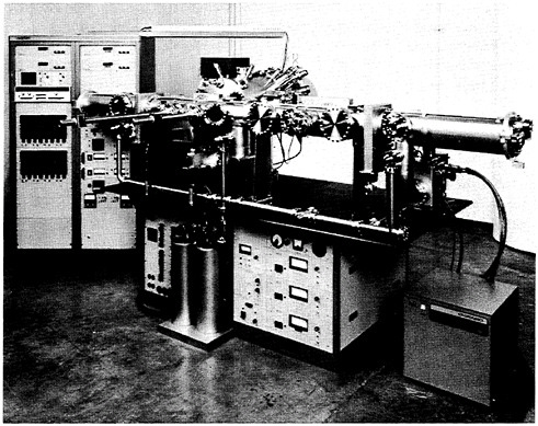
FIGURE 6.1 Molecular beam epitaxy system capable of growing thin films and multilayer structures in ultrahigh vacuum using Knudsen sources. Modular construction provides substrate loading and preparation capabilities and in situ film analysis. (Courtesy Varian Corporation.)
cally, groups in different sectors have different goals: research in industry is more oriented toward products and services, in federal laboratories toward particular missions, and in universities toward fundamental understanding. But the modes of operation in each sector are similar.
Stiff competition for research support has forced investigators to focus on short-term projects rather than risk having too little progress to report in renewal proposals. High-risk speculative research usually correlates with major advances in a field. However, results from such research, if they occur at all, often require longer to achieve than the usual 1- to 3-year funding period. If there is a long period of support without results, continuation proposals refereed by peer groups are likely to receive low marks, leading to reduced levels or loss of support. Difficult and unconventional interdisciplinary research, which is especially important in materials science and engineering, has suffered in this atmosphere.
An important function of the federal agencies, and the principal mission
of NSF, is to sustain truly innovative research. Projects supported by NSF, especially, should be expected to delve deeply and to take risks, which means that priority must be given to support for innovative individuals rather than large projects.
Research in engineering has become a proper part of the responsibility of NSF, because solving many of today’s most important technological problems requires new ideas and a thorough understanding of basic principles. However, in the face of pressing national needs, NSF may be asked to adopt too narrow an interpretation of its mission in engineering—that of searching for short-term solutions by whatever means are available rather than probing deeply to develop fundamentally new technologies. What is needed is a farsighted, interdisciplinary approach to the whole of materials science and engineering.
Collaborative Centers
The question of whether a materials-related center of excellence is beneficial depends on the circumstances involved. The center concept can be most beneficial if it provides a mechanism for several parts of the technical infrastructure to come together, so that center activities amount to more than the sum of its parts. If industrial input is factored into the work, the R&D will have a natural outlet in industrial manufacturing. The training of students and research scientists can often be combined in such an endeavor.
The United States has made three major efforts in center development in the past four decades, and each one has been successful in its own way. The 1940s primarily saw the establishment of major centers (now known as national laboratories) related to nuclear development and high-energy physics. They were established by what was then called the Atomic Energy Commission, and they now belong to DOE. To a large extent, these centers were built around major facilities—for example, nuclear reactors, accelerators, and synchrotron light sources. With them have come major efforts in materials science and engineering to use these facilities for fundamental research and for the development of materials for defense systems, civilian power reactors, and energy systems of many different types. These national laboratories are largely multipurpose, and, increasingly now, they work closely with industry in applied research. The principal point, however, is that the centers were usually built around large and expensive devices that only the federal government could afford, because the projects undertaken were too large and too expensive to be built by industry or universities.
The second group of centers, called the materials research laboratories, was established in the early 1960s in response to the recognition that materials science and engineering was becoming an interdisciplinary field drawing on chemistry, physics, metallurgy, ceramics, and engineering, as well as in
response to the belief that the development of many advanced technologies is hampered by the lack of advanced materials. (For a recent history of the origin and progress of these centers, see papers by R.Sproull and L.Schwartz in Advancing Materials Research, National Academy Press, Washington, D.C., 1987.) These laboratories, about a dozen in number, were established at major universities by the Defense Advanced Research Projects Agency of DOD, and they brought together different disciplines in an interdisciplinary facility. In 1972, administration of these laboratories was transferred to NSF. Their purpose can perhaps be summarized best by quoting from the government contracts that established the centers within the universities:
The contractor shall establish an interdisciplinary materials research program and shall furnish the necessary personnel and facilities for the conduct of research in the science of materials with the objective of furthering the understanding of the factors which influence the properties of materials and the fundamental relationships which exist between composition and structure and the behavior of materials.
The reasons for the success of these laboratories were summarized by Sproull, and a few are abstracted here from his paper:
The important features at each university were, first, that an umbrella contract provided for continuity of support and for the ability to buy large quanta of equipment and facilities. Second, a local director committed a substantial fraction of his career to making the program succeed. He would use the longevity of support to extract concessions from the university and departmental administrations. Third, the contract provided, in most cases, reimbursement over 10 years for the new construction required to do modern experimentation on materials. Fourth, the longevity of the contract induced the university to allocate the project scarce and prime space in the middle of the campus, thereby establishing the maximum informal connections among disciplines. Fifth, central experimental facilities (such as those for electron microscopy or crystal growth) could have state-of-the-art equipment, even if it was very expensive, and they served as a mixing ground for students and faculty from several disciplines. Sixth, an executive committee composed of people with power and influence in the individual disciplines but oriented toward the success of the program helped the director over the rough spots with department chairmen, people who often were overly protective of their own turf. Seventh, a contract was not given to an institution unless it had a strong disciplinary base on which to build. Eighth, individual grants and contracts with federal agencies continued; most well-established principal investigators received the majority of their support from some other agency and might enjoy help from the program only in the central facilities or the building space (R. Sproull, Advancing Materials Research, National Academy Press, Washington, D.C., 1987, p. 31).
The most recent U.S. experience in the development of centers involves the engineering research centers established by NSF beginning in 1985. These centers were formed as a new approach to meeting the serious challenges to U.S. industrial competitiveness. They are located at universities and bring together the capabilities and resources of government, universities, and in-
dustry. At cross-disciplinary engineering centers, researchers work on problems that are of technological importance to industry, as contrasted with the work done at the materials research laboratories, which specialize in the generation of scientific knowledge. The centers are formed around specific technological areas, and their titles indicate the specificity of the objective of each center: Systems Research, Intelligent Manufacturing Systems, Robotic Systems in Microelectronics, Composites Manufacturing Science and Engineering, Telecommunications Research, Biotechnology Process Engineering, Advanced Combustion, Engineering Design, Compound Semiconductor Microelectronics, Advanced Technology for Large Structural Systems, and Net Shape Manufacturing. It is planned that several additional centers will be formed in subsequent years.
Paralleling the various NSF centers in many respects, the university research initiatives sponsored by DOD were begun in FY 1986. To date, more than 91 initiatives have been funded at universities at a total cost of more than $100 million. The University Research Initiative Program includes fellowships, young investigator awards, exchange scientists, and research instrumentation funding.
The various interdisciplinary research centers supported by federal agencies in collaboration with universities and industry have made valuable contributions to materials science and engineering, and the committee believes that they must continue in the roles that they have served. At the same time, the committee believes that stronger efforts should be made to link science and engineering in interdisciplinary research centers.
FEDERAL LABORATORIES
There are more than 700 small and large federal laboratories supported by 14 federal agencies. Of this total, about 160 federally operated laboratories and about 30 contractor-operated laboratories employ 50 or more scientific and technical personnel.
Based on a survey conducted by the committee, the committee estimates that approximately 2000 people at the national laboratories work in materials science and engineering, divided about equally between the defense and nondefense laboratories.
Department of Energy Laboratories
The national laboratories funded by DOE, with their extensive technical resources and special facilities, are especially well positioned to make major contributions to materials science and engineering, as noted in Chapter 5.
The national laboratories have a long history of involvement in materials synthesis and processing, materials characterization, equipment and instrument development, and systems integration. They also have a history of organizing, operating, and maintaining major collaborative research centers and user facilities for participatory R&D by industries and universities. In general, they have much experience in bringing together multiple disciplines to solve complex problems and in overcoming problems of technology transfer between diverse institutions. However, appropriate incentives need to be developed to help these laboratories reach their full potential for collaboration with industry and universities.
Department of Defense Laboratories
There are 81 DOD laboratories supported through the Navy, Air Force, and Army, with about 90,000 staff members and a total budget of about $1.7 billion—half of the total federal laboratory budget. The property and equipment assets of these DOD laboratories are in excess of $4 billion.
Materials science and engineering is also conducted in about 124 industrial laboratories under the IR&D programs, which are reimbursed by DOD through indirect cost accounts. About 1080 IR&D projects address materials science and engineering issues, and 417 of these have materials science and engineering as their principal subject. The total amount of funding for these projects was approximately $255 million in FY1986.
National Institute of Standards and Technology
The National Institute of Standards and Technology (NIST; formerly the National Bureau of Standards), which receives its funding from DOC rather than DOE, is another potentially valuable resource for materials science and engineering. The approximate budget for materials science and engineering in the NIST in 1986 was $37.8 million, with emphases across the full range of materials classes. The number of full-time equivalent NIST staff members now working in the field is approximately 400; about 200 have doctorates.
Industrial-academic interaction is an important element of the research program at the NIST. The visiting scientist program includes a unique industrial research associate program in which industry sends personnel at its own cost to work collaboratively on joint projects with researchers at the institute, for periods ranging from a few weeks to more than a year. An estimated 20 percent of NIST operating funds comes from industrial sources, mostly via contributions of equipment or the paid time of industrial research associates.
MAJOR NATIONAL FACILITIES
In materials science and engineering, the large-scale national facilities in use today evolved gradually. The first of them, research reactors for neutron scattering, were not even built as materials research facilities but were constructed with funds designated for reactor development. Several synchrotron radiation facilities were originally high-energy physics machines. Thus materials scientists and engineers became accustomed to borrowing time on machines originally dedicated to other purposes.
Beginning in the mid-1970s, the use of synchrotron radiation in materials science and engineering expanded dramatically from an estimated 200 users in the United States in 1976 to close to 2000 users in 1986. The average annual growth rate of published scientific articles based on synchrotron radiation during that period was 30 percent. In coming years, the use of synchrotron radiation facilities will continue to evolve beyond exploration of the frontiers of materials science into more applied efforts. As industrial and governmental use of these facilities matures, an increasing amount of proprietary work will be done at synchrotron radiation facilities. Areas of potential application span a wide range of technologies related to the economy, defense, and health. For example, synchrotron radiation is a potential technology for lithography of semiconductor circuits with submicron feature sizes. It is also associated with the development of the free-electron laser, which has applications in national defense. It has applications in biological imaging. Research on synchrotron radiation will continue to focus on generating increasingly coherent sources of radiation, so that aspects of a laserlike source can be achieved from the ultraviolet to the x-ray region.
The neutron scattering community in the United States has undergone a similarly rapid increase in recent years, having doubled in just 6 years. This upsurge of users from government, industry, and universities is part of a worldwide trend; for example, the neutron scattering community in Western Europe more than tripled during the 1970s. A result will be an increasing demand for use of major facilities.
All of the major national facilities now in operation are open to users. The facility at Brookhaven National Laboratory, for example, still functions as a small science facility, despite the large number of users. Participating research teams, including teams from government laboratories, corporations, and universities, are allowed to organize and carry out their own experiments. One advantage of this arrangement is that industry invests in the instrumentation for research. Another advantage is that many of the universities with materials research laboratories have established beam lines at the facility as part of their funding for the laboratory. This arrangement allows Brookhaven National Laboratory to function in effect as a collection of many different small facilities doing many different types of science.
Thus advanced instrumentation is playing a role of growing importance in materials science and engineering research. This trend justifies the dedication of major facilities to work in the field. A 1984 National Research Council report entitled Major Facilities for Materials Research and Related Disciplines (National Academy Press, Washington, D.C.) provides detailed justification for such facilities. That report also reviewed the status of major facilities in the United States and established priorities for future facilities providing instrumentation in synchrotron radiation, neutron scattering, and high magnetic fields. Before laying out its priorities, however, the report highlighted two major recommendations: (1) resources should be provided to operate existing user facilities productively, and (2) the support of major facilities should be accompanied by expanded support of smaller materials research programs.
The priorities established by the National Research Council’s Major Materials Facilities Committee were construction of major new facilities and establishment of new capabilities at existing facilities. Assessing only facilities with an initial cost of at least $5 million, the committee recommended construction of (1) a 6- to 7-GeV synchrotron radiation facility, (2) an advanced steady-state neutron facility, (3) a 1- to 2-GeV synchrotron radiation facility, and (4) a high-intensity pulsed neutron facility. With regard to new capabilities at existing facilities, the committee recommended (1) centers for cold neutron research, (2) insertion devices on existing synchrotron radiation facilities, (3) an experimental hall and instrumentation at Los Alamos National Laboratory, (4) upgrading of the National Magnet Laboratory, and (5) enriched pulsed neutron targets.
This committee concurs with the earlier prioritization of major national facilities, and it notes with approval that construction of several of them has recently been started. Current plans call for the construction of the 6-GeV synchrotron radiation facility at Argonne National Laboratory, with the lower-energy machine being built at Lawrence Berkeley Laboratory. According to the most optimistic scenarios, neither of these facilities is expected to be operational before the early 1990s. Part of the experimental floor of the National Synchrotron Light Source is shown in Figure 6.2. Implementation of the highest-priority recommendation for upgrading existing facilities—to build new cold sources, guide halls, and instruments at Brookhaven and NIST—has begun at NIST and when completed will greatly enhance the capabilities of that facility.
The second-priority recommendation in the area of major new facilities and noted aims is for an advanced steady-state neutron facility. This recommendation needs to be fully implemented. There are major opportunities in materials science and engineering if higher fluxes and advanced instruments become available. The increased sensitivity and resolution will greatly extend the range of sizes and level of microstructural features that can be
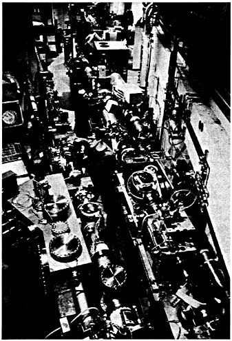
FIGURE 6.2 Shown are two pairs of beams lines coming from the high-energy x-ray storage ring at the National Synchrotron Light Source that are dedicated to materials science. They were constructed by the Naval Research Laboratory and the National Institute of Standards and Technology. On the left pair of lines, x-ray tomography and scattering experiments are performed. On the right pair, soft x-ray spectroscopy and photoemission experiments are performed. (Courtesy Brookhaven National Laboratory.)
studied in bulk materials. It will be possible to follow the kinetics of processes such as precipitation, phase decomposition, coarsening, and damage accumulation in real time. These advanced capabilities for microstructural and nanostructural research and evaluation will provide important fundamental information directly related to the processing, behavior, and reliability of advanced materials.
FINDINGS
Many in the materials field believe deeply that the United States has a critical need for wholly different types of major national facilities, that the country needs facilities that concentrate directly on problems of industrial importance in ways that can help U.S. materials-related industries gain or maintain a competitive edge in the international arena.
A number of state initiatives aim to address this problem. But at the national level the United States has nothing of the scope of the Fraunhofer institutes in West Germany or the quite different Japanese initiatives in the materials field. In 1988 alone, for example, Japan initiated two major new research consortia in the materials field. One of these, in the field of superconductivity, has funding commitments of approximately $26 million per year for 10 years. (This figure does not include the salaries of the estimated 100 researchers to be involved.) The second initiative is in the field of forming of semisolid metals and composites. It is funded at about $30 million for 5 to 7 years (again excluding salaries of researchers).
Modern advanced materials almost invariably require the most sophisticated synthesis and processing facilities. For example, electronic materials such as semiconductor crystals, epitaxial layers, fabricated chips, and optical fibers frequently must meet impurity requirements at the sub-parts-per-billion level to be useful for fundamental studies or applications. Consequently, clean rooms are now a normal requirement for any serious research capability in electronic materials. Typical clean-room costs are in the range of $100,000 to $1 million depending on size and class. Chip fabrication facilities, now a normal requirement for teaching and university device research, are even more expensive. Preparation of many electronic materials requires extremely poisonous reagents. For example, III–V semiconductors often require arsine and metallo-organics that are 10 times more lethal than hydrogen cyanide. A typical laboratory preparative facility for arsine use costs from $100,000 to $1 million.
Molecular beam epitaxy (MBE) gives a finesse in preparation unequaled by any other technique. Control is literally at the atomic level. Novel structures exhibiting new quantum physics can be prepared. Novel devices have been fabricated. Future possibilities, especially those beyond the III–V semiconductors in which most of the work to date has taken place, are just
beginning to be realized. However, MBE equipment is not cheap. Again, the range is $100,000 to $1 million for an “entry-level” apparatus. Once an MBE apparatus has been used for a particular class of materials, it cannot be readily converted to the preparation of unrelated materials because of the very high levels of purity required for MBE materials.
Similar expenses are encountered for high-pressure equipment for modern synthesis, for the preparation of modern ceramics, and for polymer processing facilities, among others. Even Czochralski crystal-pulling equipment typically costs more than $1000 per station, and production-size equipment, which is sometimes necessary to study factory conditions realistically, can be 100 times more expensive.
Similar examples related to other materials classes can readily be cited. For example, clean rooms for processing modern ceramics are critical at a number of stages to minimize flaw formation. This and other equipment costs (e.g., for sol-gel and laser synthesis, attrition, and hot isostatic pressing) can readily total in the range of $5 million to $10 million for a sizable laboratory. For metal processing research, rapid solidification equipment, vacuum melting and deformation equipment, and advanced instrumentation for in situ process analysis rapidly bring costs to a similar range.
Understanding of materials at the atomic through the macroscopic levels constitutes the technological base for most modern manufacturing. Only for the most rudimentary operations in manufacturing (e.g., assembly of completed parts), is it possible to control yield, quality, cost, and schedule without understanding, at the most basic level, the materials being processed. This is certainly the case with materials synthesized at the atomic or nanometer scale, but it is also increasingly the case with so-called good, old-fashioned monolithic materials.
Clearly, modern synthesis and processing are neither string and sealing wax nor beaker and Ehrlenmeyer flask activities. Synthesis and processing require substantial investment in equipment. Industrial laboratories usually realize these needs and generally support synthesis and processing activities at an appropriate level. The understanding that synthesis and processing require large expenditures in academia and government laboratories must be more widespread if materials science is to have the steady stream of trained people, new materials, and well-controlled processes that are essential for realization of its potential.
The committee, therefore, recommends substantially increased expenditures on facilities for synthesis and processing research in universities and other laboratories—for use by individual investigators and small groups of investigators. It also recommends establishment of major national centers for synthesis and processing, involving universities, industry, and government. Such centers could be expected to focus on generic synthesis and processing, or on a given materials class. Some would also be expected to
have an advanced instrumentation component (e.g., synchrotron light sources for semiconductor processing). Some would be expected to involve close coordination with disciplines outside the materials or materials-related fields (e.g., business). All would focus on development of industrially useful technology, technology transfer, and quality and economy in design and production processes.


