
INFORMATION AND COMMUNICATIONS
Information procurement, management, and movement occupy a central position in our modern world. Chemistry and chemical engineering play a significant or even enabling role in the majority of information and communication technologies that support an industry that collects, processes, displays, stores, retrieves, and transmits vast quantities of digital data. Such activities require electronic microcircuits, lightwave
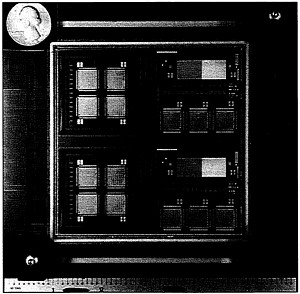
The first transistors (inset) assembled in 1947 led to revolutionary developments in the electronics industry and changes in our way of life. The original transistor is compared here with a prototype 64-megabyte wafer.
communication systems, magnetic and optical data storage, advanced packaging, and optical interconnection, to name just a few of the key technologies involved.
Progress and international competitiveness in these technologies depend on a strong fundamental science and engineering infrastructure. Advances must be made not only in understanding the underlying phenomena and materials, but also in translating scientific advances into functional products of high performance, high quality, and competitive cost.
Optical Fibers
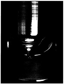
Since becoming a commercial reality in the early 1980s, optical fibers have almost completely replaced copper wire in the long-range transmission of data and voice. The data-transmitting capacity of optical fiber systems has doubled every year since 1976, and the optical fiber industry now generates annual revenues of over $2 billion. Sometimes known as photonics, this technology utilizes wavelengths of light that are not absorbed by the glass fiber to transmit signals for telecommunications, data and image transmission, energy transmission, sensing, display, and signal processing. The effective propagation of light along an optical fiber is made possible by a core that has a higher refractive index than the cladding. The core is produced by doping pure glass with oxides of phosphorus, germanium, or aluminum, and the cladding consists of pure silica glass or silica doped with fluorides or boron oxide.

A “gob” falls from the heated end of a pure silica blank, to be drawn into an optical fiber.
Several processes are used to manufacture the glass body from which an optical fiber is drawn. One example is modified chemical vapor deposition (MCVD), in which chemicals flowing through a glass tube produce a deposit on the interior wall when the outside of the tube is heated by a flame. More than 100 layers with different refractive indices can be deposited, and when deposition is complete, further heating collapses the tube to form a glass rod. Glass rods formed in this way are drawn into a thin fiber and coated with a polymer to protect the fiber surface from microscopic scratches and moisture that would seriously degrade fiber strength.

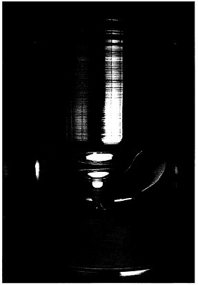
Hair-thin fibers of ultrapure glass are now used to transmit voice, data, and video communications in the form of digital signals emitted by semiconductor lasers.
Optical fibers are currently much more expensive than commodity glass because of the exquisite precision and control required for their manufacture. Consequently they are limited in both availability and cost-competitiveness. Glass fiber manufacture lends itself to automation, and continued chemical and chemical engineering research could someday allow a fiber manufacturing plant to move continuously from purification of chemical reagents through a series of chemical reactions and finally to glass-forming and fiber-drawing operations. Intermediate products would never have to be removed from the production line, and the cost of glass fiber could be reduced by as much as a factor of 10.
Nanofabrication
Microelectronic device fabrication begins today with the growth of ultrapure silicon single crystals as large as 8 inches in diameter and 5 feet in length. These single-crystal ingots are subsequently cut into wafers that are polished to a high degree of smoothness. The wafers next enter the lithographic process, first being covered with a thin insulating film and next coated with an organic material known as a photoresist that undergoes a chemical transformation upon exposure to light. Careful exposure of the selected parts of the photoresist to light projected through a mask allows either the exposed or the unexposed portion of the resist to be selectively dissolved, leading to a relief image. The remaining portion of the resist
Streamline patterns in a chemical vapor deposition (CVD) reactor employed for the production of solid-state electronic components.
shields the underlying silicon while other parts of the wafer are subjected to further chemical reactions. A series of such steps produces an integrated circuit pattern on the silicon. The resulting chips, each only a few square centimeters in area, may contain as many as 20 layers of semiconductor, dielectric, and conducting films. The individual features currently have dimensions as small as 0.5 micron.
A single-crystal silicon ingot used in the preparation of silicon wafers for microelectronic device fabrication.
Greater levels of integration have been achieved over time by decreasing the size of the individual circuit features, particularly through the use of ever-shorter wavelengths of light; the minimum feature size obtainable in a photoresist pattern is directly proportional to the wavelength of the exposing radiation. By the end of the decade, optical exposure may yield to the very short wavelengths of x-ray irradiation, but totally new photoresist materials will be required. Each new generation of photoresists requires extensive chemical research to optimize for the specific wavelength of light to be used in the lithography process, and scale-up to manufacturing quantity by chemical engineers.
An even more profound shift is occurring in lithographic processing. Current technologies rely on changes in solubility of the photoresist when exposed to light. Future integrated circuit production will require dry processing techniques that are compatible with all-vacuum manufacturing systems. One approach to etching will be the use of a radio-frequency or microwave plasma, produced by ionizing an appropriate gas with a high-energy oscillating electric field. The future development of plasma-assisted processes depends heavily on basic research in chemistry and chemical engineering, both in designing the necessary chemical processes and in developing process control methods and sophisticated reactors to ensure manufacture with high yields at the lowest possible costs.
The importance of chemistry and chemical engineering does not end with the formation of the lithographic image. Selective implantation of the silicon substrate with arsenic or boron species is used to produce the desired electrical properties, and subsequent deposition steps make the necessary wiring. Improved metallization and deposition techniques will be essential to the next generation of devices. An even greater change, but one
that is now in a much earlier stage of research, is the replacement of silicon by materials such as gallium arsenide for the fundamental building block for integrated circuits; gallium arsenide devices are capable of much faster performance than are those fabricated from silicon.
Electronic Packaging
In the microelectronics industry the term packaging denotes those components in a system that interconnect and support the semiconductor logic and memory chips. The package carries electrical signals between chips, distributes electrical power to the chips, dissipates heat, provides mechanical support, and protects the chips and circuitry from physical or environmental damage. Packaging components can be as simple as a molded plastic chip-carrier box or as complex as the multichip modules found in today's high-speed supercomputers.
Plastic electronic packaging, now a mature and reliable technology, dominates high-volume applications such as consumer electronics. An organic polymer is molded around the actual chip, providing a protective shell that also anchors the wires or pins for electrical connections. The polymer must have good chemical and mechanical stability, including the ability to withstand typical soldering temperatures. The encapsulated chip is then soldered to a printed circuit board, which provides power distribution and electrical interconnections. Circuit boards can contain more than 30 precisely aligned layers, each having carefully constructed interconnection circuits.
Complex ceramic structures are the chip carriers of choice for most high-end applications. Multichip modules are prepared from ceramic precursor particles that are first cast into a thin film using an organic polymer binder. Patterns of metal particles are applied to the film in a process similar to silk-screening. The individual layers are then aligned and fused together at elevated temperatures to form the final ceramic and embedded metal circuitry. The ceramic multichip module in the heart of a modern mainframe computer may be 5 inches square with more than 60 individually prepared layers that were fired together to form a final monolithic package that supports as many as 121 chips. At present, the complex process is as much an art as a science, and considerable research on materials and chemical processing techniques will be
The world's largest aluminum nitride (AIN) multichip module, this package is made up of two silicon-based, high-density multichip interconnects inside a 4 inch by 4 inch cofired AIN package. The module is capable of dissipating over 40 watts and can operate at clock speeds of up to 348 megahertz.
required if these substrates are ever to find application and be competitive in lower-cost, larger-volume applications.
Overall system performance in high-end computers is now increasingly limited by the speed with which signals can be transmitted from chip to chip. One approach to overcoming this bottleneck is the use of chip carriers made of materials with lower dielectric constants than those of even the best ceramics. Several manufacturers have already introduced carriers in which a polymer layer on top of the ceramic carries the most critical wiring. The materials of choice have been polyimides, which exhibit excellent mechanical and thermal stability in addition to a low dielectric constant. On the other hand, the difference in the thermal expansion properties of the available polyimides and the ceramic can result in substantial stress and the ultimate failure of the device; chemists must therefore develop new polyimides, if not entirely new classes of polymers, to meet the challenges of this application.
Heat dissipation has become one of the most formidable problems in electronic packaging. The chips in today's high-end computers may produce heat at the rate of 60 watts per square inch. Yet the semiconductor chip must be maintained below a permissible operating temperature, typically less than 175 degrees Fahrenheit. Computer manufacturers have used water cooling or immersion of the circuits in a temperature-controlled liquid fluorocarbon. But future, more powerful machines will depend upon research by chemical and mechanical engineers to develop better methods for heat dissipation. These may include the utilization of advanced ceramic materials such as aluminum nitride, a material with a combination of excellent thermal and dielectric properties; this material will require processing techniques such as hot pressing, which will permit large device sizes with high dimensional accuracy.
Optical Interconnection and Optoelectronic Devices
A striking trend in information processing is the increasing replacement of the current electronic devices and systems with hybrids known as optoelectronic devices or optically interconnected systems; at the extreme are photonic devices, which are purely light-based. Fiber-optic cables are finding increasing use for high-speed communication among computer processors and associated devices. Optical communication supports the transmission of large amounts of data with substantial immunity from the electronic noise that can interfere with wire-based communication: two beams of light can actually cross one another without interfering with the information content in either.
New applications of optoelectronics are likely to include high-speed communication between printed circuit boards and even between chips. Hybrid systems with discrete optical and electronic components will eventually be replaced by integrated devices containing both optical and electronic elements, which are manufactured by processes comparable to those used to manufacture modern integrated circuits. For this to be possible, new materials for conducting light signals will need to be developed.
The next opportunity for performance enhancement lies in the replacement of the electronic switching devices for the routing of information in computer systems. Most likely this advance will use optoelectronic switches that may function by absorbing and reemitting light rather than just by transmitting it; this technology relies on the nonlinear optical properties of materials. Recent research indicates that good nonlinear optical properties can be obtained by incorporating certain chemical groups in organic polymers, aligning the groups in a strong external electric field, and then cross-linking the polymer to form a rigid three-dimensional structure. This approach is particularly attractive because polymer fabrication is a well-developed technology, but research chemists must learn how to circumvent such serious problems as the decay of nonlinear optical properties with device age.
The all-optical computer, in which the actual digital processing will be done by optical rather than electronic devices, lies farther in the future. However, optoelectronic devices may become useful in the near term for recording and retrieval of information. When light passes through certain nonlinear optical materials, it undergoes frequency doubling. Because information density on optical recording media is proportional to the frequency of the light used, nonlinear optical materials could significantly enhance the storage of information on optical media. Someday even greater enhancements might be possible through the technique of holographic storage, which could allow multiple pieces of data to be stored in the same physical space within a nonlinear optical material.
Display Technologies
Dramatic improvements have been made in computer display technology in recent years. But even a high-resolution color graphics screen uses the basic technology of the cathode ray tube (CRT) that has been familiar to television viewers for decades. Portable and notebook computers have become the major driving force for the development of alternative, flatscreen display technologies. These machines require thin, lightweight displays, and a major research challenge is presented by the reluctance of users to give up the full color and high resolution of existing desktop systems.
One rapidly evolving display technology is based on materials known as liquid crystals. Typically, liquid crystals are organic chemicals that can form a state that is intermediate between the random order of a true liquid and the highly ordered molecular arrays of a crystalline solid. The molecules in a liquid crystal will line up in the same direction, but an external force such as an electric field can cause a change in the collective orientation of these molecules. If a system is constructed in such a way that the liquid crystals transmit light in one orientation but not in another, local electric fields can be selectively applied to generate light or dark spots. Taken together these spots generate an overall image, a phenomenon that is now widely used in digital wristwatches and automotive instrument displays.
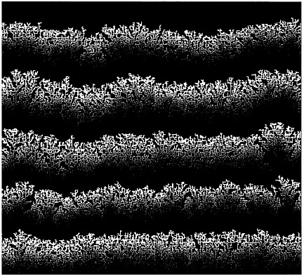
Computer simulations are used in research on the growth of thin films formed by chemical vapor deposition. The growth model predicts the fractal surface shown.
The current high point of display development, the thin-film transistor liquid crystal display (TFT-LCD), is a remarkable device in which each picture element is driven by its own individual transistor. The liquid crystals used in these displays constitute a new generation of high-switching-speed materials specifically synthesized for this application. Full-color high-resolution TFT-LCDs, now found in the most advanced notebook computers, provide exceptional performance, even against the high standards of the CRT. This technology may be the forerunner of a large-screen, flat-panel television that can be hung on the wall like a painting.
The manufacture of these displays makes extremely high demands on process control. A single notebook-sized display may contain as many as 1 million thin-film transistors, every one of which must work properly: the acuity of human vision is such that even a single bad display element can be a noticeable and unacceptable defect. The narrow margin for error demands that each of the manufacturing steps be understood and controlled in great detail through extensive research on process characterization and modeling. The development of new chemical vapor deposition techniques for selective repair of defective thin-film transistors may also be necessary to enhance manufacturing yields.
Data Storage and Retrieval
A hierarchy of storage devices has arisen in the information processing industry. Semiconductor random access memory (RAM) provides high-speed retrieval and temporary storage of data as they are being processed. Direct access storage devices (DASD), traditionally disk-based magnetic storage devices, provide intermediate access speeds at significantly lower costs. Magnetic tape, the slowest and cheapest of the storage technologies, provides archival storage for data backup and maintenance of historical records. Optical recording technologies, relative newcomers to data recording and storage, currently have cost and performance characteristics intermediate between those of DASD and tape. However, optical methods have the potential to be faster, cheaper, and more reliable than magnetics.

Continuing research will lead to improved processes and materials for the production of optical disks.
The performance of magnetic tape, the most mature and least costly of these technologies, continues to improve. The tape substrate is a highly developed organic polymer, typically a polyester film, on which is coated a mixture of magnetic particles in an organic binder or glue. Because the moving tape contacts the recording head, particular emphasis has been placed on the durability of both the head and the tape materials.
Magnetic disk recording technology presents greater challenges than magnetic tape technology in both materials and process research: access speeds must be constantly increased to keep pace with performance improvements in processors. The traditional magnetic disk, a rigid aluminum alloy substrate coated with a thin layer of magnetic iron oxide dispersed in an organic binder, is rapidly being replaced by thin-film disks in which the magnetic layer is a continuous covering of a metal alloy such as cobalt-chromium. The state-of-the-art thin-film disks must be made by using vacuum deposition techniques such as sputtering or evaporation.
This requirement forces fundamental changes in processing and process control. In addition, the thin-film disks are considerably more fragile than the earlier aluminum disks, so that a very thin overcoat is necessary to provide physical protection. This overcoat is typically a hard amorphous carbon material that is formed in a vacuum deposition process.
Although the recording head actually flies above the disk rather than riding in contact with it, the separation tolerances are extremely small, and there are inevitable contacts between the head and the disk. Application of an organic lubricant to the disk surface has been found to minimize the damage from such contacts and to lengthen disk life; fluorine-containing long-chain molecules were synthesized to accomplish this difficult task.
The magnetic heads that read and record data have also undergone substantial change. Increased storage density on the disk has mandated a very small head that cannot be machined by the mechanical techniques used in the past. Head manufacturers have instead turned to the chemical fabrication techniques of the microelectronics industry. The new thin-film heads are actually produced by lithographic processes similar to those used in the manufacture of integrated circuits, although the differences are sufficient that new materials and techniques had to be developed. In the future, it is likely that the data-reading function of the thin-film magnetic head will be taken over by a magneto-resistive element, promising enhanced sensitivity but introducing an entirely new set of materials and processing challenges.
Reversible optical recording has presented its own challenges to chemists and chemical engineers. Recording is accomplished by causing changes in the reflectivity properties of a metallic alloy when it is heated by a laser in the presence of a magnetic field. Reflections from a second, much weaker laser beam allow the recorded information to be read back. Some of the best alloys for this application undergo chemical degradation in normal air and must be protected from the atmosphere. The development of inexpensive polycarbonate polymers has provided adequate protection from the atmosphere while maintaining the required optical clarity and freedom from defects. Future designs will require more advanced polymeric materials that maintain these desirable properties but allow higher disk rotation speeds without deformation.
Single-atom Manipulation
Since the development of the scanning tunneling microscope (STM) in 1986, chemists have been able to observe single atoms in a number of different environments. The ability to produce images of individual atoms at the surface has found widespread use as a characterization tool, in particular, allowing scientists to image systematic defects on single-crystal or amorphous
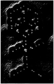
Molecular man. This image is composed of 28 individual molecules of carbon monoxide on a single-crystal platinum surface. The image was assembled by individually moving each of the molecules into position using a scanning tunneling microscope tip.
surfaces. A detailed knowledge of such defects on silicon surfaces is essential to further advances in the microelectronics industry. As the feature size of individual integrated circuit components continues to shrink, the control of these defects in the silicon substrate becomes increasingly critical in device fabrication.
Recently, scientists discovered that the STM can also be used to move individual atoms on a surface. Careful voltage control of the microscopic probe used in STM imaging permits a single atom to be picked up and subsequently deposited in a desired location. Because silicon atoms can be manipulated at the readily accessible temperature of liquid nitrogen, unprecedented control and precision may be possible in the construction of semiconductor devices. Ultimately, the ability to manipulate single atoms could lead to controlled reactions of single atoms and molecules—and to new chemicals, materials, or structures that simply could not be created by existing chemical methods.
MICROELECTRONICS FACTORY OF THE FUTURE
Many modern consumer products — calculators, digital watches, and microwave ovens — as well as advanced computers depend on microelectronics for their operation. The key to microelectronic devices is the integrated circuit, which consists of multiple layers of precisely patterned thin films, each chemically altered to achieve specific electrical characteristics. Manufacture of these devices, currently by a complex series of labor-intensive chemical and physical processes, will undergo considerable change during the next 10 years, partly to meet the challenge of international competition. Take a glimpse at a microelectronics factory in the year 2002:
The new facility is totally integrated, a mere one tenth the size of the old-style facility, and constructed at only one fifth of the cost. It produces chips with line widths of 0.15 micron or smaller at a success rate of nearly 90 percent, dramatic changes since 1992, when line widths were 0.5 micron and only 50 percent of the chips survived the manufacturing process.
The unique facility is highlighted by a modular array of equipment clusters surrounding a central processing host, a design that permits major reductions in manpower and space requirements, with correspondingly lower costs. There is greater flexibility for making a wide range of products in a single production cycle, and the ultrahigh-vacuum conditions minimize the generation and release of chemical waste. The facility has resulted from intensive research by chemists and chemical engineers in devising new materials, studying their chemistry and rates of reactions, and designing new equipment and processes.
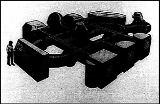
The microelectronics factory of the future. The ultrahighvacuum process is modularized to yield many advantages, as explained in the text.
This factory also uses a new operating strategy, replacing the old trial-and-error approach to equipment design and operation with process models that are based on extensive research into chemical reaction mechanisms and transport phenomena. Real-time feedback from artificial intelligence sensors provides reliable control of each processing step, and links to the factory's powerful main computer enable the downloading and modification of recipes for each wafer. The process chambers of these single-wafer systems employ short reaction times, allowing sequential processing in the same reactor and circumventing the higher capital costs of old-style multiple-reactor systems.
The intervening years of research have greatly changed the role of chemists and chemical engineers since the 1990s. The production of a new chip no longer requires years of laboratory development, and an extensive library of computer data allows a unique microelectronic device to be designed quickly. After first locating the half-dozen most promising materials, the computer carries out molecular-level simulations, producing holographic displays of the top candidates that the process engineer can “see” and “touch.” The computer then evaluates the designs for manufacturing applicability, checking such details as reactor design and likelihood of crystal defects. Finally, the computer prints out two or more alternative designs, along with their associated costs. Human judgment returns at this point, as the process engineer selects the preferred design and tells the computer to make the new chip.


