
Active Electro-Optical Component Technologies
As has been described in Chapters 2 and 3, current and emerging active electro-optical (EO) sensing systems are implemented in many different modalities. All require components such as lasers, detectors, optics, and processing techniques to generate photons, bounce them off targets, and transform detected photons into usable information. Other components may be required as well, depending on the implementation. The specific requirements, complexity and sophistication of the components vary with the manner of implementation of the active EO sensing system and the usable information it is trying to extract. For example, no particular laser or detector technology meets all the requirements of the various active EO sensing approaches. An important factor in the last ten years’ progress has been technological advances in each of the components of the active EO system: improved lasers, detectors, software, advances in robotics, and improved manufacturing technologies. This chapter discusses the variety of components currently used and some of the key technologies being developed for future systems.
Active EO sensors employ coherent sources in the wavelength region from the long-wavelength infrared (around 10 µm) to the atmospheric transmission limit for UV light, around 200 nm. The sources can be based either on lasers or on nonlinear optical systems driven by lasers. Lasers are typically categorized by the type and format of the medium used to generate their output, which at the highest level are gases, liquids, and solids.
Solid materials are further categorized by their electrical characteristics. Solid-state lasers employ insulating solids (crystals, ceramics, or glasses) with elements added (dopants) that provide the energy levels needed for laser action. Energy to excite the levels is provided by other sources of light, either conventional sources such as arc lamps or other lasers, a process called optical pumping.
Solid-state lasers in turn are divided into two broad categories, bulk or fiber, with the latter having recently emerged as an important technology for generation of high average powers with high beam quality, as discussed below.
Even though they are also made from solid-state materials, semiconductor lasers are considered to be a separate laser category. While the lasers can be made to operate by optical pumping, if the semiconductor material can be fabricated in the form of an appropriate p-doped, n-doped (PN) junction, it is possible to pass electrical current through the junction and generate laser output directly. These “diode lasers” are by far the most widely used form of semiconductor lasers, and have led to major advances in source technology for active EO sensors.
The use of lasers for active EO sensors started with the use of the first laser to be operated (1960), the solid-state ruby laser.1 With the development of techniques to generate nanosecond-duration pulses, ruby lasers provided the first example of laser rangefinders. Since 1960, almost every type of laser has been employed in demonstrations of active EO sensors. At this point, with a few exceptions, sensors now
____________________
1 T.H. Maiman, 1960, “Stimulated optical radiation in ruby” Nature 187(4736): 493.
employ either diode or solid-state lasers, with the latter often combined with nonlinear optics. This looks to be the case for the foreseeable future, owing to a favorable combination of output format, operating wavelength, relatively high efficiency, ruggedness, compact size, and reliability.
With regard to nonlinear optics, most systems employ crystals with special properties that can convert a laser output to shorter wavelengths by harmonic conversion or to longer wavelengths, by parametric processes. The latter have the added advantage that the wavelengths generated can be tuned by a variety of techniques, an advantage for sensors that require specific wavelengths—for example, in the detection of specific gases. In some cases parametric and harmonic processes can be combined for added wavelength tuning.
The next sections go into more detail regarding the dominant active EO sensor source technologies. A reasonable amount of space is devoted to diode lasers, because they now feature prominently as both stand-alone devices for low-cost, short-range sensors and as optical pumps for solidstate lasers used for long-range sensors.
Diode Lasers
There are two major types of diode lasers, interband and cascade. The former is by far the most widespread in use, but the recently developed cascade lasers have emerged as an important source of mid- and long-wave infrared emission.
Diode Lasers: Interband, Edge-Emitting
Interband diode lasers employ electronic transitions between energy states in the conduction band and the valence band of the semiconductor crystal. First and foremost, the semiconductor material used for the diode laser must have a direct optical bandgap—that is, the electronic transitions giving rise to laser operation must occur without the assistance of mechanical vibrations (phonons) in the semiconductor. This eliminates the most common semiconductor material, silicon, as well as the related material germanium.
Laser operation in direct-bandgap semiconductors occurs by optical transitions between the lowest-lying electronic states in the conduction band to the highest-lying states in the valence band, with the requirement that there be a higher density of states occupied in the conduction band than in the valence band. This nonequilibrium condition, or “population inversion,” occurs in diode lasers through the injection of sufficient electrical current into the lasing region.
Fabrication of a diode laser (Figure 4-1 for an edge-emitting device) requires that the semiconductor material be available in both n-type (electrons the majority current carrier) and p-type (holes the majority current carrier), with this achieved by the addition of certain impurities to the materials. While there are many semiconductors with direct bandgaps, many of these, for a variety of reasons, cannot be doped to make both n- and p-type materials to form diodes, notably all of the so-called II-VI binary semiconductors such as CdS, CdTe, ZnS, ZnO, and ZnSe. (The Roman numerals refer to the relative positions of the elements in the periodic table.) Infrared lasers have been operated based on IV-VI materials such as PbS and PbSe but require cryogenic cooling for efficient operation. To date, III-V binary, direct-bandgap semiconductors such as GaAs, GaSb, InAs, InSb and, most recently, GaN, as well as alloys of these crystals with other III-V elements, are by far the most widely used materials for use as diode lasers. Noncryogenic operation in the 350-2,000-nm region is possible with devices based on III-V materials.
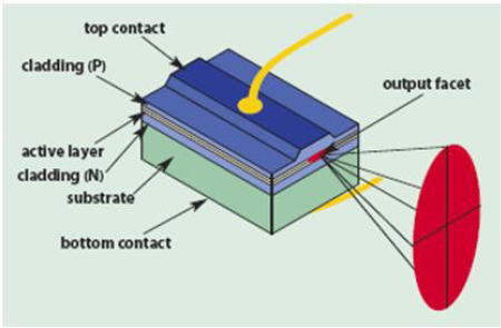
FIGURE 4-1 Reprinted with permission from The Photonics Handbook, online at http://www.PhotonicsHandbook.com. Copyright 2013. Laurin Publishing, Pittsfield, Mass.
Figure 4-1, though a very simplified diagram, shows the key features, of an edge-emitting interband diode laser. Electrical current passes through a wire bond to a stripe top contact, which confines the current in two dimensions. In the device shown, the current passes (is “injected”) through p-type material into the “active layer,” fundamentally a junction between p- and n-type material, then through n-type material to an electrical contact to complete the circuit. Laser gain occurs in a thin, 3-D region comprising the active layer, with the third dimension set primarily by the width of the stripe contact. The injected current and the structure of the device act to form an optical waveguide that confines the laser light to the same region as the gain, both vertically (perpendicular to the plane of the junction) and horizontally (parallel to the junction plane.) Most edge-emitting diode lasers operate with the laser cavity formed by the cleaved ends of the waveguide region. One end is coated with a deposited stack of dielectrics to form a highly reflecting mirror, while the other end is coated to provide only a small amount of reflectivity. Typical lengths between the two faces are in the sub-to several-millimeter range. In some cases one diode end has an antireflection coating to enable use of an external mirror and/or tuning element to obtain more control of the diode wavelength.
In reality, the details of the junction are much more complex than the simple PN junction implied by Figure 4-1. Major developments in diode-laser performance, from the first demonstrations of operation in the early 1960s, have been the result of developing the fabrication technology to make multilayer semiconductor structures (heterostructures) that better confine the lasing region and reduce the current needed to get laser operation, as well as increase the efficiency in converting electrical power to laser power. As the thickness of the layers has been reduced with improved processes to tens of nanometers, quantum effects that fundamentally change the nature of the semiconductor-material energy levels have been utilized to further improve performance. In addition to structuring in the plane of the junction, additional material structuring in the horizontal direction to confine the current and laser power has led to better laser properties.
A critical and fundamental characteristic of a diode is the nature of the region where laser action occurs. Referring to Figure 4-1, in the vertical direction the region of laser emission is limited to a dimension of about 0.5 µm, set by the fundamental nature of the junction. This is comparable to or smaller than the wavelength of the light emitted, which assures that the light (“fast axis”) emitted in the vertical direction is diffraction limited, consisting of only a single transverse mode. In Figure 4-1 the beam dimension is larger in the vertical direction because the fast-axis light rapidly diverges from the
small emitting region. To effectively capture all of the power from the diode laser requires fast optics, at least for the fast-axis light, and this is accomplished with specialized aspheric optics, often fastened directly to the diode-laser package.
The limiting feature of the small dimension is that even relatively low absolute power levels lead to very high power densities at the surface of the edge-emitting diode laser, on the order of 10 MW/cm2, and can lead to catastrophic optical destruction (COD) of the diode laser beyond certain power levels. COD results from the inevitable defects at the surfaces of semiconductors, which absorb the laser light, heat up, and, with enough power, melt the material at the surface. Means to improve the COD level are often considered proprietary or, at a minimum, patentable, by the diode manufacturers. For some semiconductor materials, particularly compounds designed to operate at wavelengths of 1,500 nm and longer, the diode power levels are limited by simple heating effects, well below the levels set by COD.
No matter the cause of the limited power, one can increase the power output of an edge-emitting diode laser by increasing the width of the lasing region along the horizontal direction, which reduces the intensity at the surface for a given absolute power level and also the generated heat density. Unfortunately, beyond a dimension of several microns, the light emitted in the direction along the plane of the junction becomes multimode. State-of-the-art diode lasers are able to generate diffraction-limited continuous wave (CW) powers on the order of 0.1 W/µm of horizontal width, so that diode lasers with strictly single-mode outputs are capable of only 0.1-0.2 W of output power. The low power is adequate for many applications, and for optical data storage devices (CDs, DVDs and Blue-Ray discs) the yearly volume of low-power diode lasers approaches 1 billion.
An upper limit to the power from a single emitting region is found when the laser action, rather than occurring through the cavity formed by the cleave ends, starts in a perpendicular direction along the width of the stripe. Typical junction widths for so-called broad-stripe lasers are in the 100-400µm range. State-of-the-art diode lasers operating in the 900-nm wavelength region can generate 10-15 W of CW power with a 100 µm stripe width.
In order to produce diode lasers with higher average power, the semiconductor laser industry, starting in the 1980s, took advantage of improvements in material quality and lithographic techniques to manufacture multiple diode lasers on one piece (“chip”) of semiconductor material.
Figure 4-2 is a schematic of a multi-emitter diode “bar,” and the most common overall horizontal dimension is 1 cm. The bar fabrication requires a means to suppress laser action along the length of the bar, and an additional manufacturing challenge is mounting the bar on a heat sink to remove the heat efficiently while also keeping the entire bar in one plane, so all of the emitters line up exactly. If they do not, the net divergence of all of the beams after collection by external optics increases. Key bar parameters are the number of emitters per bar and the stripe width of each emitter, leading to the “fill factor” for the bar, with typical stripe widths in the 100-200µm range. Unlike single-emitters, the power output of bars running in the CW mode is thermally limited, although recent improved thermal engineering of bar mounts and cooling may lead to COD starting to become a limit as well. The thermal limits to power can be overcome if the diodes are run in pulsed mode, sometimes referred to as quasi-CW (QCW). Typically, this mode is used for pumping solid-state lasers, with pulsewidths and on-time (duty cycle) percentages in the 0.1-1-msec and 1-10 percent ranges.
Present state-of-the art bars, designed for CW operation, have fill factors of 30-50 percent, and for the most efficient semiconductor materials, operating in the 900-nm region (“9xx devices”), commercially available power levels are as high as 160 W. Higher powers are possible with reduced device lifetimes, which drop rapidly as the temperature of the semiconductor junction increases. QCW bars run with fill factors of 75-90 percent and peak power levels of 250-300 W for 9xx devices.
Appendix C provides a number of tables that review the state of the art today in lasers. Table C-1 summarizes the key features of edge-emitting diode lasers, in both single-emitter and bar format. Given the significance of such devices for a number of commercial and military applications, there is continuing development of devices over the entire spectral range, and the performance (power, efficiency) and, to a lesser extent, the wavelength coverage can be expected to improve in the next 10-15 years.
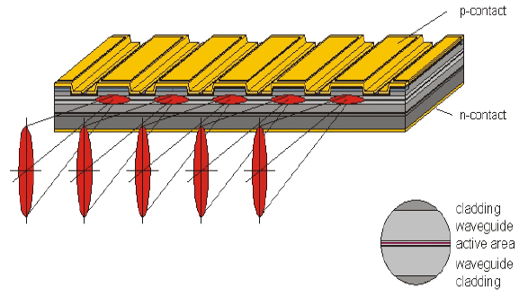
FIGURE 4-2 Diagram of “bar” lasers. SOURCE: © Jeniptik Laser GmbH.
The specific configurations of edge-emitting diode lasers as optical pumps for solid-state lasers are discussed in a later section.
Diode Lasers: Interband, Vertical Cavity
Another class of interband diode lasers, developed more recently than the edge-emitting devices just discussed, is based on improved semiconductor-processing technology. Several designs of these new devices, vertical-cavity surface-emitting diode lasers (VCSELs), appear in Figure 4-3. The key feature is that the device is constructed by building up a series of semiconductor layers and that the direction of optical gain in the junction is perpendicular to the plane of the junction. The latter, since the path length is very short, requires much higher reflectivity mirrors in the laser cavity to permit oscillation, with the output coupling mirror having less than 1 percent transmission. The bottom and top mirrors (distributed Bragg reflectors (DBRs in Figure 4-3) consist of alternating layers of high- and low-index semiconductor materials, and the active region, employing quantum-well-structure semiconductor heterojunctions, is sandwiched between the DBRs. Electrical contacts on the top and bottom allow electrical pumping with current passing through the structure, and a circular hole is etched into one of the contacts to allow the output beam to emerge. The entire length of the VCSEL is on the order of 10 µm for devices operating in the 900-nm region. To generate a diffraction-limited output in that region, the emitting-region diameter has to be kept below 4 µm, with power levels in the 5-mW range, but higher multimode powers are possible as a result of recent work, with Princeton Optronics claiming operation of a 5 W, 976 nm, CW laser with a 300 µm aperture.2
Once VCSELs became commercially available, they found widespread application as 850-nmregion transmitters for short-haul, high-bandwidth fiberoptic data links. The circular output beam of VCSELs and comparatively small natural divergence make their coupling to fibers an easy task. Because of the extremely short optical cavity, the devices are operate on a single frequency and can be turned on
____________________
2 See http://www.princetonoptronics.com/technology/technology.php#VCSEL.
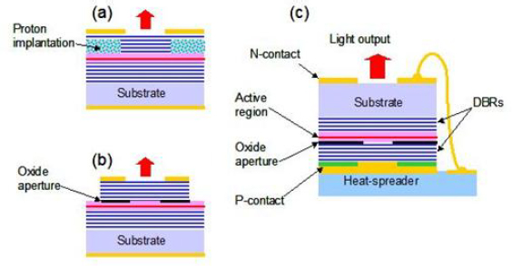
FIGURE 4-3 Several different VCSEL structures. SOURCE: Courtesy of Princeton Optronics, Inc.
and off in the 10-100 ps range, allowing direct current modulation for data rates in the tens of gigahertz. Since the fabrication process is similar to semiconductor integrated circuits (ICs), it is possible to construct many devices at one time, providing a major cost advantage over edge-emitting diode lasers. Finisar3 claims to have shipped over 150 million devices, which also find application as the source in an optical mouse. Future large-scale applications are likely in optical interconnects for high-speed electronics systems and in fiber-to-the-home.
More recently several groups have developed arrays of VCSEL devices to produce much higher total powers, although the beam quality is not high since the devices are incoherently combined. The main challenge for high-power arrays is heat removal, where the desire to have a high areal density of devices to improve brightness conflicts with the need to remove power. Princeton Optronics has demonstrated 230 W of 976-nm CW power from a 5 × 5-mm array and 925 W of QCW power from the same area.4
VCSELs had been limited in wavelength coverage to 650-1,300 nm primarily because the GaAsbased technology used to manufacture the electrically pumped devices cannot extend beyond that region. Recently, however, devices operating in the 1,500-nm region have been reported, based on the InP semiconductor, and are expected to find wide use for higher-speed fiber applications where the low dispersion of silica fibers at 1,500 nm allows 10 GHz and higher long-distance links. Development of the longer-wavelength VCSELs is intense at this writing, given their large potential in the telecom industry.
Quantum Cascade Lasers
Unlike the interband diode lasers just discussed, quantum cascade lasers (QCLs) rely on a totally artificial gain medium made possible by quantum-well structures, a process sometimes referred to as band-structure engineering. The gain from a QCL relies on transitions entirely from electronic states within the conduction band of the material, as modified by the quantum well structure. Typical devices are fabricated on InP and employ GaInAs/AlInAs quantum wells, which are formed from nanometer-thick
____________________
3 See http://www.finisar.com/sites/default/files/pdf/Finisar_infographic_timeline_web.pdf.
4 J.-F. Seurin, C.L. Ghosh, V. Khalfin, A. Miglo, G. Xu, J.D. Wynn, P. Pradhan, and L.A. D’Asaro, 2008, “High-power vertical-cavity surface-emitting arrays,” in High-Power Diode Laser Technology and Applications VI, M.S. Zediker, ed., Proc. SPIE 6876: 68760D.
layers, typically 10-15 in number. Devices based on other material combinations have been demonstrated but show inferior performance. Since the energy separation of the states is a function of the structure, it can be adjusted to generate a wide range of wavelengths, covering approximately 3.5-30 and 60-200 µm, with the latter falling in the terahertz region. The gap in long-wavelength coverage is due to the strong phonon absorption region of the semiconductor, which overcomes the gain in the quantum wells, while the short-wavelength limit is set by several factors, including fabrication difficulties with the required quantum-well alloys and losses due to scattering among different energy states in the conduction band. Different materials systems, now under development, allow operation at shorter wavelengths.
Laser operation comes through injection of a current of electrons through the quantum-well structure, resulting from a voltage applied across the structure. Both the efficiency and gain would be low if the device employed just one quantum well, since the energy of the emitted photon is small compared to the energy required to put an electron in the conduction band. This drawback is overcome by fabricating a structure consisting of multiple (typically 25-75) quantum wells in series, with another heterojunction structure, the “injector” through which the electron tunnels from one quantum well to another. Figure 4-4 is a simplified, partial schematic of a QCL structure with distance as the horizontal axis and energy as the vertical, showing the energy levels for the electron with voltage applied across the structure length that creates the gradient in energy. The QCL name comes from the “cascade” process of one electron interacting with multiple quantum wells as it crosses the structure. The one electron creates multiple photons, corresponding to the number of quantum wells in the device, thereby greatly improving the efficiency. As with edge-emitting interband lasers, the laser power is emitted perpendicular to the current flow through the layers, so that a given quantum well interacts with only a thin slice of the laser mode.
One of the remarkable features of QCLs is that they are able to operate in the mid- and long-wave IR regions without the need for cryogenic cooling, even in the CW mode. This is not possible with interband diode lasers at the same wavelengths, since the high thermal population of the conduction band turns such narrow-bandgap diodes into, essentially, short circuits at ambient temperatures.
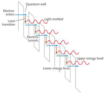
FIGURE 4-4 Simplified diagram of a quantum cascade laser. SOURCE: Courtesy of Laser Focus World.
Interband Cascade Lasers
A related semiconductor laser that has features of both interband and cascade diode lasers is the aptly named interband cascade laser (ICL). The operation of the device relies on multiple quantum-well structures, but now both electrons and holes are involved, and the quantum-well transitions are between an upper state in the conduction band and a lower state in the valence band. The material system commonly used involves either GaSb or InAs substrates, with alloys of InAs, GaSb, and AlSb employed for the quantum-well and injector structures. There are two advantages of the ICL over the QCL: (1) shorter-wavelength operation (at room temperature from 2.9 to 5.7 µm, with cryogenic operation from 2.7 to 10.4 µm), and (2) the ability to lase with much lower electrical powers (by a factor of 30 or so) than QCLs, since the transition lifetimes are much longer. As with conventional interband edge-emitting diode lasers, one would expect difficulty with long-wavelength operation at room temperature, and QCLs have an advantage there.
The current state of the art is summarized in Appendix C, Table C-2, for both QCLs and ICLs, but, as with conventional interband lasers, these numbers will change in the next 10-15 years.
Solid-State Lasers
The laser transitions for solid-state lasers occur (with a few exceptions) between energy levels of ionized atoms from the 3-D transition-metal group (Sc to Zn), from the ionized rare earth group, or from the lanthanide series of elements (La to Yb). The atoms are “hosted” in solids (crystals, glasses or ceramics) and are added as dopants to the mix of elements used to make the solids. The ions giving rise to laser operation are referred to as the active ions.
The first laser to operate was based on an artificial ruby crystal, which, in fact, consists of 3-D transition-metal Cr3+ ions hosted in Al2O3, a material known as corundum or sapphire. (“Sapphire” to the technical community is a transparent crystal, not to be confused with the naturally occurring, colored gemstone of the same name.) For transition metals, laser operation can be found from doubly to quadruply ionized atoms. The 3-D electronic states of transition metals have a reasonably large spatial extent, and thus interact strongly with the host crystal. Accordingly, the laser properties of transition-metal-doped solid-state lasers depend strongly on the host crystal.
In contrast, for the rare earths the laser transitions are primarily among different energy levels of 4f electronic states, and these, because they have a much smaller spatial extent than the 3-D states, are much more insensitive to the host crystal. With a few exceptions, a given rare earth in the same ionization state (almost exclusively triply ionized) will provide laser operation at a wavelength that is nearly independent of the host crystal.
The interaction between the host crystal and the active ion also has a profound effect on the span of frequencies/wavelengths where there is optical gain for the laser, referred to as the “linewidth.” In the case of the rare earths, and for some levels of the transition metals, when the ion changes electronic state, the surrounding atoms (the lattice) stay in the same position. Figure 4-5, left, illustrates the case when there is no lattice change, with a drawing referred to as a configuration-coordinate diagram. The horizontal axis is some measure of the lattice position (say, the separation of all the surrounding atoms from the active ion) while the vertical axis represents the combined energy of the lattice and the active ion. In the so-called harmonic approximation, the system energy increases quadratically as the coordinate moves on either side from the lowest-energy, or equilibrium position. In the classical physics view, this movement will occur as the lattice vibrates from being at some finite temperature. In a more quantum-mechanical treatment, even at absolute zero, the uncertainty principal means that there is a distribution of displacements about equilibrium. The quantum-mechanical treatment also shows that the vibrational energy is quantized, with the vibrational quantum states called “phonons.” From Figure 4-5, left, assuming that there is no displacement in the equilibrium position between the ground state and the excited state, and that the quadratic change energy with displacement is the same, then the energy
difference for light being absorbed (upward transition) and that being emitted (downward transition) is the same and independent of the displacement. One key and generally valid assumption is that the electronic transition occurs much faster than the lattice vibrates (Franck-Condon approximation) and so the lattice remains “frozen” during the transition. In the diagram, this is why upward and downward transitions are shown as vertical arrows.
In this simple picture, the spectral width of both absorption and emission would be zero, and would be at the exact same energy. In reality, other effects, especially that of phonons in disrupting the phase of the light making the transitions, lead to a finite linewidth that is a tiny fraction of the transition energy, on the order of 10-4 to 10-5 of the transition frequency/wavelength. This is several orders-of-magnitude smaller than for semiconductor diode lasers.
Figure 4-5 right, shows a configuration coordinate diagram for the case when the electronic transition causes the lattice to shift its equilibrium position. One important dynamic is that when the active ion is put into the excited state, the lattice reaches its new equilibrium position on a timescale of picoseconds. As noted, when an electronic transition takes place, it is much faster than this, but for the ions of interest, the probability of this transition actually occurring is very low on a picosecond timescale, so the lattice gets to its new position (“relaxes”) before any light is emitted by a transition back to the ground state.
Two important things result from this. First, the energies, and hence the frequencies of light absorbed in electronic transitions from the ground state to the excited state, are generally higher than for light emitted by transitions from the excited to the ground states. Second, it is evident from Figure 4-5 and the lengths of the arrows, that there can be a range of energies for either absorption or emission, due to the displacement of the two parabolas. The linewidths for absorption and emission can be very broad, on the order of 10-20 percent of the central energy.
As noted in the introductory portion of this section, unlike semiconductor diode lasers, which convert electrical power directly to laser power, solid-state lasers need a source of light to operate, which typically is driven by electrical power. The optical pumping process requires that the solid medium absorb light, which then must result in a population inversion between the upper and lower laser levels.
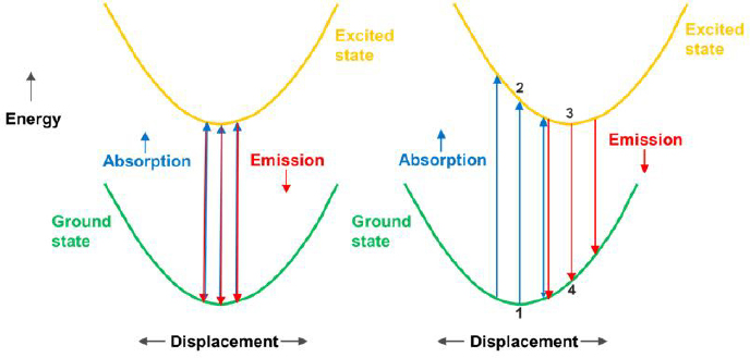
FIGURE 4-5 Left: Configuration coordinate diagram, no change in crystal. Right: Same but with a shift in crystal atomic positions.
A simple electronic system with just two energy levels and no lattice displacement (Figure 4-5 left) cannot be used to make a laser, since the material becomes transparent when a population inversion occurs. At least one higher level is needed to absorb the light, but that level must be able to transfer its excitation to the upper laser level. If the laser transition then occurs to the lowest energy level of the active ion, laser action is possible only when a substantial fraction of the ions are pumped into the upper laser level. This type of laser operation is referred to as “3-level.” If the laser operation is not to the lowest energy level but to a higher level, and that level is high enough in energy that in thermal equilibrium the population of the level is small enough to not affect laser operation, the laser operation is “4-level.” For systems where the lower level is above the ground state but has a non-negligible population, the designation is sometimes called “3½-level.”
In Figure 4-5 right, it is evident that, even with only two electronic levels, it is possible to have 4-level operation. As marked in the diagram, pump light creates a transition from the ground state in equilibrium position (1) to the first excited state in nonequilibrium (2), which then relaxes to the equilibrium position (3) and makes a laser transition to the nonequilibrium ground state (4). This type of laser operation is often called phonon-assisted or vibronic.
The ruby laser is an example of a 3-level laser, with a narrow-line (nonvibronic) laser transition (the so-called “R-line”) terminating on the ground state but with the pumping absorption lines caused by broadband vibronic transitions. These, with very high probability, deliver their excitation to the upper laser level by a so-called nonradiative process that makes up the difference in energy between the pump levels and the upper laser level by the generation of multiple phonons, often called “multiphonon relaxation.” The measured absorption coefficient for ruby shows three broad peaks at 250, 400, and 550 nm due to vibronic transitions, all of which are effective in exciting the upper level of the R-line transition at 694.3 nm.
Shortly after the ruby laser was demonstrated, laser researchers were able to operate solid-state lasers based on rare earth elements. The challenge for rare earths was in finding the right combination of energy levels among all the possible ions from that series. The most effective dopant was quickly established as neodymium (Nd3+); a partial, simplified energy-level diagram for the ion appears in Figure 4-6. The most common laser transitions for the ion occur in the 1050-1,080-nm region, from level E3 to level E2. Optical pumping is possible from the ground state (E1) to a multiplicity of levels (E4), all of which are efficient in exciting level E3 by multiphonon relaxation, with energy cascading down one level to another and finally ending up in the upper laser level. A key reason that the Nd3+ ion works well as a laser is that there is a large gap in energy from E3 to the next-lower level, so much that there is very little probability of multiphonon relaxation, and energy that winds up there can be extracted effectively by laser action. Another key to the success of Nd3+ lasers is that level E2 is sufficiently above the lowest energy level so that it has only a negligible population at normal temperatures. On the other hand, energy in that level can rapidly cascade down to the ground state, and not build up to the point that laser action stops. Thus, the Nd3+ ion provides true 4-level operation.
The right-hand side of Figure 4-6 indicates that the simplified energy levels shown as thick bars are in fact composed of multiple levels, a result of the splitting of the energy states of the rare earth ions by interactions with the surrounding atoms of the host crystal. The cluster of multiple levels indicated by the thick bars are often referred to as “manifolds.”
Given all these conditions for effective laser operation, it may not be surprising that, among the total of 13 triply ionized rare earth ions that could support laser operation, only Nd3+ has all of the characteristics just described. The other common rare earth laser ions, which include Er3+, Tm3+, Ho3+, and Yb3+, will be discussed below, but they all have one or two unfavorable characteristics that must be overcome for effective laser operation. As discussed below, a combination of laser-based optical pumping and the use of fiber formats has opened up a wide variety of uses for these ions.
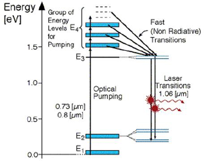
FIGURE 4-6 Simplified energy-level diagram for an Nd3+ ion.
SOURCE: Courtesy of Rani Arieli, Weizmann Institute of Science.
An alternative Cr3+-doped crystal, BeAl2O4, known as alexandrite from the gem of the same name, emerged from work in the late 1970s and presented a case where the level giving rise to the vibronic transition was, like ruby, higher in energy than the R-line level but close enough so that it was partially excited by optical pumping. Vibronic laser action is possible at room temperature around 760 nm, but the optical gain is low and the tuning range is reduced due to excited state absorption (ESA). By running the crystal well above room temperature, it is possible to improve the laser characteristics and provide tuning from about 720-860 nm. The low gain has limited applications in areas requiring generation of high-energy pulses.
The demonstration in 1982 of the Ti3+-doped sapphire (Ti:sapphire) laser provided a system with a well-known host crystal and a new laser ion. The single d electron of the Ti3+ ion provided a system similar to that diagrammed in Figure 4-5 right, with somewhat more complexity due to the details of the vibronic levels. ESA is not a factor since there are no higher-lying 3-D electronic levels and, in sapphire, other possible transitions are too high in energy. Absorption and emission intensities as a function of wavelength appear in Figure 4-7, along with the spectral distribution of the optical gain, which is red-shifted owing to the details of the Einstein relation of the measured emission spectra to the gain spectrum. The half-width of the gain spectrum is about 100 THz in frequency space, the widest of any known laser medium, and the system has been tuned from 660 to 1,100 nm.
A unique class of solid-state media has recently emerged, based on divalent transition metals doped in semiconductors, the most well-developed of which is the dopant Cr2+ in ZnSe. As with Ti:sapphire, the vibronic transitions lead to very broad linewidths, but the transitions are centered in the mid-IR region, around 2,500 nm for the case of Cr:ZnSe, which has been tuned from about 2,000-3,500 nm.
Further discussion of solid-state lasers below considers the two main formats for these systems, bulk and fiber.
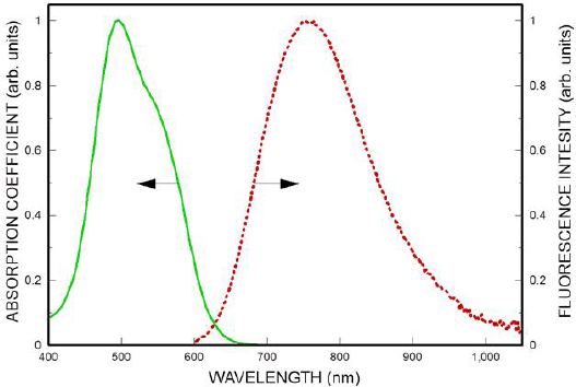
FIGURE 4-7 Absorption and emission spectra for Ti:sapphire. SOURCE: Courtesy of Peter Moulton, Q-Peak, Inc., http://www.qpeak.com/.
Bulk Format
Solid-state lasers in bulk format are based on active ions doped in crystals, glasses, or ceramics. The material can be fabricated in a variety of shapes and must allow optical pump power to be transmitted into the material, as well as allow the generated laser power to spatially overlap with the region of material that is pumped. Figure 4-8 shows a schematic of the first ruby laser, where the ruby crystal was fabricated in the form of a rod, 1 cm in diameter by 1.5 cm long and the laser cavity employed mirrors deposited directly on the polished ends of the rod. A helical xenon-gas-discharge, quartz-envelope lamp, originally developed for flash photography, surrounded the rod and was in turn surrounded by a reflecting cylinder (“pump cavity”) to help concentrate the light from the lamp onto the barrel surface of the rod. Ruby has strong visible-UV-region absorption bands, which overlap well with the emission spectrum of the lamp.
The basic arrangement in Figure 4-8 is still employed today for many lamp-pumped solid-state laser systems. The helical lamp is now usually replaced with a linear-discharge lamp, and pump cavities may be formed as a cylindrical ellipse, whose inside is coated with a highly reflecting metal like silver and with the rod and lamp each centered in one of the foci. Alternative cavities may employ a diffuse reflector to help even out the distribution of pump power in the rod. Typical rod diameters are 3-12 mm and lengths are 50-150 mm, though high-energy systems may use much larger sizes.
The simple example of the lamp-pumped laser of Figure 4-8 is used to make three key points about bulk-format solid-state lasers:
• Compared to semiconductor lasers, the spatial region over which laser action occurs is generally many orders of magnitude larger, for both the laser beam area and the volume involved in lasing. Bulk solid-state lasers can generate much higher powers from a single laser in CW operation and even more peak power simply because of the larger areas and volumes involved. For efficient laser operation, it is important that (1) a large fraction of incident pump light is absorbed in the material and (2) the spatial overlap is high between the large pumped volume and the laser beam either generated or
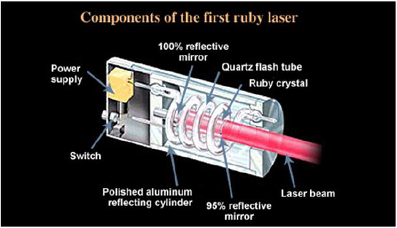
FIGURE 4-8 Schematic diagram of first ruby laser. SOURCE: Lawrence Livermore National Security, LLC and the Department of Energy.
amplified in the material. For the simple design in Figure 4-8, the latter is accomplished by making an optical cavity out of the rod itself.
• For optical pumping, at least some fraction of the absorbed pump power must be of a shorter wavelength than that of the laser, in order to create the inverted energy level population in the material. Generally, all of the energy difference between pump and laser photons is taken up via nonradiative processes that generate phonons, and the measurable effect is a rise in the laser material temperature. Unless the heat is removed, laser action will eventually stop from a variety of high-temperature effects, the most extreme being melting of the material. For the laser in Figure 4-8, heat from the rod could be removed by flowing air around the rod or, more commonly, by placing the rod inside a transparent cylinder and flowing a transparent liquid, usually water, around the outer rod surface.
• Once the laser material is actively cooled, since the material has a finite thermal conductivity, the flow of heat leads to a variation in temperature in the material. For the case of the rod in Figure 4-8, the center of the rod will be hotter than the cooled outside surface. All materials expand (or in a few cases contract) with increased temperature, and the temperature difference inside the rod leads to different levels of expansion, which in turn create stress in the material. Ultimately, at sufficiently high levels of power the material may fracture from this stress. Below the fracture limit, the optical properties of the material are changed. The stress changes the refractive index and polarization properties of the material through the stress-optic effect. More important, since the refractive index of materials changes with temperature, the gradient in temperature leads to a nonuniform refractive index. The net effect of the changes is to change the properties of the laser beam passing through the material. The changes are pump-power dependent.
Many of the engineering challenges and performance limitations of bulk solid-state lasers center on the issues described above.
Host Materials
The effect that the choice of host material has on these issues is considered first. The desirable host material properties are these:
1. Availability in a size suited for the pumping, lasing configuration; low optical loss at the pump and laser wavelengths; ability to support active-ion doping levels high enough to absorb the pump light in the desired volume.
2. High mechanical strength to avoid fracture at the desired power level, high thermal conductivity, and low thermal expansion coefficient.
3. High thermal conductivity, small change in refractive index with temperature, and small change in refractive index and polarization properties with stress.
Particularly for the rare earth dopants, several hundred different host crystals have demonstrated laser operation, but only a handful have found widespread use because they best satisfy all of the requirements listed above:
• Y3Al5O12 (YAG). A member of the very large family of garnet-structured crystals, YAG emerged from research in the 1960s as having the best combination of properties for hosting rare earth materials, including high thermal conductivity and good mechanical strength. It remains in wide use at present for a variety of industrial and medical applications and is also the basis for all laser-designator systems, as its primary operational wavelength when doped with Nd3+ ions, 1,064 nm, matches the current inventory of laser-guided munitions. A serious drawback is in the growth of single crystals, which require furnaces to operate above 1,950° C to produce a liquid from which crystals are pulled. (Reportedly, at one point the production of YAG in New Jersey represented the largest single use of electrical power in that state.) Recent advances in ceramic YAG, which is made up of randomly oriented, micrometer-sized single crystals, have allowed fabrication of much larger materials. The successful use of ceramic materials for lasers is a recent development that required significant advances in technology to essentially eliminate the scattering of light associated with the boundaries between the microcrystals making up the ceramic. The demonstration of the most powerful CW solid-state laser, 100 kW from Nd:YAG, as part of the Joint High Power Solid State Laser (JHPSSL) program at the U.S. High Energy Laser Joint Technology Office involved the use of ceramic laser material.5
• YVO4 (vanadate). One important parameter of the electronic transitions involved in pumping and laser action is the “cross section,” given in units of area. When it is multiplied by the volume concentration of laser ions, the resultant value provides a measure of the pump absorption or laser gain per unit length. Electronic transitions for solid-state lasers ions generally take place in the same electronic shell (3-d or 4-f) and are thus “parity forbidden,” which in practical terms means they would have very small, or in some cases zero, cross sections if they could somehow be suspended in free space. Once the ion is placed in a crystal, the surrounding ions create a lower symmetry than free space, mix in other electronic states to the electronic wave functions for the ion, and greatly enhance the cross section. This process is sometimes called activation of the transitions. For most of the host crystals for rare earths, the laser cross sections fall in a fairly limited range of values. The crystal YVO4 and some related compounds have unusually low-symmetry surroundings for rare earths and induce cross sections about an order of magnitude higher than other hosts. This leads to efficient absorption of pump light in short lengths of material and very high optical gains for rare earths, allowing construction of diode-laser-pumped miniaturized devices, such the common “green” laser pointer, as well as moderate-power, efficient, high-pulse rate lasers for applications in laser materials processing and high-pulse rate laser imaging systems. By a fortunate coincidence, the prime Nd: YVO4 wavelength of 1,064 nm overlaps that of Nd:YAG, making it possible to build specialized hybrid lasers for some applications.
• LiYF4 (YLF). The fluoride-based material YLF has several unique properties, including much weaker thermal distortion effects than oxide materials and natural birefringence (see below), along with favorable laser properties for some rare earth dopants. The main drawback is a reduced mechanical strength compared to most oxides.
____________________
• Al2O3 (sapphire). Sapphire has thermal and mechanical properties superior to those of all other host crystals, and when undoped it finds applications ranging from high-end watch crystals to tank windows. These properties were key to operation of the ruby laser, as many other host crystals would have fractured when pumped to the levels (several hundred Joules into the flash lamp) required by the 3-level Cr3+ transition. Unfortunately, sapphire does not accommodate rare earths at any reasonable doping level, and so after ruby it found little use in solid-state lasers until the demonstration of the Ti:sapphire broadly tunable laser. The sapphire host, besides having excellent thermo-mechanical properties, also situates the Ti3+ ion in a low-symmetry crystal environment, thereby inducing large absorption and emission cross sections. Due to this unique combination of properties, sapphire remains the only effective host for Ti3+-based, broadly tunable solid-state lasers.
• ZnSe. The material ZnSe and similar II-VI compounds have in the past found widespread use for IR-transmitting windows, with acceptable levels of mechanical strength and hardness. Chemical vapor deposition (CVD) techniques have been developed to grow large slabs of polycrystalline (i.e., ceramic) material with very low optical losses. As a host material for Cr2+ and other divalent transition metals, it provides a low-symmetry (tetragonal) environment, which leads to lower-energy transitions with large cross sections. The low phonon energy of the material minimizes nonradiative decay of the longer-wavelength transitions characteristic of divalent ions in the tetragonal environment.
• Glasses. Glass materials represent a disordered, or amorphous, arrangement of atoms. For lasers, glasses are generally based on silicate or phosphate structures, or “formers.” On a microscopic scale, active ions in glasses have slightly differing surroundings for each ion. The fine-detailed structure in the manifold levels for rare earth ions in glasses is thus smeared out (inhomogeneously broadened) when one measures their absorption and emission properties. This allows glass-based materials to have much broader absorption bands for pump light and broader continuous tuning ranges than crystal and ceramic hosts. On the other hand, the effective cross sections are lowered as well, reducing the gain and length for laser action. A big advantage for glass hosts is that they can be cast from liquid form into arbitrary and very large shapes to allow generation of very high energy pulses. The world’s most energetic laser, the Nd:glass-based, 4-megajoule-level, National Ignition Facility in Livermore, California, uses about 3,000 large plates of laser glass, each 0.46 × 0.81 m in area,6 occupying a space equivalent to three football fields. The significant disadvantage of glasses for bulk lasers is their poor thermal conductivity, a direct result of their amorphous nature. They are not capable of high-averagepower operation and find use primarily in single-shot or low-pulse-rate applications ranging from handheld rangefinders (1 pulse/s) to the NIF (1 pulse/day). (A 4-MJ pulse in 24 hours leads to an average power of around 50 W, less than that of a 1-cm-long diode laser.)
Beam Quality and Thermal Effects
One of the significant challenges in bulk solid-state laser design and engineering centers on the effects of thermal distortion of the laser material’s optical properties (“thermo-optic distortion”) on the beam quality of the laser output generated by the material. The choice of pumping devices (lamps or diode lasers) plays an important role and is discussed in detail in the next section.
For bulk solid-state lasers, modern system designs for oscillators almost always employ “external” resonators formed by dielectric-coated mirrors, sometimes including internal lenses and sometimes using a coated end of the laser material as one of the resonator mirrors. The properties of the laser output beam are set by the resonator configuration, as modified by any thermo-optic effects in the laser material.
For materials shaped like simple cylindrical rods and cooled through the cylindrical surface, the temperature distribution can be approximated by a parabolic profile (transverse to the beam), peaking in the center of the rod. The corresponding optical effect is to make a rod behave, to a first level of
____________________
6 See https://lasers.llnl.gov/about/nif/how_nif_works/amplifiers.php.
approximation, as a lens. The lens is positive for the majority of materials, which exhibit a positive change in the refractive index with temperature. Additional optical distortions come about from the stress-optic effect, which converts the stress in the material from the thermal gradient into a change in refractive index. In rod configurations the stress-optic effect can also be approximated as creating a simple lens. For many materials, the two effects are additive, but in a few, particularly fluoride-based materials, the change of refractive index with temperature is negative, while the stress term is positive, leading to a reduced level of “lensing.” Smaller levels of optical distortion result from changes in the shape of the laser material due to nonuniform thermal expansion of the material as a result of the temperature gradient.
Another stress optic-effect is a distortion of the polarization of light passing through the material due to “stress-induced birefringence,” which in rods leads to a polarization state that changes over the cross section of beam. For crystals that are naturally birefringent, such as vanadate and sapphire, the natural birefringence typically dominates stress birefringence, and one can avoid any change in, say, a linearly polarized beam by aligning the polarization with one of the crystal axes. Isotropic materials such as YAG and all glasses are, however, susceptible to stress-induced birefringence, and this is an issue since linearly polarized light is required to drive many of the nonlinear processes discussed below.
In theory, it should be possible with any bulk solid-state laser to effectively generate a large fraction of power from a single, diffraction-limited, transverse mode of the resonator, since the diameter of the single mode can be made arbitrarily large by the choice of cavity design. In practice, for the laser wavelengths and resonator lengths used for bulk solid-state lasers, operating with “stable” cavities that produce more than several millimeters of beam diameters is impractical, since either the required angular alignment of the mirrors becomes unreasonably exacting or the thermo-optic effects in the laser material make the beam properties highly dependent on the exact pump power of the system. For high-gain lasers, such as Nd:YAG-based devices running in a pulse-pumped mode, it is possible to employ so-called “unstable” resonators that can provide single-mode 5-10-mm diameters, but these have to date been employed only in laboratory-based lasers.
To get around the limits of cavities, one can design a relatively low-power laser oscillator optimized for single-transverse-mode operation, and then amplify the oscillator in one or several amplifier stages, where the laser mode is expanded by telescopes to fill the size of the pumped region in the amplifier. This is the standard approach for most high-power systems and is termed a master oscillator power amplifier (MOPA) system.
Ultimately, thermo-optic effects in the laser material will limit the beam quality of the system by adding phase distortions across the area of the laser beam. While simple external lenses can correct the first-order effects in rod-geometry designs, as the thermal gradients increase with pump power, the higher-order levels of distortion become significant. In recent high-power laser systems design, so-called adaptive optics, first developed to correct for the linear phase aberration effects of atmospheric turbulence on laser beams, can be applied to correcting the more complex distortions in materials running at high powers, typically through the use of feedback loops that seek to maximize beam quality.
There are several material geometries beyond simple rods that attempt to reduce thermo-optic effects. Notably, if the heat flow is along the direction of the optical beam, the thermal gradient is as well. When the material is uniformly pumped, all sections of the beam experience the same refractive-index change and thus the beam phase-front is undistorted. Typical designs employ thin plates, often in the shape of a disk, where the large surface can be cooled by high-velocity liquids or by contact with a transparent, high-thermal conductivity crystal. Power limits are from stress, as always, and this is minimized by the use of thin crystals. However, if the crystal becomes too thin, it will not absorb, in a single pass of light through the material, a sufficient fraction of the incident pump power.
A recent design, the so-called thin-disk geometry, has been made possible through the development of diode pump lasers (discussed below.) Here a thin disk of material (on the order of 0.1-mm thick) is cooled by contact of one of the large faces to a metal heat sink, with the contacted face employing a dielectric coating that is designed to be highly reflective at both pump and laser wavelengths. The design employs optics that arrange for the pump light to make many passes back and forth through the laser material, effectively increasing the optical path for the pump light and facilitating efficient
absorption. (This arrangement would not be possible with lamp pumping.) Ultimate limits to beam quality are set by the inevitable deviation of heat flow from the desired direction along the thin axis of the material and the resultant stresses. For thin-disk lasers the mechanical distortion of the material cannot be ignored as a thermo-optic effect, and there is a limit to how large an area of the crystal can be used while still maintaining a high beam quality. One disadvantage of the thin-disk design is the relatively low gain of the system because of the short length of active material, and typical designs are with oscillators only, with low-loss laser cavities.
Another geometry used for high-power, high-beam quality systems is the zig-zag slab design. In this case the material is fabricated as a thin slab, but with a rectangular geometry. The laser beam is arranged to reflect back and forth in the thin direction (hence the descriptor zig-zag), off polished faces of the slab. This has the advantage that all parts of the optical beam experience the same thermo-optic distortion in the zig-zag direction. Distortion in the other direction is minimized by designing the pump beam to be as uniform as possible. Lamp pumping is typically done through both large faces of the slab, with cooling of the same faces by a flowing liquid. Diode pumping can be done through one face, with the other face cooled by contact with a metal heat sink. Another configuration, with the diode pump light directed along the long length of the slab, is discussed in the next section. This is the configuration used in the most powerful bulk solid-state laser (as of this writing).
Many common solid-state lasers, such as those used for materials processing, laser target designation, range-finding, and imaging at relatively short distances do not require diffraction-limited output, and resonator designs for such systems emphasize some combination of efficiency and high stability against vibration or system temperature change.
The actual relation between power output and beam quality is set not only by the laser material and resonator design but also by the pumping source.
Pumping Systems
Incoherent, lamp-based pump sources were the standard for bulk solid-state lasers until the 1980s, when development of high-power diode lasers brought about a major revolution in high-performance systems.
Lamps are still widely used for systems where cost or simplicity is important. For lamps operating in the pulsed mode (“flashlamps”), the typical design uses approximately atmospheric-pressure xenon gas, typically contained in a fused silica tube with tungsten-based electrodes on both ends and driven by a high-current electrical discharge. Lamp diameters are from 3 to 19 mm, and lengths can range from 2 cm to 1 m, depending on the system and energy required. Well-designed xenon lamps are 50-60 percent efficient in converting electricity to light, which they produce in a spectrum that resembles a hightemperature (6000-10000 K) blackbody with discrete emission lines in the 820-1,000-nm region. As the lamp discharge current increases, the line spectrum becomes a smaller fraction of the total spectrum. The energy limit for a flashlamp is set by its “explosion energy,” which is proportional to the inner area of the containing tube, and if the lamps are run at less than 30 percent of their explosion energy typical shot lifetimes before lamp failure are 107 to 108, with NASA claiming to have shown a 109-shot lifetime in one system.7
For CW lasers, one employs arc lamps, which differ in some details from flashlamps in the electrode and tube designs, as well as use of a multi-atmosphere fill pressure. For the most widely used laser application for pumping Nd:YAG lasers, arc lamps employ krypton rather than xenon gas, since the narrow-line krypton spectrum is a better match to the absorption spectrum of that material. Arc lamp lifetimes range from 200 to 2,000 h, depending on the operating cycle of the laser, with the longest lifetime seen for lamps running 24/7.
____________________
7 L.J. Richter, F. Schuda, and J.J. Degnan, 1990, “Billion-shot flash lamp for spaceborne lasers,” Proc. SPIE 1223: 142, Solid State Lasers, doi:10.1117/12.18406.
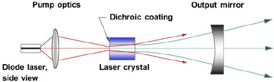
FIGURE 4-9 Schematic of diode end-pumped solid-state laser.
Lamp-pumped Nd:YAG lasers convert 2-3 percent of the lamp energy into laser output, with much of the lamp output not absorbed by the laser material. For flash lamps, as the pulse energy increases more of the pump power is delivered into higher levels, increasing the heat dissipated in the crystal. Despite these difficulties, lamps remain in widespread use, especially in pulsed lasers, for reasons to be discussed below.
The use of diode lasers as optical pumps for solid-state lasers was demonstrated in the 1960s, but the limited power and performance of early diode lasers kept them from widespread adoption. With improvements in semiconductor materials and processing technology in the 1980s, commercial high power single-emitter diodes with outputs of 0.2 W became available, with operating wavelengths around 808 nm, suited for pumping Nd:YAG lasers. The first important design scheme for diodes was the socalled longitudinal (or end-) pumping configuration, shown schematically in Figure 4-9. The singleemitter diode laser output is collected and focused into an approximately round beam at the surface of the laser crystal through appropriate optical design. The pump beam diameter, and the diameter of the fundamental laser-cavity mode formed by one coated mirror on the crystal and one curved external mirror, are designed to be about the same, which results in the solid-state laser output being single-transverse mode. Typical laser crystal lengths are from 1 to 10 mm.
Several major advantages of diode over lamp pumping are evident with the end-pumping design of Figure 4-9:
• Essentially all of the diode output, rather than the small fraction typical with lamps, can be absorbed by the laser material. Thus, even though lamps and diode lasers are roughly comparable in overall conversion of electricity to light, the diode output to laser output (optical-to-optical) efficiency is more than ten times greater than that of lamps.
• With the proper choice of wavelength, the amount of heating in the material from laser action for a given power is smaller with diode pumping and reaches a minimum when the pump wavelength directly excites the upper laser level in a normally 4-level laser. This leads, in turn, to less thermo-optical distortion of the laser beam by the laser material.
• As noted above, the correct choice of pump-beam and laser-cavity beam area produces a diffraction-limited output, an important characteristic. Diode lasers are limited in their ability to produce large diffraction-limited powers, but they can make high multimode powers. The diode-pumped solidstate laser acts as a “brightness converter” for high-power diode lasers, and even with the inevitable loss in absolute power from the diode pumps, the brightness of the solid-state laser is between one and two orders of magnitude brighter.
• Heat generated in the laser material can be extracted by bringing the outer surface of the laser material into contact with a high-thermal conductivity material, eliminating the need for flowing a coolant over the material. Combined with the generally more stable pump power from a diode laser, this can lead to very stable operation of the solid-state laser, important for, say, generation of a stable laser wavelength/frequency.
• Diodes can be powered by low-voltage power supplies or batteries, in contrast to the high-voltages needed to drive lamps.
• With improvements in diode fabrication, laser operating times before pump replacement are typically three orders of magnitude longer than with lamps.
Disadvantages of the diode pumps compared to lamps include the following:
• The much higher cost of diodes.
• The need to maintain the diode operating temperature within a fairly narrow range, since the wavelength of diodes does shift with temperature. For typical diode lasers in the 800-1,000-nm range, the tuning rate is about 0.3 nm/°C. For Nd:YAG pumping at 808 nm, where the absorption linewidth is about 2 nm, one must hold the diode temperature well within a 10° C range for a simple end-pumped design. More complex designs can work over much wider ranges by using several diodes, each of which works for a certain temperature range, optical designs that provide multiple passes of the pump light, and/or diodes that have built-in wavelength-stabilization optics.
Initially, with the first single-emitter diodes, the power available for pumping was well below 1 W. Today, the available power from a single device with a 100-µm-widestrip is on the order of 10 W. For higher powers there are a number of techniques that make it possible to combine the outputs of multiple single-emitters into one pump beam. Figure 4-10 shows a simple approach that converts the multiple outputs of a diode bar laser into a single fiber, whose output can then be used for end-pumping. Because the simple design does not take advantage of the fact that diode outputs are single-mode in one transverse direction, it produces a low-brightness pump beam. More sophisticated bar-based pump sources use complex imaging systems to “stack” the diffraction-limited beam components of multiple emitter outputs in a way that greatly improves brightness, leading to fiber-coupled devices that can provide CW power levels of 200-300 W from a fiber with a 200 µm diameter and a 0.22 numerical aperture fiber.
At some power level, the simple end-pumped solid-state laser design of Figure 4-9 becomes impractical. Even with improvements in diode brightness, the pump beam in the crystal diverges rapidly enough such that, for good overlap of pump and laser beams, the length over which pump power is absorbed must be kept to 1 cm or less. Power limits are due either to crystal fracture from the large thermal load in a small volume or a large amount of thermal distortion.
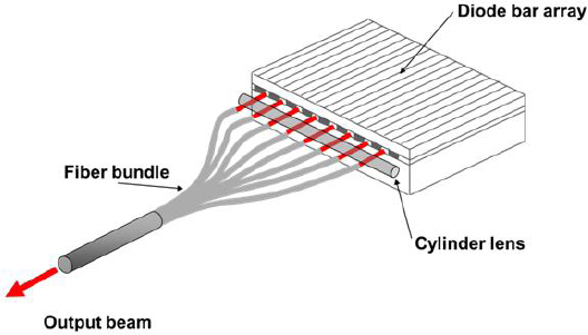
FIGURE 4-10 Optical schematic showing coupling of bar output to a single fiber.
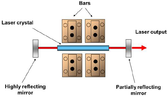
FIGURE 4-11 Schematic of diode side-pumped laser.
So-called side- or transverse-pumped designs with diodes can be employed to generate higher powers (and energies in the pulsed mode, see below), as shown schematically in Figure 4-11. Similar to lamp-pumped lasers, the pump light direction is roughly perpendicular to the laser direction, requiring the laser material to be fabricated appropriately. Cylindrical rods, thin, zig-zag slabs and other geometries can be employed, with cooling by either flowing liquid or bringing a portion of the material into contact with a metal heat sink. Obtaining good overlap with the lowest-order mode of the laser cavity is much more of a challenge than with end-pumped designs, and optical-optical efficiencies in general are lower. On the other hand, it is possible to couple much higher powers from the diode pump lasers, as many pumps can be used with one laser medium.
For side-pumping designs, diode bars are more effective in transporting light to the laser materials when they are closely stacked together, and extracting heat becomes a thermal engineering challenge. For pulsed systems with low average powers but high peak powers many more bars per square area can be put together than for CW systems. There are designs for low-average-power systems, as well as water-cooled bars designed for CW lasers such as that shown in Figure 4-12.
An example of the current state of the art of diode-pumped bulk lasers is the “gain module” design employed by Northrop Grumman in the 100-kW, CW laser built as part of the U.S. High-Energy-Laser Joint Technology Office, JHPSSL program. The module design has been commercialized by Northrop Grumman as part of the Vesta series of lasers.8
A Northrop-Grumman array employs two 36-bar vertical stacks with spacing between bars of 1.8 mm. Each bar has a cylinder lens attached to collimate the fast axis of the bar and, after that, a narrowwavelength reflecting element (a volume Bragg grating) designed to form an external resonator and control the diode wavelength. For the device design used for the JHPSSL, the operating wavelength is set to center at 885 nm and efficiently pump the upper laser level of Nd:YAG, minimizing the heat generated
____________________
8 See http://www.irconnect.com/noc/press/pages/news_releases.html?d=107455.
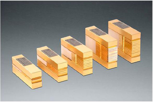
FIGURE 4-12 High-brightness, high-power stacked bars. SOURCE: Courtesy of DILAS.
in the solid-state laser material. The output of the two stacks is combined with an interleaving mirror to increase the intensity of the pump beam. Micro-channel water coolers, which provide high heat extraction per unit area, remove heat from the arrays and allow each 36-bar stack to generate a total CW power of 2.5 kW.9
Figure 4-13 (left panel) shows a schematic of the pumping and laser-material configuration for an earlier version of the gain module, based on the material Yb: YAG.10 The solid-state laser material is configured as a thin zig-zag slab, with a pumping source on each end of the slab, and pump light entering through one of the slab faces, coated to act as a reflector for the pump power. As with longitudinal pumping, the pump and laser light propagate in the same general direction, with both reflecting off the large slab faces. A majority of the slab surface area is cooled by conduction to water-cooled metal heatsinks. The figure shows lens ducts used to collect the light from the pump arrays, while the newer, Nd:YAG-based JHPSSL uses simple lenses to properly format the pump light, as is evident in Figure 4-13 (right panel), a photograph of the Vesta gain module. Four gain modules for the basis for the lowestpower Vesta laser system, and generate 15-kW of CW power in a near-diffraction-limited beam. The JHPSSL system coherently combined the outputs of seven 15-kW modules to generate the record 100 kW of power.
Alternative Rare Earths
Diode pumping has also brought back into common use several rare earth dopants, all of which had been demonstrated in the early years of solid-state lasers, but subsequently abandoned in favor of Nd3+ -doped lasers for lamp-pumped lasers. These include:
____________________
9 See http://www.northropgrumman.com/BusinessVentures/CEO/Documents/TechNote17_wavelength_stabiliz.pdf.
10 G.D. Goodno, S.Palese, J. Harkenrider, and H. Injeyan, 2001, “Yb: YAG power oscillator with high brightness and linear polarization,” Opt. Lett. 26: 1672.
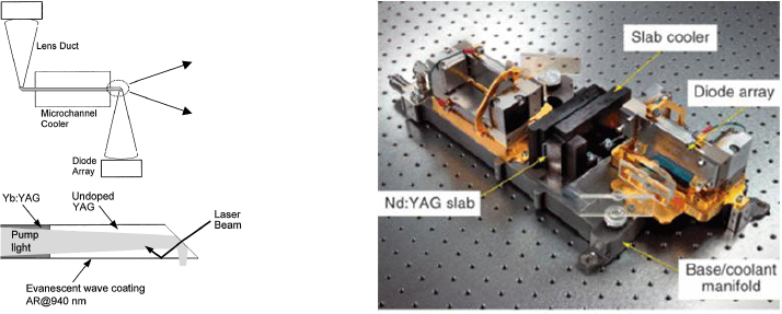
FIGURE 4-13 Left: Diagram of end-pumped slab design used for Vesta gain module. Right: Photograph of the gain module. SOURCE: G.D. Goodno, S. Palese, J. Harkenrider, and H. Injeyan, 2001, “Yb: YAG power oscillator with high brightness and linear polarization,” Opt. Lett. 26: 1672 (left) and Courtesy of Northrop Grumman Corporation (right).
• Yb3+. The Yb3+ has only a single 4-f electron and as a result has a very simple 4-fenergy-level structure, a ground manifold, and one excited-state manifold. There is enough energy separation among the levels within the ground manifold to facilitate 3½-level laser operation. For lamp pumping, the lack of excited levels leads to low efficiency in absorbing broadband pump power, but with diodes tuned to the ground-state-to-excited-state absorption band, efficient laser operation is possible. In Yb: YAG, the typical laser wavelength is 1,030 nm, while a common pump band is centered at 941 nm. The difference in pump and laser wavelength is much smaller than for typical Nd:YAG pump/laser wavelengths of 808/1,064 nm, leading to a thermal load in Yb: YAG that is about 38 percent that of Nd:YAG and 53 percent for the less common 885/1,064 combination. There are some drawbacks to Yb: YAG compared to Nd:YAG, including a much higher threshold for operation at room temperature due to the partial thermal occupation of the lower laser level, as well as a smaller gain cross section. If Yb: YAG crystals are cooled to cryogenic temperatures, laser operation becomes truly 4-level, the gain becomes comparable to Nd:YAG since the spectral linewidth decreases, and the thermal conductivity rises by an order of magnitude. Moreover, recent demonstrations of cryogenically cooled systems suggest they could find use as very high power, pulsed sources for a variety of applications. Other host crystals for Yb exhibit large gain linewidths, and these have been exploited to build diode-pumped, 100-femtosecond-pulse, high-energy sources. The Yb ionic size is very close to the Y-ion size in YAG and other Y-based materials and can be doped to levels as high as a 100 percent replacement of the Y ions. This is used to advantage in Yb: YAG thin-disk lasers, where typical doping levels can be on the order of 10 percent to raise the amount of absorbed single-pass power.
• Er3+. The ground-to-first-excited-state transition of the Er3+ ion provides laser operation in the 1,530 to 1650-nm wavelength region, desirable for active sensors since it falls in the eye-safe wavelength range. These laser transitions are 3½-level, leading to the need for high populations of the upper level to reach threshold. In addition, the energy-level structure of the ion promotes upconversion processes, where two nearby ions in the upper laser level interact, with one ion dropping to the ground state and the other ion moving to a higher energy state. This process competes with optical pumping and makes it difficult to obtain efficient operation. The best way to minimize this process is to reduce the Er doping level, but that also reduces the absorption strength and makes pumping less efficient. This
problem is worsened by the relatively small cross sections for the Er transitions, for both absorption and emission. One solution to the problem is to add Yb3+ ions into the crystal. Energy put into the Yb energy levels can transfer over to Er ions, since the two rare earths have excited states that are coincident in energy, a process called sensitization. Materials can be doped with high levels of Yb ions to provide good pump absorption and low-enough levels of Er to minimize upconversion. (For lamp pumping, Cr3+ ions can also be added, and they in turn transfer energy to Yb ions.) Unfortunately, to date, the only host materials where the sensitization process is effective are phosphate-based glasses. With diode pumping, the average-power capabilities and efficiencies of glass-based Er lasers have been increased but are still limited.11 Yb and Er glasses have found use in low-pulse-rate range finders, particularly handheld, shortrange devices. In the fiber-laser section, hybrid systems that use fiber lasers to pump bulk lasers are discussed, and Er:YAG is one bulk material that has been employed in hybrid designs.
• Tm3+ and Ho3+. As with Er-doped lasers in the 1,550-nm region, the common laser transitions for Tm- and Ho-doped materials in the 1,900-2,100-nm wavelength region, also eye-safe, terminate on the ground manifold and are thus 3½-level systems. Of the two ions, the Ho laser-transition cross sections are generally higher (by a factor of 5 in YAG, for example), but Ho has limited and weak absorption transitions for either lamp pumping or diode pumping. A common scheme for pumping employs Tm sensitization of the Ho laser, with Cr3+ sensitization added for lamp pumps. Pumping of Tm in the region around 795 nm has the special property that, with a high enough Tm doping level, there is a cross relaxation between pairs of nearby ion that generates two ions in the upper level per absorbed pump photon. Recent developments in diode-laser materials show promise for the emergence of efficient, high-power pump lasers that can drive the upper laser levels of Tm or Ho. The ions are of interest for application in a variety of eye-safe active sensors, including coherent-detection wind-sensing systems. Ho-doped bulk materials also feature in hybrid bulk-fiber solid-state lasers, discussed below.
• Pr3+. All of the ions discussed so far generate wavelengths in the infrared. Pr-doped materials have laser transitions at green and red wavelengths, as well as some near-IR transitions. The ion has narrow and weak pumping transitions at blue and shorter wavelengths and suffers from cross-relaxation processes that reduce laser efficiency at high doping levels and thus can barely operate with lamp pumping. The emergence of GaN-based blue diode lasers has made it possible to construct diode-pumped systems, and as GaN technology improves, Pr-doped lasers may emerge as a new source of direct laser operation in the visible wavelength range, with possible applications in underwater sensing.
Energy Storage and Q-Switching
Pumping power, either electrical for diodes or optical for solid-state lasers, leads to excitation of the upper laser level. If there is no laser operation, and the pump power is turned off, energy remains stored in the laser material, which decays away by spontaneous emission of photons and, in some materials, also by generation of phonons through nonradiative relaxation. In most cases, the decay is exponential, characterized by a single number, the upper-state lifetime or “storage” time. For a given pump power, the stored energy is directly proportional to the decay time, provided that only a small fraction of the ions in the material have been excited. With laser action, the stimulated emission process that gives rise to optical gain acts to extract the stored energy. The rate of extraction (or inversely, the stimulated lifetime) depends on the power in the laser beam but is of the same order as that of the spontaneous emission.
For semiconductor lasers, storage times are in the nanosecond range at best and lower in quantum-cascade devices. Transitions in solid-state lasers have storage times between 0.1 and 15 ms, with the notable exception of the 3.2-µs lifetime of Ti:sapphire. Thus, per watt of pump power, stored energies are in the nanojoule range for diode lasers and the millijoule range for solid-state lasers.
____________________
11 T. Yanagisawa, K. Asaka, K. Hamazu, and Y. Hirano, 2001, “11-mJ, 15-Hz single-frequency diode-pumped Q switched Er, Yb:phosphate glass laser,” Opt. Lett. 26: 1262.
The ability to store large amounts of energy in the laser medium is one of the key advantages of bulk solid-state lasers and is unique to them. (As noted below, fiber-format lasers, although capable of high CW power levels, have major challenges in storing energy.) The process of Q-switching allows bulk materials used as laser oscillators to deliver the stored energy in very short pulses, thereby generating high peak powers useful for many applications, including, notably, active sensing.
Consider if the pump power to a laser is turned on but a shutter is put in the optical cavity to prevent laser action. The laser material will then, after several decay times, reach a steady amount of stored energy. Also assume that the pump power is well over the threshold for laser operation. If the shutter is rapidly opened, the power output of the laser will start to build up from the thermal noise background, as the laser power circulates back and forth between the mirrors. For typical solid-state laser optical cavity lengths and levels of laser gain, this buildup takes place on a timescale of tens of nanoseconds. Eventually the power in the cavity is sufficient to start to extract the stored energy by stimulated emission and the population of the upper laser level falls. Once the stored energy returns to the threshold level, power in the cavity stops increasing and the output of the laser falls, on a timescale commensurate with the time it takes for light to decay in the laser cavity without any optical gain from the laser medium, a quantity called the “cavity lifetime.”
With the advent of diode-laser pumping, some new types of Q-switched lasers could be developed. So-called microchip lasers, made from millimeter-thick, longitudinally pumped active media such as Nd:YAG bonded directly to solid media that have saturable absorption at the laser wavelength, can generate pulses that last much less than 1 ns; this is useful for active sensing requiring high range precision.
This transient condition results in the generation of a pulse containing a large fraction of the energy initially stored in the laser material, with a width that is related to the round-trip time of light in the laser cavity. A key element in the process is the shutter, which, to avoid any loss of energy in the pulse, must change from a high-loss to a low-loss state in less time than the time required by the pulse to build up from the noise background. The shutter, for reasons dating back to the microwave origins of lasers, is called a “Q-switch” and the generation of pulses is corresponding called Q-switching.
For flash lamp-pumped or pulsed-diode-pumped lasers the optimum time at which the Q-switch goes to a low-loss state, or “opens,” is at the point in the pumping process when the stored energy is greatest. To avoid losing energy to decay processes in the upper level, optimal pulse durations should be shorter than the storage time. For flash lamps, if the lamp energy is kept constant and the pulse is made too short, the risk of lamp explosion increases; in general, however, the same lamp running at a 10 J can produce a pulse lasting from 10 µs to 10 ms, thus operating over a range of powers from 1 kW to 1 MW. For diodes, which cannot be Q-switched and generally are limited to the nearly the same power independent of pulsewidth, the pulse energy decreases with pulsewidth, so that the optimum choice of pulsewidth is slightly shorter than the decay time.
CW-pumped, repetitively Q-switched bulk solid-state lasers running at 1-100 kHz and primarily based on Nd:YAG have found wide use in micromachining a variety of materials used by the electronics industry, where the short pulses facilitate precise drilling, forming, and marking. With diode-pumping, the performance of the devices has improved in terms of beam quality and power. End-pumped designs such as that shown in Figure 4-9, short optical cavities, and high-gain laser materials such as Nd:vanadate combine to enable the generation of pulsewidths at the 1-ns level at tens of kilohertz, opening up applications for 3-D imaging sensors with high data collection rates.
One related mode of laser operation is “gain-switching,” whereby the pump power is in the form of a pulse whose duration is preferably shorter than or at least comparable to the laser buildup time. In this case the energy stored in the laser material can reach a high level before laser operation begins, and the result is generation of a short pulse similar to that of a Q-switched laser. Diode lasers can be gain-switched.
Clearly, with diodes, materials having long decay times lead to higher stored energies for the same pump power. The laser engineering trade-off is that there is an inverse relation between the gain cross section and the storage time, for desirable laser systems where the storage time is not reduced by
nonradiative processes. In addition, for the same lifetime, the gain cross section is inversely proportional to the spectral linewidth of the gain. Thus, materials system with long storage times may suffer from small cross sections, as do systems with large linewidths. One potential problem with low cross sections is that the energy per square centimeter, or fluence, in the laser pulse passing through the material has to be sufficiently high to efficiently extract the stored energy. A measure of the required level is the “saturation fluence,” which is simply the energy of a laser photon divided by the cross section. If the fluence is too high the laser system optics, including the laser material itself, may suffer optical damage and cease to function. The damage level for optics in terms of fluence is a complex and often not-wellcharacterized function of the optical material, the surface (bare or dielectric coated), pulsewidth, beam area, pulse rate, and laser wavelength, with dielectric coatings often exhibiting the lowest threshold. Threshold fluences for damage can fall in the 1-100 J/cm2 range for 10-ns pulses, with coated surfaces typically failing in the region 5-20 J/cm2.
In the other direction, if a material has too high a cross section it may not be able to store the desired energy. At high levels of stored energy the optical gain may be so high that, for oscillators, the loss on the Q-switch (hold-off) may be insufficient. Even for infinite hold-off, the laser material may start to oscillate from optical cavities formed by unwanted reflections in the material. Ultimately, stored energy may be reduced by amplified spontaneous emission (ASE), where the light emitted by the normal decay process stimulates transitions from other excited ions, thus speeding up the loss of stored energy. With oscillator-amplifier chains, the gain through the entire system may get so large that the stored energy is limited by ASE.
Thus, there are a series of trade-offs regarding the choice of materials and system designs for pulsed systems working with Q-switched pulses. Even when the source of the pulses is not a Q-switched solid-state laser but some other device—say, a pulsed semiconductor laser or, as is discussed more below, picosecond and femtosecond pulses—similar issues arise.
Table C-3 lists the characteristics of several common bulk laser materials that impact design of short-pulse systems. There is a relation between cross section and lifetime that depends on the center wavelength of the laser, with the product of the cross section and lifetime following the 4th power of wavelength, thus favoring longer wavelengths to get long storage times for the same cross section.
In terms of lasers for use around 1000-nm wavelengths, the Nd-doped crystals (except for vanadate) provide a reasonable balance of good storage time and low saturation fluences but tend to be limited in storage by ASE issues. As noted above, the vanadate material, although not well suited for high-energy storage, provides a unique capability: it generates short pulses at high rates because of its large gain cross section. The smaller gain of Nd:glass allows significantly higher levels of storage before ASE limits set in, but glass hosts are not suited for high-average-power systems. (There is a continuing interest in finding new Nd host crystals that have glasslike storage capability but high thermal conductivity, but to date no material has proven useful.) Yb: YAG at cryogenic temperatures has a Nd-like saturation fluence combined with very low thermo-optic distortion, but the cooling requirements are a challenge for many applications. At room temperature the much higher fluence levels of optics with Yb: YAG is an issue for short-pulse systems.
For the longer eye-safe wavelengths, high saturation fluences are one of the reasons that Er-doped materials are not well-suited for high-energy, short-pulse lasers, while Ho-doped materials have proven capable of moderately high pulse energies with nanosecond-duration devices. The 15-ms lifetime of Ho: YLF promoted substantial energy storage with CW-laser pumping.
Ti:sapphire stands out from the other materials because of its very large linewidth, and it has an acceptably low saturation fluence. However, its storage time requires pump pulses to be microseconds or less for efficient operation. The most common pump for high-energy Ti:sapphire lasers is a Q-switched, frequency doubled, Nd-doped laser, and the Ti:sapphire laser typically generates a gain-switched pulse as a result of the short pump pulse. Cr:ZnSe, referred to as the “Ti:sapphire of the mid-infrared,” also has a large linewidth and a short storage time and is emerging also as potential source of high-energy pulses around 2000 nm wavelength when pumped by Q-switched lasers. While the bandwidth for Cr:ZnSe in
terms of wavelength is larger than for Ti:sapphire, in terms of frequency it is less, and the latter actually determines the shortest pulsewidth for mode-locked operation, as discussed below.
Many moderate-energy solid-state lasers (for example, those based on Nd:YAG) still use flash lamps rather than diodes. If the goal is to generate a 100-mJ-energy Q-switched pulse, one would typically run the pump for 0.15 ms (compared to the storage time of 0.24 ms). Accordingly, with diode pumping, if there is 25 percent conversion of pump power, an array of diodes producing 400 mJ for 0.15 ms would be needed. This corresponds to about 2.7 kW of power. At an estimated current pricing of $3/W for a pulsed diode array, this leads to a cost of $8,000 just for the pump devices. The single lamp required to produce the same 100 mJ of laser energy costs about $100. Even with this cost difference, systems for man-portable applications may use diodes, since the higher efficiency and simpler cooling leads to a significant reduction in weight. For airborne systems, the longer lifetime of diode pumps may justify their use, given the high costs of removing a laser from the system to do a pump replacement. Mode-Locking and Chirped Pulse Amplification
Even when a solid-state laser generates a single spatial, or transverse mode, it can generate a large number of longitudinal modes. The resonant frequencies of the longitudinal modes of an optical cavity correspond to a large integer times the speed of light divided by the round-trip optical path length of the cavity. For a 50-cm-long cavity, the frequencies are spaced by about 0.3 GHz. For Nd:YAG, the linewidth of the laser gain is about 180 GHz, so, in principal, that laser could oscillate on hundreds of longitudinal modes. In reality the modes compete for power in the laser medium, and in principle, if the laser is allowed to reach a true steady state, only one mode would remain operational. More typically, the modes occupy slightly different spatial regions in the material, and Nd:YAG lasers may have multiple modes that span a 10-GHz range. Remarkably, this is true even for materials like Ti:sapphire that have a linewidth 500 times larger, because of the competition among modes for gain.
The modes typically operate with random phase relationships that fluctuate with slight changes in operating conditions. If one places a time-dependent loss element in the laser cavity at exactly the frequency of the mode spacing, the lowest-loss condition for the laser leads to the modes acquiring, after some time, a fixed phase relationship among the different frequencies. If this is translated from the frequency to the time domain, this phasing leads to the generation of a steady train of pulses at a rate inverse to the mode spacing. Such phasing leads to pulses that time themselves to pass through the loss element at its minimum loss point. This general process is called “mode-locking.” The more modes that are locked together, the shorter the pulse, and how quickly the loss element changes from a high to a low state influences the number of modes. The major influence on the pulse duration is from the gain linewidth of the laser, and that puts an upper limit on the number of modes that can be locked, or, equivalently, a lower limit on the pulse duration. The product of the minimum pulse duration in seconds and the gain linewidth in Hz is a constant, depending on the exact temporal shape of the pulse, and falls in the range 0.3-0.4. For Nd:YAG, the minimum pulsewidth is about 2 picoseconds ps while for Ti:sapphire the value is 3.5 femtoseconds fs, and for Cr:ZnSe about twice that. Pulses that have the minimum value or duration for a given spectral linewidth are called “time-bandwidth limited.”
Typical mode-locking schemes could employ an electro-optic or acousto-optic loss modulator, but they have sinusoidal variations in loss and generally are not able to generate pulses that fully occupy the available linewidth of the laser. Passive loss elements based on semiconductors (or recently, graphene) that show a rapid reduction in loss with intensity can produce much shorter pulses. A breakthrough in mode-locking of the large-bandwidth Ti:sapphire laser occurred with the accidental discovery that the laser medium itself could provide a fast-switching loss element based on the nonlinear refractive index of sapphire. This led to generation of 100-fs pulses, and subsequent refinement of this
FIGURE 4-14 Interferometric autocorrelation signal from mode-locked Ti:sapphire laser showing data and fit to 6.5 ns pulse. SOURCE: I.D. Jung, F.X. Kärtner, N. Matuschek, D.H. Sutter, F. Morier-Genoud, G. Zhang, U. Keller, V. Scheuer, M. Tilsch, and T. Tschudi, 1997, “Self-starting 6.5-fs pulses from a Ti:sapphire laser,” Opt. Lett. 22: 1009.
technique, combined with advances in the optical resonator mirrors, has led to Ti:sapphire lasers that can generate pulses approaching the 4 fs limit. The pulses contain only a few optical cycles, as is evident from the data in Figure 4-14, for a pulse with an estimated pulsewidth of 6.5 fs.12
Typical mode-locked oscillators operate at a pulse rate of around 100 MHz, with an average power of 1-10 W, leading to per-pulse energies of 10-100 nJ. For a Ti:sapphire laser producing 10-fs pulses, each pulse has a peak power of 1-10 MW, comparable to the peak power of high-energy Q-switched solid-state lasers. If one sends this pulse into a Ti:sapphire amplifier system, amplification to the relatively modest energy of 1 mJ leads to a peak power of 100 GW. At typical beam sizes, even if the fluence is comparable to the saturation fluence level, the high electric fields in the pulse will lead to substantial nonlinear effects in the material, as well as possible dielectric breakdown.
The chirped-pulse amplification (CPA) technique has been developed to circumvent the challenges of amplifying fs-duration pulses. When a short pulse passes through a dispersive optical element with an optical path that increases with decreasing wavelength (“normal dispersion”), the pulses get stretched in time, as the long-wavelength component of the pulse sees less time delay than the shorter wavelength component. Such elements include silica-based optical fibers at wavelengths shorter than 1,500 nm, specialized chirped volume Bragg gratings, and pairs of conventional reflection gratings with appropriate optics. The stretched pulses, increased to durations in the nanosecond range, can then be amplified by broadband gain media like Ti:sapphire that amplify all of the wavelength components. At that point, after amplification, the output beam area can be increased and the stretched pulse can be compressed, typically, by pairs of large-aperture gratings with suitable optics or, with more recent technology, chirped volume Bragg gratings. Both elements undo the stretching by arranging an optical path that provides a delay that increases rather than decreases with wavelength. The technique is now widely used for scientific investigations of the interactions of matter with extremely high optical fields and has emerged (see Chapter 3) as the basis for advanced active sensing techniques that rely on the formation of active filaments.
____________________
12 I.D. Jung, F. X. Kärtner, N. Matuschek, D.H. Sutter, F. Morier-Genoud, G. Zhang, U. Keller, V. Scheuer, M. Tilsch, and T. Tschudi, 1997, “Self-starting 6.5-fs pulses from a Ti:sapphire laser,” Opt. Lett. 22: 1009.
Although Ti:sapphire has been the standard source for generation and amplification of fs-duration pulses, there are many applications that benefit from pulses with central wavelengths longer than 800 nm or simpler laser systems. With bulk crystals, systems employing Yb- or Ho-doped media can provide pulses with durations in the 50-to 200-fs range, and CPA techniques can be employed for amplification. As discussed below, fiber lasers can generate pulses in this duration range, but with modest energies, and a variety of techniques combining bulk solid-state lasers and nonlinear optics can be used to provide broadband amplification of stretched pulses at high energies.
Fiber Format
Optical fibers employ highly transparent optical materials, structured to form a waveguide for light. The simplest fiber designs employ a circular cross section with a central circular region (core) that has higher refractive index than the surrounding material (cladding). Through the process of total internal reflection at the interface between the high- and low-index regions, light incident at a sufficiently low angle to the interface is reflected with no loss of power, and the only loss of power for the light contained in the core is due to the inherent absorption and scattering losses in the core material. Typical core diameters for fibers supporting only the lowest-order (diffraction-limited) mode are on the order of 5-10 µm. Through the development of glass-processing techniques, fibers based on silica (SiO2) glass capable of transmitting light with minimal loss over kilometer-length distances became available in the 1970s and have developed to the point that fiber-optic-based media are the basis for data transport in the telecommunications industry.
Although it was recognized in the 1960s that the glass in fibers could be doped with rare earths and provide optical gain for communications systems, there was no practical pump source for the fibers and the early materials were lossy. Improvements in fiber-related glass technology in the 1980s and development of reliable diode pump lasers made it possible to deploy Er-doped fibers as amplifiers for telecommunications applications, where they eliminated the need to employ electronic repeaters after a certain distance in a fiber link.
Er doping was chosen since the 1,550-nm wavelength for the first-excited-state to ground-state transition provides good overlap with the lowest-dispersion wavelength region for silica-based fibers, thereby maximizing the data rate that can be transmitted. (The same dispersion that provides useful stretching of pulses for CPA systems is a major limitation when the goal is to keep the pulsewidths short in high-data-rate transmission systems.) The problem of upconversion that limits performance of Erdoped bulk lasers is eliminated in fibers by keeping the Er doping level low and using the very long absorption paths possible for pump light that is coupled into the core of the fiber. The other issue with Er-doped systems, the partial occupation of the lower laser level, is not a problem for fibers because large intensities of pump light can be established at moderate pump-power levels in the small cores, so that population inversions well over 50 percent are easily obtained.
For pumping the core of a fiber laser, with single-mode fibers to efficiently couple in pump light the pump must clearly be single-mode as well, and with diode lasers the powers required for telecommunications fiber amplifiers are well within the limits for single-mode devices. If one wants to extract power from the core-pumped fiber there is a limit for diode-pumped systems. A major breakthrough in fiber-laser technology, first demonstrated in the late 1980s, was the recognition that pump light could be coupled into a much larger cladding region surrounding the core if the cladding itself had an outer cladding of a low-index material, typically a specially formulated polymer (plastic) material or in some cases silica glass with fluorine added. Figure 4-15 is a schematic of a so-called double-clad fiber laser, where pump light is launched into the cladding region, and, as it propagates down the figure, passes through the core region, where it gets absorbed and pumps the active ions. The characteristic
FIGURE 4-15 Schematic of pumped double-clad fiber laser. SOURCE: By Fl.png: Danielsoh8 derivative work: Das steinerne Herz (Fl.png) [CC0], via Wikimedia Commons. Available at https://en.wikipedia.org/wiki/File:Fl.svg.
length over which a certain fraction of the pump is absorbed is greater than the length for straight core pumping, in the best case by the ratio of the cladding to the core areas. With a purely cylindrical outer surface for the pump cladding, and a core located in the center, some of the pump light will never pass through the core, so actual double-clad fibers deviate from cylindrical surfaces to make sure that all the pump light does pass through the core.
With the development of double-clad fibers, fiber lasers were able to provide the same sort of “brightness enhancement” of pump light that bulk solid-state lasers routinely accomplish, albeit with pumping limited to diode lasers. As high-power diodes improved in performance, along with means to couple the power of many diodes into a multimode fiber, the power available from fiber lasers increased, crossing the 1 kW level for Yb-doped fibers in 2003.13 Indeed, single fibers now are commercially available with multimode powers of 50 kW and single-mode powers exceeding 10 kW.
Since fibers are made of glass, it may seem puzzling that they can run at such high powers, given the limits of bulk glass lasers. The keys to high power generation in fibers are that (1) heat produced in the core from laser operation has a comparatively short (sub-millimeter) path to travel to the outer surface of the fiber, where it can be removed by active cooling;(2) the heat generation is typically spread out over a meters-long distance, so the thermal loading unit length is modest; and(3) the thermal gradient in the core itself is generally small, and the largest gradients are in the cladding region where laser operation occurs. Also, the fibers consist mostly of fused silica. The thermal lensing that does occur from the gradients is generally a small perturbation on the waveguiding of the fiber, which dominates in determining the spatial-mode properties of the laser beam.
There are ultimate thermal limits to fiber power, and, for operation in the 1000-nm range, Yb-doped fibers are favored over Nd-doped fibers because of the lower heat generated in laser operation. As with Er-doped fibers, the partial occupation of the lower Yb laser is not an issue in fiber-laser operation.
The small core size and long operating lengths that allow high CW power from fiber-format lasers also provide the biggest challenge for certain modes of operation. The long lengths and high intensities in the core promote nonlinear effects that are generally not seen with bulk lasers. For single-frequency generation, stimulated Brillouin scattering (SBS) of light, which involves an interaction with low-frequency (“acoustic”) phonons in the glass, acts to amplify light in the fibers in a direction reverse to the laser propagation and can lead to destruction of optics at the beginning of a fiber-laser amplifier system, as well as limits to the power output. For typical core sizes and operating lengths in fiber lasers
____________________
13 Y. Jeong, J. Sahu, D. Payne, and J. Nilsson, 2004, “Ytterbium-doped large-core fiber laser with 1.36 kW continuous-wave output power,” Opt. Express 12: 6088.
this process may start with only tens of watts of power. SBS has a very limited gain linewidth, on the order of tens of magahertz, and can be circumvented by operating the fiber laser with a large spread of operating frequencies or adding frequency modulation onto a single-frequency input. Power levels on the order of 1 kW from Yb:fiber lasers have been produced via the frequency-modulation technique.14
Beyond SBS, for broadband fiber lasers, stimulated Raman scattering (SRS) provides an ultimate limit to power and for traditional small-core (5-10 µm diameter) fibers can set in at the 100-W level for typical lengths. High-power fiber lasers are operated with fibers having core sizes of 20-30-µm, where SRS limits are on the order of in the 10 kW.
For the pulsed mode of operation, SRS is clearly a limit, but fiber lasers are also much more subject to ASE problems owing to the long lengths of the gain region and the small volume of active material, and even though rare earths still have long storage times, conventional fibers are challenged to generate amplified pulse energies beyond 0.1-1 mJ because of ASE.
The glass host material for fibers produces large gain linewidths for the rare earth dopants and supports generation and amplification of pulses with durations on the order of 100 fs. At high pulse energies, beyond limits from SRS, the fact that the refractive index of the fiber material has weak dependence of on the electric field leads, over typical fiber lengths, to a distortion of the pulse spectrum and, eventually, the shape, through a process called self-phase modulation (SPM). As with bulk lasers, CPA techniques can and have been used with fibers to increase the energy outputs with 100-fs pulses, but the limits are considerably below those for bulk lasers.
All of these limits to operational modes can be mitigated by increasing the core size of the fiber. For single-mode operation, to use a larger core requires that the difference in refractive index between core and cladding be reduced, which also lowers the range of angles the fiber can guide (the numerical aperture, NA). At some point, the index difference becomes so small that fabrication of glass with the required uniformity and control of the refractive index becomes impractical; the amount that the fiber can be bent also becomes limited. One approach to increasing the single-mode capabilities of fibers is to fabricate a large-core fiber with a large NA that would typically support multiple transverse modes and then purposely wrap the fiber around a spool (typically in the 10-cm range), which acts to create high losses for all but the lowest-order, diffraction-limited mode. Fiber core diameters of 20-30µm diameter for operation around 1,000 nm can be used to generate single-mode output even when the fiber should be propagating multiple modes.
Conventional fibers are fabricated from solid glass, but developments in fiber technology have allowed development of so-called photonic crystal (PC) fibers that have a microstructure, on a scale of the wavelength of light, consisting of regular patterns of air holes in the glass cladding around the core. This is done by making the glass used to pull the fiber from capillaries rather than solid glass. The microstructure has special properties compared to the solid material, one of which allows fine control over the mode properties of the fiber and, ultimately, the use of larger core sizes for single-mode fibers than possible with solid glass. (PC fibers can also be made with very small cores when enhancement of nonlinear effects is desired.) The larger core sizes do not allow one to escape the problem of excessive bend losses with large cores, and the largest-core PC fibers are typically made with very thick glass claddings that prevent bending and that produce active material in the form of a long (typically 50-100 cm) millimeter-diameter rod that must be handled and mounted with care.
The use of PC fiber configurations has allowed single-mode generation with effective diameters of the optical mode of 50-100 µm and a large increase in the peak power available from fiber lasers. Recent results with Yb-doped fibers include generation at 1,040 nm of near-single-mode, 27 mJ energy, sub-60-ns-duration pulses at a 5 kHz rate, for 130 W of average power. The final amplifier stage had a
____________________
14 C. Robin, I. Dajani, C. Zernigue, A. Flores, B. Pulford, A. Lanari, and S. Naderi, 2013, “Pseudo-random binary sequency phase modulation in high power Yb-doped fiber amplifiers,” Proc. SPIE 8601, Fiber Lasers X: Technology, Systems, and Applications, 86010Z, doi:10.1117/12.2004486.
1.3-m-long rod stage.15 For short-pulse operation, the same sort of large-mode PC fiber was employed with a CPA configuration to produce 500 fs, 2.2 mJ pulses at a 5 kHz rate.16
While these results show that reasonable peak powers can be generated by fibers, the use of rigid, rod-type structures raises the question whether the devices are closer to being bulk lasers rather than fiber lasers. Moreover, in terms of engineering, the use of gain media with meter-long lengths presents engineering challenges for ruggedizing the technology. The appeal of conventional fiber lasers is that the gain material can be easily bent to allow compact packaging, and also optical components in the laser can be fused together like telecommunications systems to eliminate alignment problems, an arrangement not possible with “rod” fibers. Finally, limits to average powers from rod-type gain media have been found related to thermal effects such as lensing, making them closer to bulk lasers in operational issues.
To date, the majority of work on high-power fiber lasers has involved Yb-doped silica glass, which exhibits optical-optical efficiencies of 70-90 percent. Er-doped silica works well for low-power telecommunications applications, but the Er-ion transitions that one could use to pump the laser are relatively weak, and too high a doping level leads to upconversion processes that reduce efficiency and gain. For typical double-clad designs at appropriate doping levels, the absorption lengths for the pump light are an order of magnitude or greater than for typical Yb-doped fibers, leading to long fibers that create more severe power limits from nonlinear processes. The most powerful Er-doped fiber lasers employ the same Yb sensitization process used with bulk lasers to reduce the length of fiber needed to absorb pump light. To date, this has allowed generation of around 300 W of output in the 1550-nm wavelength region, with the limit set by laser action from the Yb ion sensitizers starting up at high pump powers and stealing excitation.17
Tm-doped silica fiber lasers in the 2,000-nm wavelength region have advanced recently to CW power levels exceeding 1 kW.18 The development allowing this was the recognition that, as with bulk-crystal lasers, if the Tm ion doping level is made high enough, pumping the ion in the 790-nm wavelength range generates two excited Tm states for one pump photon, leading to optical-optical efficiencies exceeding 60 percent, and the ability to use the high-power diode lasers available at 790 nm. To achieve the necessary high Tm doping levels, one needs to add a high level of Al-ion impurities to make more sites available for the laser ions. The nonlinear processes that limit powers for Yb-doped fibers are reduced at the longer wavelength, and, in addition, for the same fiber NA, one can operate a single-mode fiber with twice the core diameter of a Yb:fiber laser. The net effect is that power limits from SBS and SRS are considerably higher. To date, the highest CW, true single-frequency output from any fiber laser is the 600-W level obtained from a Tm:fiber laser.19 The technology for Tm-doped silica fibers is not as advanced as that for Yb-doped devices, particularly regarding PC fibers, and the prospect for Tm-doped lasers to provide high peak powers and high-energy ultrafast pulses looks excellent.
Silica glass has thermomechanical properties that far exceed those of other glasses capable of being pulled into low-loss optical fibers. However, there is interest in so-called “soft” glasses for certain applications that need fibers doped to high concentrations of active ions, or with reduced multi-phonon
____________________
15 F. Stutzki, F. Jansen, A. Liem, C. Jauregui, J. Limpert, and A. Tünnermann, 2012, “26 mJ, 130 W Q-switched fiber-laser system with near-diffraction-limited beam quality,” Opt. Lett. 37: 1073.
16 T. Eidam, J. Rothhardt, F. Stutzki, F. Jansen, S. Hädrich, H. Carstens, C. Jauregui, J. Limpert, and A. Tünnermann, 2011, “Fiber chirped-pulse amplification system emitting 3.8 GW peak power,” Opt. Express 19: 255.
17 Y. Jeong, S. Yoo, C. A. Codemard, J. Nilsson, J.K. Sahu, D.N. Payne, R. Horley, P.W. Turner, L.M.B. Hickey, A. Harker, M. Lovelady, and A. Piper, 2007, “Erbium:ytterbium codoped large-core fiber laser with 297 W continuous-wave output power,” IEEE J. Sel. Top. Quantum Electron. 13: 573.
18 T. Ehrenreich, R. Leveille, I. Majid, K. Tankala, G. Rines, and P.F. Moulton, 2010, “1-kW, all-glass Tm:fiber laser,” SPIE Photonics West 2010: LASE Fiber Lasers VII: Technology, Systems, and Applications, Conference 7580 Session 16: Late-Breaking News.
19 G.D. Goodno, L.D. Book, and J.E. Rothenberg, 2009, “Low phase-noise, single-frequency, single-mode 608 W thulium fiber amplifier,” Opt. Lett. 34: 1204.
relaxation or for operation at longer wavelengths than possible from silica. Powers from the soft-glass fibers have tended not to exceed 100 W or so.
One of the most sought-after goals is the development of single-crystal fibers made from materials like YAG, but there are major technical challenges in fabricating practical, single-mode wave-guiding structures and, beyond that, double-clad structures for high-power pumping. The advantages of YAG and other crystals as a fiber material, compared to silica, include their much higher thermal conductivity, which would permit the use of shorter fiber before thermal limits set in. Crystal fibers would have narrower absorption and emission linewidths and, according to a recent study, a much higher threshold for SBS, at least in YAG.20 The latter, combined with the shorter lengths, would allow generation of much higher single-frequency powers than possible with silica glass material.
The materials challenges with fiber-based lasers are major, and advances in high-power fiber lasers have been able to leverage the substantial interest in development of low-loss silica fibers for telecommunications. The main challenge is in making any fiber material low-loss enough so that light is barely attenuated by scatter and other imperfections over a path of 10 m, much more difficult than making laser crystals with a typical path of 1-10 cm.
Advances in diode-laser technology will contribute to further advances in fiber lasers. The cladding diameter for double-clad designs must be large enough to guide the desired pump power. There is interest in employing diode lasers for direct cutting and welding of materials, and that has motivated development of schemes such as (1) wavelength beam-combining of multiple diode arrays21 or (2) techniques to combine high-brightness, single-emitter diodes,22 to increase the brightness of diode-based sources. These schemes will allow double-clad fiber lasers to employ smaller-diameter claddings and reduce the length of fiber required to absorb the pump power, which will act to increase any nonlinear limits to power. Ultimately thermal limits will set in, but for many fiber-laser systems those limits have not been reached.
A state of the art, 1070 nm, 10 kW, CW, single-mode, Yb:silica fiber laser is offered as a commercial product by IPG Photonics.23 The key to operation at such a high power is the use of fiber-laser pumps for the output amplifier, in this case 57 270 W, 1,018 nm single-mode Yb:fiber lasers, which are combined in a fiberoptic element and coupled into the pump cladding of the amplifier fiber. The latter operates with a core diameter of 30 µm and a length of 15 m. The small difference in pump and laser wavelengths reduces the heat load in the fiber, while the use of fiber-laser pumps provides a high-brightness source that minimizes the required cladding diameter for the amplifier fiber. The spectral linewidth of the output is very broad (10 nm) and prevents SBS; the laser operates close to the limit set by SRS. The JHPSSL 100 kW bulk crystal laser produced single-frequency power through combination of multiple, single-frequency, 15 kW modules, and thus fiber-format lasers have a considerable challenge at this writing in matching the narrow-linewidth output of bulk materials.
Research and development of high-power fiber lasers is being conducted throughout the world for applications in material processing, sensing, and directed-energy systems. The latter includes work to coherently combine the outputs of many fiber lasers to go beyond the power limits of single fibers, either through appropriate phasing of narrow-linewidth sources or spectral beam combination via dispersive elements such as gratings. Phasing schemes provide the opportunity to do rapid beam steering but pose significant engineering challenges to establishing reliable operation and countering nonlinear effects in
____________________
20 B.T. Do and A.V. Smith, 2009, “Bulk optical damage thresholds for doped and undoped, crystalline and ceramic yttrium aluminum garnet,” Appl. Opt. 48: 3509.
21 B. Chann, R.K. Huang, L.J. Missaggia, C.T. Harris, Z.L. Liau, A.K. Goyal, J.P. Donnelly, T.Y. Fan, A. Sanchez-Rubio, and G.W. Turner, 2005, “Near-diffraction-limited diode laser arrays by wavelength beam combining,” Opt. Lett. 30: 2104.
22 See http://www.directphotonics.com/images/technology/whitepaper_advancedpumping.pdf.
23 V. Gapontsev, V. Fomin, and A. Yusim, 2009, “Recent progress in scaling high-power fiber lasers at IPG photonics,” 22nd Annual Solid State and Diode Laser Technology Review, Newton, MA, July.
the fibers. At this point, none of the beam combining techniques has moved out of the basic developmental level to applications, and would present an expensive approach for active sensors. However, the technology may advance to practicality for use in the future. In general, the next 10-15 years are likely to see important advances in a number of areas related to high-power fiber lasers.
Hybrid Laser Designs
Two hybrid laser designs combine fiber lasers as pump sources with bulk materials as the laser medium providing the desired output. Both are of interest to active-sensing applications since they provide sources capable of high peak powers with high beam quality.
As mentioned above, Er-doped materials provide operation in the eye-safe wavelength region around 1,600 nm but are challenged by the fundamental properties of the Er ion. Er:YAG can provide high energy storage but with a high saturation is problematic for high-energy pulse generation. The best operation of Er:YAG to date employs crystals with low doping levels to reduce upconversion and longitudinal pumping with a CW, Yb, Er:silica fiber laser operating around 1,530 nm. With the high-brightness pump, laser designs can operate with small cavity mode sizes consistent with diffraction-limited output. The fiber-laser pump source allows high-intensity pumping over a sufficiently long crystal to absorb all of the pump despite the low doping. Another benefit is distribution of pump power over a long distance in the crystal, reducing stress and allowing higher-average-power generation. Finally, the small difference in pump and laser wavelengths minimizes the heat load in general.
More power and higher pulse energies have been generated by Tm:fiber pumped Ho-doped crystals, including Ho: YAG (pumped at 1908 and lasing at 2090 nm) and Ho: YLF (pumped at 1940 and lasing at 2050 nm). As Table C-3 shows, the high cross sections and resultant lower saturation fluences allow higher gain and pulse energies compared to Er-doped materials. The fiber pump provides the same advantages in terms of beam quality and reduced heating as for Er-doped lasers. Besides being useful for active sensors, the Q-switched, Ho-doped lasers provide good pump sources for Cr:ZnSe and similar mid-IR tunable lasers and have facilitated recent CPA-based amplification of a mode-locked Cr:ZnSe laser to the 1 GW level (0.3 mJ in a 300 fs pulse), with promise for high energies and shorter pulses. Table C-4 summarizes the recently reported properties of Er- and Ho-doped hybrid lasers.
NONLINEAR-OPTICS-BASED SOURCES
The development of lasers enabled the high optical intensities required to observe nonlinear optical effects in materials. Generally, light passing into a material interacts with the electrons and, at longer wavelengths, the vibrational states of the atoms in the material. For transparent materials, the main interaction is to cause the electrons to move (be polarized) at the same frequency as the incident light, in linear proportion to the electric field of the light. The interaction between the light and the polarization causes the speed of light in a material to slow down by an amount related to the (linear) refractive index of the material. The intensities of light generated by lasers allowed observation of nonlinear effects in the electronic polarization, where the polarization has elements proportional to the square of the electric field, the cube, and so on.
One can use symmetry arguments to show that squared (second-order) terms in the electronic polarization in crystals can be possible only in materials that lack inversion symmetry. This implies that if one moves from an atomic location in one direction in the crystal, and compares the surrounding environment with what one would experience by moving in exactly the opposite direction, there is at least one direction where the environment would be different. There are many materials that lack inversion symmetry, including all of the III-V and II-VI compound semiconductors, as well as crystalline quartz (SiO2), but not silica glass, which, like all truly amorphous materials, exhibits second-order nonlinearities
only over very short lengths of material. Two important nonlinear processes are discussed next, both of which depend on second-order nonlinear effects in crystals.
Harmonic Generation and Related Processes
The immediate effect of the presence of second-order terms in the polarization is to generate an optical frequency that is twice the incident frequency. The first observation of this was in a quartz crystal with a ruby laser beam incident,24 where a faint amount of light was detected at the second harmonic of the 694.3 nm ruby laser, at 347.15 nm.
Analysis of the second-order nonlinear process shows that the power in the second harmonic can grow along the path of light in the crystal if the input, “fundamental” wavelength light and the second-harmonic light can stay in phase. If they do not, the power initially grows along the path in the crystal, then starts to decrease as the two beams get out of phase, falling to zero in a distance called the “coherence length,” then continues to grow and fall in an oscillatory manner along the path of the light. In all materials, dephasing occurs in general because of the change of the linear refractive index (dispersion) with wavelength, which makes the fundamental and second-harmonic light get out of phase.
In birefringent crystals the refractive index for light in the crystal depends on the direction of the light in the crystal as well as its polarization. If one arranges the direction of light and the polarizations of the fundamental and the second-harmonic light to have the same refractive index in the crystal, the second-harmonic power will stay in phase with the fundamental and grow in power to constitute a substantial fraction of the fundamental power. This technique, called “birefringent phase-matching,” was developed shortly after the first demonstration of second-harmonic generation in crystal quartz.
In general, light that propagates in a birefringent crystal exhibits a unique “walk-off” effect, in which the flow of power in the light beam deviates from the propagation direction. In phase-matching schemes, either the fundamental or the harmonic beam may exhibit walk-off, which serves to limit the length of crystal over which the harmonic-generation process occurs. In rare crystals, phase-matching can take place whereby the two beams propagate along one of the so-called principal axes of the crystal, in which case there is no walk-off. This is called non-critical phase-matching (NCPM), while the more general case is critical phase-matching (CPM). Often, NCPM is achieved by adjusting the crystal temperature to tune the refractive indices to the correct value. One advantage of NCPM is that the sensitivity of phase-matching to beam angle is much less than for CPM, making crystal alignment less of an issue, but more importantly, NCPM can provide efficient operation with non-diffraction-limited beams that have a relatively high spread of angles.
Not all materials that lack inversion symmetry have the necessary birefringent properties to achieve phase-matching. Even fewer can achieve NCPM. In addition to the necessary symmetry and birefringent properties, crystals used for efficient harmonic generation must be highly transparent at the fundamental and harmonic wavelengths in order to avoid heating, which not only creates optical distortion but can disturb phase-matching by changing the material’s refractive properties. While the ability to temperature-tune phase-matching can be an advantage, materials that have a strong temperature dependence of phase-matching may not be able to generate high average powers, since they will de-tune even if the crystal absorbs a small amount of power. Given that high peak powers are often used, the material must also be resistant to optical damage. Unfortunately, materials that exhibit high nonlinearity are also more susceptible to optical damage from unwanted processes, created by higher-order nonlinear effects that generate free electrons in the material. Some materials are also susceptible to photorefractive effects, created by the interaction of high-intensity light with impurities in the material, leading to
____________________
24 P.A. Franken, A.E. Hill, C.W. Peters and G. Weinreich, 1961, “Generation of optical harmonics,” Phys. Rev. Lett. 7: 118.
creation of trapped electrons, an internal electric field, and a change in refractive index from this field that destroys the phase-matching condition.
The second-order term that allows generation of a harmonic can be viewed as the combination of two wavelengths (of the fundamental light) to produce a third, at the second harmonic. A more general interaction is possible where the two wavelengths are different, and with appropriate phase-matching, it is possible for a crystal to generate a third wavelength that is the sum (“sum-frequency generation”) or the difference of the two wavelengths (“difference-frequency generation”). The most common interaction of this type is in so-called “third-harmonic” generation, where one crystal generates some fraction of light in the second harmonic, and another crystal combines the second harmonic with the fundamental light to produce the third harmonic. (Although it might be possible to utilize the third-order nonlinearity of a material to do this in one crystal, this nonlinearity is much weaker in materials, and a sequential process involving the second-order nonlinearity is much more efficient.) “Fourth-harmonic” generation involves the use of two second-harmonic crystal in series, the second arranged to double the harmonic generated by the first.
Given the many requirements for effective harmonic generation, it should not be surprising that there are a limited number of crystals that have been used with success in harmonic-, sum-, and difference-frequency generation applications. Table 4-1 lists the most widely used materials, along with some key properties and comments. The materials are listed in order of their first reported development. The quantity used to characterize the degree of second-order nonlinearity is a tensor called the d coefficient, which relates the nonlinear polarization in the material to the product of the electric fields of the incident beam or beams. In general, this quantity depends on the direction and polarization of the beams in the crystal. Analysis of the conversion efficiency of materials to the second harmonic shows that it depends on the square of the d coefficient for the particular interaction divided by the cube of the material’s refractive index n, and this quantity is often used as a simple figure of merit for a nonlinear material, though the efficiency of the process depends on a number of other properties set by phase-matching in the material.
The list of materials is limited to those used with lasers in the 800-2,000 nm range. There are semiconductor-based materials that can be used for harmonic generation of CO2 and similar gas lasers, but they are more widely employed for parametric generation, covered in the next section.
Given all of the constraints listed for nonlinear materials to work well, it may not be surprising that new nonlinear-crystal development features major advances on a 10-year timescale at best and seems to have slowed down in the last two decades. The materials listed above emerged from 1960 to the late 1980s and no major new materials have emerged since then. Advances in improving the size and quality of the materials listed do continue.
Even though LBO does not have the largest figure of merit of the materials shown, it is not subject to photorefractive and other optical damage issues and also exhibits an unusually low level of absorption at both the fundamental and harmonic wavelengths. As a result, it has been used for the generation of harmonic powers of several hundreds of watts at visible wavelengths and tens of watts at the Nd-laser third harmonic, limited more by the properties of the drive laser than the material itself. Conversion efficiencies are 50-65 percent for second-harmonic systems and 30-50 percent for third-harmonic devices. LBO is also widely employed in commercial CW, diode-pumped Nd-doped lasers, with intracavity doubling, to generate CW diffraction-limited powers at green wavelengths as high as 20 W.
TABLE 4-1 Common Birefringent Crystals Used for Harmonic and Related Generation.
| Crystal (Acronym) | Figure of merit d2/n3 | Transparency (nm) | Comments |
| KH2PO4 Potassium dihydrogen phosphate (KDP) | 0.045 | 200-1,500 | Several variants available, can be grown in very large sizes. Major use in fusion driver systems such as the National Ignition Facility, for third-harmonic generation. |
| LiNbO3 Lithium niobate (LN) | 30 | 330-5,500 | Large nonlinearity. Major limitation due to photorefraction: not suited for generation of visible light except when doped with magnesium |
| K(TiO)PO4 Potassium titanyl phosphate (KTP) | 2.4 | 350-4,500 | Major application in high-power second-harmonic generation of Nd-doped light, where high beam quality is not required, or in low-power devices such as laser pointers. Some long-term degradation due to formation of light-induced defect centers. |
| β-BaB2O4 Beta barium borate (BBO) | 1.3 | 196-2,600 | Robust material with capability for CPM over a wide range of wavelengths. Requires high beam quality for efficient operation. Used now primarily for fourth-harmonic generation of nanosecond-duration lasers or general harmonic generation with fs-ps pulsed lasers. |
| LiB3O5 Lithium borate (LBO) | 0.18 | 160-2,600 | Very robust material, can do NCPM for Nd-doped lasers with temperature phase-matching. Widely used in commercial CW and pulsed laser products for green- and UV-light generation. |
One significant advance in nonlinear devices has allowed them to exploit the properties of existing crystals. Early in the initial work in nonlinear optics, in the 1960s, theoretical studies showed that another way to phase-match nonlinear generation was to make an artificial crystal by arranging alternating layers of material so that the sign of the nonlinear coefficient for the process of interest alternated in a periodic manner. As noted, without normal phase-matching, power along the beam path alternates in a distance given by the coherence length. If a crystal is structured properly, instead of power converting back to the fundamental due to dephasing, the change in sign of the nonlinearity results in power continuing to convert to the harmonic. While the buildup of harmonic power per length of material is not as rapid as with normal phase-matching, this quasi phase-matching (QPM) will allow efficient harmonic generation in nonbirefringent materials, and has features in terms of angular acceptance that are common with NCPM.
The first attempts at QPM employed materials that were polished into thin slices and bonded together with periodically alternating orientations. However, losses at the interfaces were too high for effective generation. Another approach, possible with certain materials that exhibit the ferroelectric effect, employs high-voltage electric fields to orient the crystal structure. Through a combination of lithography patterning of electrodes, setting up electrodes that alternate at a period of a few to tens of microns, and applying the appropriate voltage, one can permanently “pole” a ferroelectric crystal with an alternating
pattern of nonlinear-coefficient signs.25 Such crystals are called periodically poled (PP). Crystals involved have included some of those listed in Table 4-1(LN and KTP) as well as variants such as LiTaO3 and Mg: LN, which offer better resistance to photorefractive degradation. While these ferroelectrics can also employ birefringent phase-matching, QPM provides phase-matching over a much greater range of wavelengths, limited by the transparency of the material, and also allows use of crystal orientations that maximize the nonlinear coefficient. One drawback of ferroelectric QPM is that the thickness of the material is limited by the length of material over which poling is possible, typically on the order of 1 mm, although recent advances have shown that in LN doped with MgO thicknesses more than 5 mm are possible.26
Another approach to fabricating QPM materials employs semiconductors, most prominently GaAs,27 where lithography and semiconductor processing technology is employed to form a patterned, thin substrate of material. One can then employ thick-film growth techniques on this substrate to fabricate QPM crystals with (to date) 1-2 mm thicknesses.
As with the development of nonlinear crystals, progress in new QPM materials has been slow and requires dedicated, long-term efforts. Practical ferroelectric and semiconductor devices emerged from 10-year-long, collaborative academic-industry programs. While QPM nonlinear materials can be used for harmonic generation, they have seen more widespread use in parametric generation and will be discussed in more detail in the next section.
Optical Parametric Generation
When there is no phase-matching in a crystal with a second-order nonlinearity, the harmonic wavelength converts back into the fundamental as it propagates in the crystal. In fact, this process, where the harmonic generates longer-wavelength light, is a special case of “optical parametric generation,” which is a descendant of a process first observed and employed at radio and microwave frequencies. In general, the same second-order nonlinearity that can produce shorter wavelength light also allows a process in which a beam of light at one wavelength converts into two beams, where, for energy-conservation reasons, the sum of the frequencies of the two beams has to sum to the frequency of the original beam. The optical parametric process thus allows generation of longer wavelength light. Of the two beams created, the one with the shorter wavelength is called the signal while the longer-wavelength beam is the idler, and the original beam is called the pump, terms that derive from the microwave inheritance.
Solution of the equations for the interaction of the pump, signal, and idler beams show that with phase-matching of the three waves, application of the pump light in the crystal leads to optical gain for both the signal and idler waves along the path of the pump beam. The signal and idler build up together, so if one uses the parametric process to amplify an input at the signal wavelength, creating an optical parametric amplifier (OPA), power builds up in the idler wave, and vice versa. (Every signal photon generated is accompanied by an idler photon.) If one employs an optical cavity around the crystal for either the signal, the idler, or both, the device is called an optical parametric oscillator (OPO). OPOs where the cavity is resonant for either the signal or idler are called singly resonant, while doubly resonant devices attempt to resonate both frequencies. The latter devices are rarely employed because instabilities arise in the output owing to interactions between signal and idler frequencies. When the pump intensity is
____________________
25 M.M. Fejer, G.A. Magel, D.H. Jundt, and R.L. Byer, 1992, “Quasi-phase-matched second harmonic generation: Tuning and tolerances,” IEEE J. Quantum Electron. 28: 2631.
26 H. Ishizuki and T. Taira, 2005, “High-energy quasi-phase-matched optical parametric oscillation in a periodically poled MgO: LiNbO3 device with a 5 mm × 5 mm aperture,” Opt. Lett. 30: 2918.
27 L.A. Eyres, P.J. Tourreau, T.J. Pinguet, C.B. Erbert, J.S. Harris, M.M. Fejer, L. Becourarn, B. Gerard, E. Lallier, 2001, “All-epitaxial fabrication of thick, orientation-patterned GaAs films for nonlinear frequency conversion,” Appl. Phys. Lett. 79: 904.
high enough and the interaction length long enough, the gain in the OPA may be high enough to allow significant signal or idler power to build up from noise, and the device is referred to as an optical parametric generator (OPG). Parametric generation where the signal and idler beams have the same wavelength is described as degenerate, and gain is at a maximum for this case.
In contrast to lasers in general, optical parametric devices have no energy storage, as gain is present only when the pump power is present. Their ability to generate peak power comes about purely from the peak power of the pump. Energy conservation requires, at best, that the sum of the energy in the signal and idler outputs must equal that of the pump, with the energy apportioned according to the wavelengths/frequencies of the signal and idler. In the amplification process, as the signal and idler build up in power, the power in the pump beam is depleted. In theory, it is possible for all of the energy in the pump to convert to signal and idler power, but in practice, due to non-uniform power distribution in the pump beam parametric devices will achieve about 50 percent of full conversion, though some devices have pushed to 90 percent. Barring any optical absorption in the crystal, the parametric process is completely lossless, and the sum of the power in all three beams remains constant. As a result, no heat is, in theory, deposited in a parametric device.
Given that the gain only occurs during the pump, the time needed for beams to pass back and forth in the optical resonator must be accounted for in constructing an OPO. If the resonator is too long, the gain may be gone before enough passes back and forth take place to build up power from the noise. For many Q-switched solid-state pump lasers, the gain is on for 10-20 ns, so the cavity typically must be 10 cm or less in length. OPO efficiency is reduced as the pulse takes longer to build up since no power is being extracted from the pump light.
For a given crystal and pump-beam orientation, the phase-matching process leads to specific signal and idler wavelengths. As with harmonic generation, CPM and NCPM processes exist, with the latter much more desirable. The ability to tune the generated signal and idler wavelengths by adjusting the angle or temperature of the crystal or the pump wavelength (with tunable pump lasers) is one of the most important features of optical parametric devices.
The first optical parametric devices were demonstrated in the 1960s and looked to be a major breakthrough in coherent sources. However, the limits of materials like LN owing to photorefraction, along with optical damage from the high powers required for operation, prevented widespread use and gave OPOs a reputation for being unreliable.
The development of more robust materials, BBO and LBO, made OPOs more practical, and commercial devices for scientific applications, based on tripled, Q-switched Nd:YAG pump lasers driving BBO-based OPOs, provide nanosecond-duration, tunable light over the 410-2,500 nm range.
The material KTP was initially developed for frequency doubling of Nd:YAG lasers, but examination of its phase-matching characteristics showed that it could be used as a NCPM OPO, also pumped by Nd-doped lasers, to generate a signal wavelength around 1550 nm. The device thus acts to convert a very unsafe (in terms of eye damage) laser for applications like active sensing into a much eyesafer pulsed source. Originally, KTP crystals could only be grown in very small (millimeter) sizes through hydrothermal processes, but development of flux-growth technology allowed scale-up to centimeter-sized materials. At that point, construction of high-energy OPOs was possible, and to date, the highest energy OPO, 450 mJ of signal at 1570 nm, pumped by 1.1 J from a Q-switched Nd:YAG laser,28 is based on a centimeter-aperture KTP crystal. One drawback with KTP is that the idler wavelength is absorbed in the material, limiting average powers to <10 W due to thermal effects. Motivated by this issue, crystal growers developed flux-growth of an isomorph of KTP, K(TiO)AsO4 (KTA), which has similar phase-matching properties but is highly transparent at the idler wavelength, allowing signal
____________________
28 G.A. Rines, D.M. Rines, and P.F. Moulton, 1994, “Efficient, high-energy, ktp optical parametric oscillators pumped with 1 micron Nd-lasers,” in Advanced Solid State Lasers, T. Fan and B. Chai, eds., Vol. 20 of OSA Proceedings Series (Optical Society of America), paper PO9.
average-power scaling to 33 W (330 mJ at 100 Hz),29 which held the record for a time as the highest-average-power OPO. At present, KTP OPOs have replaced Er:glass lasers for eye-safe rangefinder applications, owing to their higher performance and higher pulserates.
As noted, semiconductor nonlinear crystals provide transparency much further into the IR than the oxide materials listed above and are suited for optical parametric generation at long wavelengths, particularly beyond 4 µm. With a few exceptions (CdSe being one) the III-V and II-VI materials lacking inversion symmetry also lack birefringence, and one has to look at more complex compounds, such as the ternary (three-element) chalcopyrite structure (I-III-VI2) materials, to obtain birefringent phase-matching crystals. The semiconductor materials generally have much higher nonlinear coefficients, but at the expense of smaller bandgaps than oxide materials. Some materials are completely opaque to the common Nd-doped pump lasers, while others suffer from multiphoton absorption with those pumps. In general, the chalcopyrites, because of their structure, have complex thermal expansion properties and are a challenge to grow.
Because of the strong interest in the development of tunable IR sources for counter-sensor applications, there has been considerable investment in the development of chalcopyrite materials, and at present the most widely used material is ZnGeP2 (ZGP), which combines very high nonlinearity (figure of merit = 200) with good thermal conductivity. It is not transparent to Nd-doped lasers but can be pumped by 2,000 nm lasers (as well as OPOs) and can be phase-matched to generate a wide variety of wavelengths from 2.5 to 10 µm, although the material has some absorption at wavelengths beyond 8 µm. Recent reported ZGP-based OPOs pumped by a Q-switched, 35-kHz pulse rate, Ho: YAG hybrid laser have generated average powers of 27 W in the 4 µm wavelength region.30
For longer wavelength OPO operation, covering the LWIR 8-12 µm atmospheric window, there are other semiconductor materials with transparency extending beyond the range of ZGP, including CdSe and GaSe, and often the systems to generate these wavelengths employ “tandem OPO” schemes whereby a solid-state laser pumps one OPO and the signal or idler wavelength is then used to pump the OPO covering the LWIR range.
The development of QPM materials has probably had the greatest impact on recent development of OPOs, OPAs, and OPGs. For periodically poled LN (PPLN), the ability to obtain NCPM-like phase matching over a wide range of wavelengths by using different poling periods, along with the relatively high nonlinearity, has made it possible to operate Nd-laser-pumped OPOs with very low thresholds, low enough to operate CW, rather than in pulsed mode. For the 1000-nm and longer pump wavelengths, there appears to be minimal if any degradation due to photorefractive effects, especially if the material is held above room temperature. PPLN based optical parametric devices provide efficient wavelength generation out to wavelengths around 4 µm, beyond which the absorption in LN becomes a limiting issue. Variants on PPLN, such as periodically poled KTP (PPKTP) and stoichiometric LiTaO3 (PPSLT) provide some variation in OPO performance but no extension to longer wavelengths.
The more recent development of GaAs-based QPM structures, called orientation-patterned GaAs (OP-GaAs) provides a material equivalent to ZGP in terms of a very high figure of merit (also around 200), longer-wavelength transparency to 17 µm, and all the advantages of QPM. As with ZGP, the material cannot be pumped with Nd-doped lasers, and 2000-nm pumps provide the best option. OP-GaAs-based OPOs are now under active investigation, and have shown thresholds low enough for CW operation,31 with 5.3 W of combined signal (3.8 µm) and idler (4.7µm) power when pumped by a 24.7 W
____________________
29 M.S. Webb, P.F. Moulton, J.J. Kasinski, R.L. Burnham, G. Loiacono, and R. Stolzenberger, 1998, “High-average-power KTiOAsO4 optical parametric oscillator,” Opt. Lett. 23: 1161.
30 A. Hemming, J. Richards, A. Davidson, N. Carmody, S. Bennetts, N. Simakov, and J. Haub, 2013, “99 W mid-IR operation of a ZGP OPO at 25 percent duty cycle,” Opt. Express 21: 10062.
31 L.A. Pomeranz, P.G. Schunemann, S.D. Setzler, C. Jones, and P.A. Budni, 2012, “Continuous-wave optical parametric oscillator based on orientation patterned gallium arsenide (OP-GaAs),” in Conference on Lasers and Electro-Optics 2012, OSA Technical Digest (Optical Society of America), paper JTh1I.4.
Ho: YAG laser. In addition, the materials can be readily pumped by the relatively low peak powers available from pulsed fiber lasers.32 Given the limited aperture size (1-2 mm height) to date of the material compared to ZGP, it remains to be seen if OP-GaAs can provide the high-energy pulses needed for some applications.
Supercontinuum Generation
The development of high-peak-power, picosecond-duration pulses from mode-locked solid-state lasers in the late 1960s allowed new nonlinear optical effects to be observed. When tightly focused into transparent solids, the green output from a frequency-doubled, mode-locked Nd:glass laser was observed to generate white-light—or “supercontinuum (SC)”—output in an essentially continuous spectra from 400 to 700 nm.33 Because the pulses were destructive in nature, the source was of little practical use. The physics behind white-light generation were explained as a combination of the nonlinear processes, self-phase modulation, and four-wave mixing.
Further developments examined SC generation in optical fibers, where significant nonlinearities can be readily generated over long distances with modest powers. As the understanding of the process in fibers improved, it became evident that the formation of optical solitons in fibers was key to the efficient, fiber-based generation of broadband SC.
A soliton is a pulse that balances the temporal stretching effect of self-phase modulation from the nonlinear refractive index of the material with the compressing effect of dispersion. The product of the soliton pulsewidth and energy is a constant, with typical pulsewidths in the 0.1-10 ps region. Solitons only appear (assuming the nonlinear index is positive) for soliton central wavelengths in the “anomalous dispersion” region for the fiber, where the group velocity for light increases with the frequency of the light, rather than in the more conventional dispersion rgion, where it decreases. For silica-based fibers, anomalous dispersion starts for wavelengths beyond 1,300 nm; the latter value is referred to as the zero-dispersion wavelength (ZDW).
Conventional step-index silica fibers with a ZDW of >1,300 nm are not well-matched to high-power sources such as Q-switched or mode-locked Nd-doped lasers around 1,060 nm and mode-locked Ti:sapphire lasers at 800 nm. The development of photonic-structure silica fibers allowed reduction of the ZDW to match the more powerful short-wavelength sources and was applied to continuum generation with Ti:sapphire mode-locked lasers34 to allow control of the carrier-offset frequency of the comb, paving the way for precision frequency standards35 and the nanometer-level ranging accuracies described in Chapter 3. Commercial photonic fibers with ZDWs in the 1,040 nm region allow SC generation with low-cost microchip, 0.5 ns duration, Q-switched Nd:YAG lasers.
With silica fibers the long-wavelength end of the SC is limited by the IR absorption in the material, and extension of SC generation to longer wavelengths requires different fiber glasses. Glasses with high mid- and long-wavelength IR tend to have longer ZDW wavelengths, but, as with silica, this can be shortened through the use of photonic structures or fiber tapers down to micron diameters. Work in this area is active and likely to produce significant SC powers in the IR in the next decade. One
____________________
32 C. Kieleck, M. Eichhorn, A. Hirth, D. Faye, E. Lallier, and S.D. Jackson, 2009, “OP-GaAs OPO pumped by a Q-switched Tm, Ho:silica fiber laser,” in Conference on Lasers and Electro-Optics/International Quantum Electronics Conference, OSA Technical Digest (CD) (Optical Society of America), paper CWJ2.
33 R.R. Alfano and S.L. Shapiro, 1970, “Observation of self-phase modulation and small-scale filaments in crystals and glasses,” Phys. Rev. Lett. 24: 592.
34 J.K. Ranka, R.S. Windeler, and A.J. Stentz, 2000, “Visible continuum generation in air-silica microstructure optical fibers with anomalous dispersion at 800 nm,” Opt. Lett. 25: 25.
35 D.J. Jones, S.A. Diddams, J.K. Ranka, A. Stentz, R.S. Windeler, J.L. Hall, and S.T. Cundiff, 2000, “Carrierenvelope phase control of femtosecond mode-locked lasers and direct optical frequency synthesis,” Science 288:635.
FIGURE 4-16 Intensity as a function of wavelength for SC source based on a zirconium barium lanthanum aluminum sodium fluoride (ZBLAN) fiber driven by a Tm:fiber-based source, for different pump pulse formats.
SOURCE: O.P. Kulkarni, V.V. Alexander, M. Kumar, M. J. Freeman, M.N. Islam, F.L. Terry, M. Neelakandan, and A. Chan, 2011, “Supercontinuum generation from ~1.9 to 4.5 µm in ZBLAN fiber with high average power generation beyond 3:8 µm using a thulium-doped fiber amplifier,” J. Opt. Soc. Am. B28: 2486.
example of a mid-IR SC source employs the glass material ZBLAN, which has a predicted ZDW of 1,650 nm, driven by the pulsed output of a Tm:fiber laser around 2,000 nm.36 The generated spectra appear in Figure 4-16, showing generation out to 4,500 nm.
Regardless of the complexity of the process, SC generation in fibers leads to a remarkable result, essentially the generation of extremely broadband light in a diffraction-limited beam, with a power per nanometer greater by many orders of magnitude than other broadband sources, such as the blackbody-like radiation from incandescent lamps. Efforts to scale up the average power are underway, and silica-based sources have generated average powers as high as 39 W total power in the 400-2,250 nm region.37 At least two companies, Fianium (Southampton, England) and NKT Photonics (Birkerød, Denmark) offer commercial, silica-based SC sources.
Conclusion 4-1: Laser technology is bifurcating into: (1) high-cost Q-switched, solid-state lasers and (2) quasi-continuous-wave fiber lasers, pumped by semiconductor diode lasers. The latter are becoming readily available and will further reduce costs for active EO sensing.
____________________
36 Ibid.
37 K.K. Chen, S. Alam, J.H.V. Price, J.R. Hayes, D. Lin, A. Malinowski, C. Codemard, D. Ghosh, M. Pal, S.K. Bhadra, and D.J. Richardson, 2010, “Picosecond fiber MOPA pumped supercontinuum source with 39 W output power,” Opt. Express 18: 5426.
Conclusion 4-2: Solid-state lasers seem favorable for active EO due to their combination of output format, operating wavelength, relatively high efficiency, ruggedness, compact size, and reliability. They can be considered coherency converters of their laser diode pump lasers.
Conclusion 4-3: Diode lasers are by far the most widely used commercial lasers and are projected to lead to lower costs in source technology for active EO sensors; they are used as both stand-alone devices for low-cost, short-range sensors and as optical pumps for solid-state lasers used for long-range sensors Conclusion 4-4: Mode-locked fiber lasers can generate femtosecond pulses with modest energies and a variety of techniques combining bulk solid-state lasers, and nonlinear optics can be used to provide broadband amplification of stretched pulses at high energies. Femtosecond lasers are useful for advanced active sensing techniques such as interactions of matter or formation of filaments.
Conclusion 4-5: Cascade lasers have emerged as an important source of mid- and long-wave infrared emission. Cascade lasers can operate without the need for cryogenic cooling, which is an advantage over other lasers operating at similar wavelengths.
The detector, integrated with appropriate electronics, is the critical photon sensing device in an active receiver. In addition to needing high sensitivity for direct detection ladar, the detectors need to be able to detect short laser pulses without large attenuation. A wide variety of detectors are now available for active receivers. They range from single-element detectors for laser rangefinders and scanning ladar to staring focal plane arrays with 320 × 256 pixels for high spatial and range resolution 3-D imaging flash ladar systems and even larger framing arrays that can be used with spatial heterodyne or polarization-based imaging.38 The spectral range of these detectors stretches from the visible to the longwave IR (10 µm), which makes them sensitive at the commonly available laser wavelengths and applicable for the various modalities of ladar operation.
The most commonly employed single-element detectors are Si and InGaAs PIN photodiodes that operate at the widely available laser wavelengths of 0.905 µm, 1.06 µm, and ~1.5 µm. For moderate- to high-sensitivity applications, semiconductor avalanche photodiode detectors (APDs) are most useful because they provide internal gain on the detectors.39-47 According to Beck et al:
____________________
38 P.F. McManamon, 2012, “Review of ladar: A historic, yet emerging, sensor technology with rich phenomenology,” Optical Engineering 51: 060901.
39 R.J. McIntyre, “Multiplication noise in uniform avalanche photodiodes,” 1966, IEEE Trans. Electron Devices, ED-13: 164; R.J. McIntyre, 1999, “A new look at impact ionization—Part I: A theory of gain, noise, breakdown probability and frequency response,” IEEE Trans Electron Devices 46: 1623.
40 P. Bhattacharya, 1997, Semiconductor Optoelectronic Devices, Prentice Hall, Upper Saddle River, N.J.
41 X. Sun, 1992, “Photon counting with silicon avalanche photodiodes,” J. Lightwave Technol. 10: 1023.
42 K.A. McIntosh, J.P. Donnelly, D.C. Oakley, A. Napoleone, S.D. Calawa, L.J. Mahoney, K.M. Molvar, E.K. Duerr, S.H. Groves, and D.C. Shaver, 2002, “InGaAs/InP avalanche photodiodes for photon counting at 1.06,” Appl. Phys. Lett. 81: 2505.
43 J. Beck, C. Wan, M. Kinch, J. Robinson, P. Mitra, R. Scritchfield, F. Ma, and J. Campbell, 2004, “The HgCdTe electron avalanche photodiode,” Proc. SPIE 5564: 44.
44 M. Jack, J. Asbrock, S. Bailey, et al., 2007, “MBE based HgCdTe APDs and 3-D LADAR sensors,” Proc. SPIE 6542, A5421.
45 J.C. Campbell, et al., 2004, IEEE J. of Selected Topics in Quantum Electronics, 10: 777.
46 A.S. Huntington, M.A. Compton, and G.M. Williams, 2007, “Linear-mode single-photon APD detectors,” Proc. SPIE 6771: Q7710.
“The APD is the solid-state equivalent of the photomultiplier tube in that both create many electrons from each incident photon. The number of electrons created per absorbed photon is the internal detector gain. In the typical APD, the noise associated with the gain process is called excess noise. The result is that noise increases with gain faster than the signal, and the signal to noise ratio in the detector is actually degraded. For this reason APDs are used in applications where the noise is limited not by the detector noise, but by a fixed system noise. Typically these are high-bandwidth systems that must detect very short laser pulses.
The gain in the detector directly improves the signal-to-noise ratio (SNR) in situations where system noise limits the performance. The improvement continues with increasing detector gain until the noise of the detector becomes equal to the fixed system noise, at which point the SNR begins to degrade. In APDs, high-bias dark current and excess noise limit the useful gain and hence the SNR of the detection system. Considerable effort is therefore expended in reducing the excess noise in APDs, because being able to operate at twice the gain, for example, enables the selection of a laser that provides half the power output while maintaining the same SNR. In many cases, it is the laser power requirement that makes or breaks a system concept or application”48.
The band structure of the semiconductor has the most fundamental impact on the excess noise factor.49,50 The following paragragh is based upon text from Beck et al “The gain process in the APD is due to the ionization and multiplication of carriers in a high-field region created in the device with applied bias voltage. The main reason many APDs are noisy is because both the electron and the hole tend to ionize, making the multiplication process less predictable and leading to the unstable situation of infinite gain. In addition, optical phonon interactions with electrons and holes in the multiplication region remove kinetic energy from the carriers and further randomize the multiplication process. The ratio between the relative ionization rate of holes and that of electrons is the ionization coefficient ratio, k. If only one carrier ionizes (k = 0 or ∞), the process is far less noisy. If both carriers ionize and gain is turned up with increasing bias, a point is reached where the regenerative nature of the two-carrier gain process results in infinite gain and zero bandwidth. This infinite gain point is called avalanche breakdown. The k = 0 device on the other hand does not exhibit avalanche breakdown. Reduction in excess noise is achieved by optimizing the device geometry”51.
APDs are most commonly used for communication and active sensing applications. With the rise of fiber optics-based telecommunications, high bandwidth near infrared (NIR) InGaAs PIN and APD detectors are used to detect the 1.55 µm laser pulses that carry the signal information.
As described in Chapter 2, 3-D imaging systems have traditionally operated with either a single detector element, or a linear array of detectors, with scanned laser systems. 3-D flash imaging can be performed with 2-D arrays of APD detectors or focal plane arrays (FPAs). According to Beck et al “The FPAs require special integrated circuit readouts that provide circuitry for each pixel; they are used to detect the laser return pulse for signal peak amplitude and time delay (range). For 2-D arrays, this circuitry needs to be located underneath each pixel. Finally, because the laser needs to illuminate a large area”, laser power is critical52. For long operating ranges, the ultimate sensitivity of a detector is thus highly desirable.
____________________
47 J. Beck, C. Wan, M. Kinch, J. Robinson, P. Mitra, R. Scritchfield, F. Ma, and J. Campbell, 2006, “The HgCdTe electron avalanche photodiode,” IEEE LEOS Newsletter, 8 (October).
48 Ibid
49 M.A. Kinch, 2007, Fundamentals of Infrared Detector Materials, SPIE Press, Bellingham, WA.
50 M.A. Kinch, 2008, “A theoretical model for the HgCdTe avalanche photodiode,” J. Electron. Mater. 37: 1453.
51 J. Beck, C. Wan, M. Kinch, J. Robinson, P. Mitra, R. Scritchfield, F. Ma, and J. Campbell, 2006, “The HgCdTe electron avalanche photodiode,” IEEE LEOS Newsletter, 8 (October).
52 Ibid
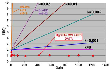
FIGURE 4-17 Excess noise factor plot for commonly used semiconductors for APDs. SOURCE: J. Beck, C. Wan, M. Kinch, J. Robinson, P. Mitra, R. Scritchfield, F. Ma, and J. Campbell, 2004, “The HgCdTeelectron avalanche photodiode,” Proc. SPIE 5564: 44.
For operation with eye-safe laser wavelengths of around 1.5 µm, InGaAs APDs with spectral sensitivity out to 1.7 µm are an attractive choice. They readily meet the bandwidth requirements needed for operation with pulses 1-10 ns wide. However, InGaAs APDs have a relatively high excess noise factor due to a hole to electron ionization coefficient ratio, k, of about 0.4, meaning that both holes and electrons will ionize significantly. For InAlAs, k = 0.2. Si, by comparison, has an ionization ratio of 0.02 and therefore much less excess noise, however it is not sensitive to wavelengths greater than 1.0 µm.
Figure 4-17 shows a plot of excess noise factor F(M), calculated using McIntyre’s equation,53 as a function of detector gain for various k values and for the common APD semiconductors. The k = 0 line with F(M) = 2 is based on McIntyre’s original theory for thick multiplication regions.54 HgCdTeelectron-initiated APD (e-APD) devices exhibit F(M) ~ 1,55 as shown for the measured data in Figure 4-17. Current theoretical modeling based on HgCdTe band structure explains the measured data.56
The excess carrier noise factor imposes a separate limit on the usable gain of an APD. In the limit of high avalanche gain, the sensitivity of an ideal noiseless APD is limited by the shot noise on the optical signal itself. However, most k ≠ 0 APDs generate multiplication noise in excess of the shot noise already present on the optical signal; this excess multiplication noise intensifies with increasing avalanche gain, such that for any given level of downstream amplifier noise, there is a limit to how much avalanche gain is useful. Increasing the avalanche gain beyond the optimal value increases the shot noise faster than the amplified signal photocurrent, degrading the signal-to-noise ratio.57
____________________
53 R.J. McIntyre, 1966, “Multiplication noise in uniform avalanche photodiodes,” IEEE Trans. Electron Devices, ED-13:164.; R.J. McIntyre, 1999, “A new look at impact ionization—Part I: A theory of gain, noise, breakdown probability and frequency response,” IEEE Trans Electron Devices 46: 1623.
54 Ibid.
55 J. Beck, C. Wan, M. Kinch, J. Robinson, P. Mitra, R. Scritchfield, F. Ma, J. Campbell, 2004, “The HgCdTe electron avalanche photodiode,” Proc. SPIE, 5564: 44.
56 M.A. Kinch, 2008, “A theoretical model for the HgCdTe avalanche photodiode,” J. Electron. Mater. 37: 1453.
57 G.M. Williams, D.A. Ramirez, M.M. Hayat, and A.S. Huntington, 2013, “Time resolved gain and excess noise properties of InGaAs/InAlAs avalanche photodiodes with cascaded discrete gain layer multiplication regions,” J. Appl. Phys. 113: 093705.
The tunable bandgap semiconductor Hg1-xCdxTe is the only commonly used semiconductor that exhibits k = 0 behavior and therefore the electron initiated avalanche multiplication exhibits close to ideal APD characteristic of excess noise factor F(M) = 1. Electron-initiated APD operation in Hg1-xCdxTe has been demonstrated for a broad range of compositions from x = 0.7 to 0.21, corresponding to cutoff wavelengths from 1.3 to 11 µm.58 Thus, HgCdTe at gain =100 provides 10 to 20 times less noise than InGaAs or InAlAs APDs and 4 times less noise than Si APDs.
In addition to APD operation in the linear mode, beyond the breakdown voltage Geiger-mode operation is realized and forms the basis for Geiger-mode APDs (GM-APDs), a technology widely used today for active sensing. GM-APDs are commonly based on Si, InGaAs and InGaAsP.59,60 They are being used as photon counting detectors in ladar systems and have been highly successful in 3-D imaging applications at 1.06 and 1.55 µm. Both Geiger and linear-mode APDs are discussed in greater detail below.
Superconducting niobium nanowire based single photon counting detectors have been demonstrated recently.61 This detector technology has been successfully used for some active sensing applications at 1.56 µm.62
In the following sections the various detector technologies in use are discussed as well as those that are expected to be developed in the next 5-10 years.
Single Element, Small Format Arrays, and Large Format Arrays
The choice of a detector for active EO sensing is strongly dependent on the kind application. Imaging 2-D lidar applications are discussed in Chapters 2 and 3.
Single-element Si PIN diodes and APDs suitable for the spectral range from 0.255 µm to 1.1 µm are commercially available and used for ranging applications such as with a pulsed 1.06 µm laser.63 The active area of a PIN ranges from diameters of 230 µm to 3.0 mm, and APDs have larger diameters, 5-16 mm. The Si APDs have a quantum efficiency (QE) of ≤40 percent at 1.06 µm and can be operated either in normal linear mode with an internal gain of 250 or more, or in Geiger-mode.64 These low-cost detectors are robust, immune to magnetic fields, and can be operated at or near room temperature.
____________________
58 J. Beck, C. Wan, M. Kinch, J. Robinson, P. Mitra, R. Scritchfield, F. Ma, and J. Campbell, 2006, “The HgCdTe electron avalanche photodiode,” J. Electron. Mater. 35: 1166.
59 B.F. Aull, A.H. Loomis, D.J. Young, R.M. Heinrichs, B.J. Felton, P.J. Daniels, and D.J. Landers, 2002, “Geiger-mode avalanche photodiodes for three-dimensional imaging,” MIT Lincoln Laboratory Journal 13: 335.
60 S. Verghese, K.A. McIntosh, Z.L. Liau, C. Sataline, J.D. Shelton, J.P. Donnelly, J.E. Funk, R.D. Younger, L.J. Mahoney, G.M. Smith, J.M. Mahan, D.C. Chapman, D.C. Oakley, and M. Brattain, 2009, “Arrays of 128 × 32 InP-based Geiger-mode avalanche photodiodes,” Proc. SPIE 7320: 73200M.
61 R.H. Hadfield, 2009, “Single photon detectors for optical quantum information applications,” Nature Photonics 3(12): 696.
62 A. McCarthy, N.J. Krichel, N.R. Gemmell, X. Ren, M.G. Tanner, S.N. Dorenbos, V. Zwiller, R.H. Hadfield, and G.S. Buller, 2013, “Kilometer-range, high resolution depth imaging via 1560 nm wavelength single-photon detection,” Optics Express 21(7): 8904.
63 See http://voxtel-inc.com/products/.
64 M.A. Krainak, X. Sun, G. Yang, L.R. Mikoc, and J.B. Abshire, 2009, “Photon detectors with large dynamic range and at near infrared wavelength for direct detection space lidars,” Proc. of SPIE 7320: 732005.
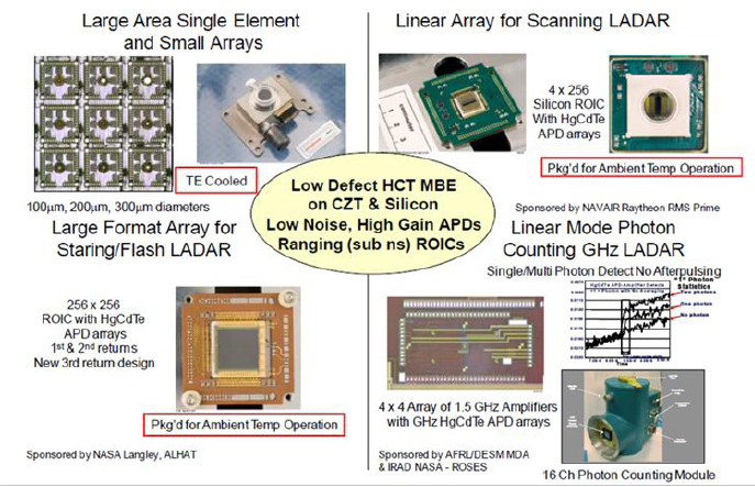
FIGURE 4-18 Family of HgCdTe APD detectors in a variety of formats. SOURCE: M. Jack, G. Chapman, J. Edwards, W. McKeag, T. Veeder, J. Wehner, and F. Amzajerdian, 2012, “Advances in LADAR Components and Subsystems at Raytheon,” Proc. of SPIE 8353: 83532F-1.
A variety of pixel format detector arrays have been developed for a wide range of applications. Figure 4-18 shows detectors in multiple formats from single pixels to 256 × 256 arrays for various ladar applications. No single format is suitable for all classes of applications. For example, for gas-sensing lidar applications, small detector formats are well suited, but they need to be sensitive in the wavelength region for the specific gases.65 For 3-D topographic mapping, larger formats are preferred to maximize ground surface area per unit time and to reduce reliance on mechanical scanners.
There are two main types of detectors that are sensitive to single photons, Geiger-mode (GM) and linear mode (LM). Both rely on avalanche multiplication of the carrier generated by the incident photon so that noise in ROIC can be overcome. Avalanche of carriers occurs under high electric field when accelerated carriers impact the lattice to create more carriers, which are subsequently accelerated and have the opportunity to impact ionize. Both electrons and holes can ionize at rates that are dependent on the fundamental properties of the semiconductor material. The two modes are different in the magnitude of the avalanche multiplication that is created.
____________________
65 J. Beck, J. McCurdy, M. Skokan, C. Kamilar, R. Scritchfield, T. Welch, P. Mitra, X. Sun, J. Abshire, and K. Reiff, 2013, “A highly sensitive multi-element HgCdTe e-APD detector for IPDA lidar applications,” Proc. of SPIE 8739: 87390V.
Geiger-Mode APDs
Geiger-mode avalanche photodiode detectors (GM-APDs) are biased at voltages several volts above the breakdown voltage, typically much higher than biases of linear-mode detectors. At this high voltage a metastable state is reached where carriers generated through photon absorption (or dark) entering the depletion region begin avalanche multiplication and cause a sustained chain of impact ionizations, resulting in a measurable current pulse. Materials with high probabilities of electron or hole ionization are usually good for Geiger-mode detectors. The current generation of GM-APDs with single-photon-counting sensitivity were developed at MIT’s Lincoln Laboratory (MIT-LL).66,67Figure 4-19
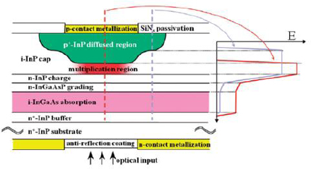
FIGURE 4-19 Geiger-mode detector architecture from Princeton Light wave.
SOURCE: M.A. Itzler, M. Entwistle, M. Owens, X. Jiang, K. Patel, K. Slomkowski, T. Koch, S. Rangwala, P.F. Zalud, Y. Yu, J. Tower, J. Ferraro, 2009, “InP-based Geigermode avalanche photodiode arrays for three-dimensional imaging at 1.06 µm,” Proc. of SPIE 7320, 73200O.
shows the architecture of a GM-APD device based on lattice matched In0.53Ga0.47As, with a bandgap of ~0.75 eV (1.65 µm cutoff at 300 K), grown on InP substrate, that is suitable for detection at ~1.5 µm.68,69 In this backside-illuminated detector architecture the laser photon absorption occurs in the narrower bandgap InGaAs layer, and the resulting photo excited holes are injected into the high-field InP multiplication region70. Operating at temperatures ≤200 K the dark current in this device is dominated by the generation-recombination current in the InGaAs absorber layer.
The GM-APD is a noiseless gain detector with nearly infinite gain and a well-designed device is essentially shot noise limited. The detectors show 1 ns or less timing performance. The dark count rates are typically ~10 kHz and photon detection efficiency (PDE) is ~30 percent. These devices have to be
____________________
66 B.F. Aull, A.H. Loomis, D.J. Young, R.M. Heinrichs, B.J. Felton, P.J. Daniels, D.J. Landers, 2002, “Geigermode avalanche photodiodes for three-dimensional imaging,” MIT Lincoln Laboratory Journal 13: 335.
67 S. Verghese, K.A. McIntosh, Z.L. Liau, C. Sataline, J.D. Shelton, J.P. Donnelly, J.E. Funk, R.D. Younger, L.J. Mahoney, G.M. Smith, J.M. Mahan, D.C. Chapman, D.C. Oakley, and M. Brattain, 2009, “Arrays of 128x32 InPbased Geiger-mode avalanche photodiodes,” Proc. SPIE 7320: 73200M.
68 M.A. Itzler, M. Entwistle, M. Owens, X. Jiang, K. Patel, K. Slomkowski, T. Koch, S. Rangwala, P.F. Zalud, Y. Yu, J. Tower, and J. Ferraro, 2009, “InP-based Geiger-mode avalanche photodiode arrays for three-dimensional imaging at 1.06 µm,” Proc. of SPIE 7320: 73200O.
69 M. Entwistle, M.A. Itzler, J. Chen, M. Owens, K. Patel, X. Jiang, K. Slomkowski, and S. Rangwala, 2012, “Geiger-mode APD camera system for single photon 3-D LADAR imaging,” Proc. of SPIE 8375: 83750D.
70 M.A. Itzler, M. Entwistle, M. Owens, X. Jiang, K. Patel, K. Slomkowski, T. Koch, S. Rangwala, P.F. Zalud, Y. Yu, J. Tower, and J. Ferraro, 2010 “Design and performance of single photon APD focal plane arrays for 3-D LADAR imaging”. Proc. SPIE 7780:77801M, Detectors and Imaging Devices: Infrared, Focal Plane, Single Photon.
reset after photon detection because of a holdoff time, also called the dead time, during which the detectors are blinded. This issue can be mitigated by spreading the signal over multiple pixels to reduce the probability of a photon striking a blinded pixel.
A GM-APD FPA is illustrated in Figure 4-20. They are fabricated by In bump bonding to ROICs designed to enable 3-D imaging. A lenslet array is mounted on the detector array to focus the incident light onto an array of APDs and thereby improve the detector fill factor. They also increase the signal when small junctions are used to reduce leakage current. Geiger-mode operation of the APD involves momentarily biasing the diode voltage above its avalanche breakdown voltage71. In this metastable state, a single photon can trigger a signal large enough to trigger complementary metal oxide semiconductor (CMOS) circuitry in the ROIC unit cell. Digitization of the signal is performed in the unit cell. The unit cells also accurately clock the time of arrival for each pixel and then disarms the APD. After the CMOS circuit disarms the APD, it must wait for a reset time of 1-2 µs until the trapped holes are thermally ionized and can escape. Only at that point is the device ready to be re-armed, without it immediately after-pulsing, and to receive the next photons.
In the GM-APD, regardless of the number of photons incident at a given time, the signal level is the same. When intensity information is required, the histogram of hits over a period of time is measured. For 3-D imaging, multiple range returns on a pixel are handled using multiple pulses. The ROICs can be designed for linear-mode ladar or for continuous sensing for coherent mode operation.
GM-APD devices are commercially available in the United States from Princeton Lightwave and from Boeing Spectrolab in 32 × 32 and 32 × 128 pixel formats. Recently 64 × 256 formats were demonstrated at MIT-LL.72 Overall, GM-APDs are the more mature detector technology currently in use for 3-D imaging with photon counting sensitivity. They have been used for 3-D imaging applications in a variety of environments but primarily in airborne settings.
The layout for a typical GM-APD camera system consists of FPAs packaged on thermoelectric coolers (TECs) and ceramic carriers with microlenses above the FPA, as shown in Figure 4-21. Frame rates of 186 kHz have been reported and are scaleable up to 300 kHz with appropriate range gates. Range gates are selectable in increments of 2, 4, 8 and 10 µs. Timing is captured digitally with a phase-lockedloop master clock and 13 bits of resolution.
Linear/Proportionate-Mode APDs
Linear-mode APD devices have been most commonly fabricated from Si, InGaAs and HgCdTe. Linear Si APD technology is mature and widely available. Sensitivities to single-photon counting have been demonstrated below the breakdown voltage of ~ 250 V.73
____________________
71 G. M. Williams, “GHz-rate Single Photon Sensitive Linear Mode APD Receivers” Available at http://voxtelinc.com/files/2012/07/GHz-rate-Single-Photon-Sensitive-Linear-Mode-APD-Receivers-SPIE-Winter-2009-.pdf.
72 S. Verghese et al., 2007, “Arrays of InP-based avalanche photodiodes for photon counting,” IEE Journal of Selected Topics in Quantum Electronics 13(4): 870.
73 X. Sun, 1992, “Photon counting with silicon avalanche photodiodes,” J. Lightwave Technol. 10: 1023.
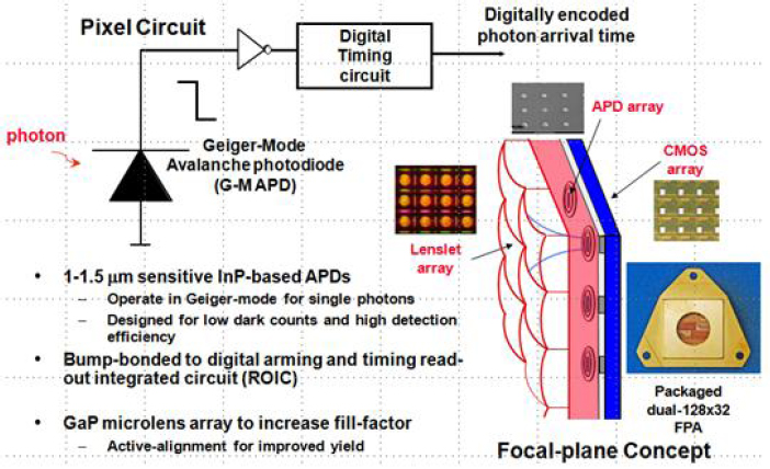
FIGURE 4-20 Geiger-mode sensing concept. SOURCE: Melissa Choi, MIT-LL.
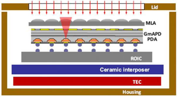
FIGURE 4-21 GM-APD camera packaging. SOURCE: M. Entwistle, M.A. Itzler, J. Chen, M. Owens, K. Patel, X. Jiang, K. Slomkowski, and S. Rangwala, 2012, “Geiger-mode APD Camera System for Single Photon 3-D LADAR Imaging,” Proc. of SPIE 8375: 83750D.
InGaAs-based APDs
Linear-mode InGaAs APDs are commercially available in a variety of formats ranging from single pixel to 128 × 128 FPAs. As discussed above, due to the high k value of 0.4 the usable gain of conventional InGaAs is limited to ~10. To overcome this limitation, a multi-gain-stage linear-mode InGaAs single-carrier multiplication (SCM) APD has been developed at Voxtel, Inc.,74,75 that allows single photon noise equivalent input (NEI) sensitivity when coupled to a custom ROIC.76 The key innovation here is a method to increase the gain at which low-noise multiplication can be achieved.
According to Williams et al. “the APD is grown by molecular beam epitaxy on InP substrates from lattice-matched InGaAs and InAlAs alloys. Avalanche multiplication inside the APD occurs in a series of asymmetric gain stages whose layer ordering acts to enhance the rate of electron-initiated impact ionization and to suppress the rate of hole-initiated ionization when operated at low gain. The multiplication stages are cascaded in series, interposed with carrier relaxation layers in which the electric field is low, preventing avalanche feedback between stages. These measures result in lower excess multiplication noise and stable linear-mode operation at higher avalanche gain than are characteristic of APDs fabricated from the same semiconductor alloys in bulk. The noise suppression mechanism is analyzed by simulations of impact ionization spatial distribution and gain statistics. The devices employing this design have been demonstrated to operate at linear-mode gain in excess of 6,000 without avalanche breakdown. The usable APD gain achieved is 10-45. Excess noise characterized by an effective impact ionization rate ratio below 0.04 has been reported at gains over 1,000”.77
The detector arrays are fabricated as backside illuminated (through the InP substrate), mesaetched diodes with 7 to 10 gain stages to provide a QE of 85 percent across the 950 to 1,650 nm spectral band. The ROIC operates at a 10 kHz frame rate, enables less than 200 ps time jitter and 3 ns pulse pair resolution by using a low-noise GHz-class preamplifier. The hybridized FPAs, in 32 × 32 and 128 × 128 pixel formats with 36-42 µm pixel pitch, are capable of time stamp and amplitude sample of the first three or the first and last pulse returns. The device operates at 230 K. Figure 4-22 shows an example.
HgCdTe APDs
The Hg1-xCdxTe material system is a solid solution of CdTe (Eg=1.6 eV at ~0 K) and HgTe (Eg= -0.3 eV at ~0 K), where the bandgap is tunable between these extremes asxis varied from 0 to 178. Despite the wide tunability in bandgap and therefore the detector cutoff wavelength, the lattice constant changes little with the x value. As a consequence HgCdTe structures with different bandgaps can be grown on the same lattice-matched substrate, which is typically Cd0.96 Zn0.04Te.
____________________
74 G.M. Williams, D.A Ramirez, M.M. Hayat, and A.S. Huntington, 2013, “Time resolved gain and excess noise properties of InGaAs/InAlAs avalanche photodiodes with cascaded discrete gain layer multiplication regions,” J. Appl. Phys. 113: 093705.
75 See http://voxtel-inc.com/products/.
76 A.S. Huntington, M.A. Compton, and G.M. Williams, 2007, “Linear-mode single-photon APD detectors,” Proc. SPIE 6771: Q7710.
77 Ibid
78 J. Beck, C. Wan, M.Kinch, J. Robinson, P. Mitra, R. Scritchfield, F. Ma, J. Campbell, 2004, “The HgCdTe Electron Avalanche Photodiode,” Proc. SPIE, 5564: 44.
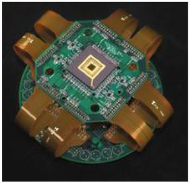
FIGURE 4-22 A 32 × 32 element InGaAs SCM-APD shown mounted with drive electronics. SOURCE: http://voxtel-inc.com/products/.
One of the commonly employed HgCdTe electron-initiated APD architectures, the front-side-illuminated, cylindrical geometry, lateral collection, p-around-n device geometry is illustrated in Figure 4-22. This particular device architecture used at DRS Technologies is called High Density Vertically Integrated Photodiode (HDVIP®).79,80 The HDVIP structure with HgCdTe grown by liquid phase epitaxy (LPE) is currently employed in MWIR and LWIR staring FPAs in production at DRS. The key features of this architecture are: “(1) interdiffused CdTe passivation of both surfaces for low 1/f noise, (2) thermal cycle reliability that is detector and array size independent, (3) low defects due to diode junction orientation being orthogonal to the direction of threading dislocations, and (4) front-side illumination for high quantum efficiency from the IR into the visible region as shown in Figure 4-23, and good modulation transfer function (MTF)”81.
For APD operation the reverse bias is increased until an electric field sufficient for avalanche multiplication is achieved. At a few volts bias, the n-doped region becomes fully depleted. Photoelectrons generated in the p-doped region diffuse to the n region, which is the multiplication region. Multiplication occurs as the electrons traverse the high-field depletion region shown Figure 4-24. A unique feature of the HgCdTe e-APD is that holes generated in the multiplication region, for all practical purposes, do not
____________________
79 J. Beck, C. Wan, M.Kinch, J. Robinson, P. Mitra, R. Scritchfield, F. Ma, J. Campbell, 2004, “The HgCdTe Electron Avalanche Photodiode,” Proc. SPIE, 5564: 44.
80 J. Beck, C. Wan, M. Kinch, J. Robinson, P. Mitra, R. Scritchfield, F. Ma, and J. Campbell, 2006, “The HgCdTe Electron Avalanche Photodiode,” IEEE LEOS Newsletter, 8 (October).
81 P. Mitra, J. D. Beck, M. R. Skokan,; J. E. Robinson,; J. Antoszewski,; K. J. Winchester,; A. J. Keating,; T. Nguyen, K. K. M. B. D. Silva, C. A. Musca, J. M. Dell, L. Faraone, 2006, “SWIR hyperspectral detection with integrated HgCdTe detector and tunable MEMS filter” Proc. SPIE 6295:62950G, Infrared Detectors and Focal Plane Arrays VIII.
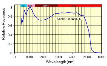
FIGURE 4-23 Broad spectral response from visible to MWIR is characteristic of front-side-illuminated HDVIP e-APD. SOURCE: DRS Technologies, Dallas Texas.
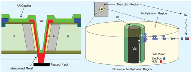
FIGURE 4-24 Schematic of a single-element HgCdTe e-APD based on the lateral collection p-around-n geometry. SOURCE: DRS Technologies, Dallas, Texas.
multiply, which results in an ideal k = 0 APD, where k is the hole to electron ionization coefficient ratio. Another unique feature of the HgCdTe e-APD is that the multiplication process is largely deterministic, which results in an excess noise factor near 1.0. The geometry favors high mobility electron injection into the central high-field region, which helps achieve high bandwidth. The geometry and the 3-5 µm thick HgCdTe layer makes the shunt capacitance of each diode extremely small, typically 6 to 12 fF per diode, which reduces the ROIC preamplifier noise and maintains a wide electrical bandwidth.
The noiseless gain behavior of the HgCdTe e-APD is illustrated in Figure 4-25. It is a 4.5 µm cutoff e-APD operating at 85 K with a 1.2-1.8 µm cold filter and illuminated with a 1.55 µm, 10 ns pulsewidth laser with 800 photons incident on the 64 µm pitch detector. The plot shows the effect of the detector gain achieved as a function of bias voltage on the left. At bias voltages of <1 V, where most HgCdTe photodiodes for passive mode are operated, there is no signal corresponding to the incident laser photons. As the bias voltage is raised to 4 V corresponding to an APD gain of ~5 the signal is barely discernible, while at 8 V the gain is ~180 and the SNR is ~45. At 10 V it reaches a gain of ~700 and a SNR of 90 and the detector becomes shot noise limited.
These characteristics of HgCdTe have spawned a large effort in the development of e-APDs. Detector gains of well over 1000 have been demonstrated. Detectors across the 1.7-11 µm spectral band have been fabricated, some in array formats as large as 640 × 480 pixels with 25 µm pitch and integrated in active imaging systems. Linear-mode HgCdTe e-APD devices have been realized in several device
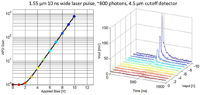
FIGURE 4-25 Effect of noiseless gain. Left: APD gain vs. applied bias on a HgCdTe detector at 80 K incident with 800 photons in 10 ns, 1.55 µm pulses. Right: oscilloscope traces of the signal output taken at various applied bias voltages. The colored data points on the left correlate with the same colored traces on the right. SOURCE: DRS Technologies, Dallas, Texas.
architectures, grown by liquid phase epitaxy (LPE) and molecular beam epitaxy (MBE), in the United States and Europe.82- 87 Detectors and FPAs have been demonstrated for single-photon counting,88,89,90 active-passive imaging,82 and 3-D imaging applications.91
____________________
82 W. McKeag, T. Veeder, J. Wang, M. Jack, T. Roberts, T. Robinson, J. Neisz, C. Andressen, R. Rinker, T.D. Cook, and F. Amzajerdian, 2011, “New developments in HgCdTe APDs and LADAR receivers,” Proc. of SPIE 8012: 801230.
83 J. Beck, M. Woodall, R. Scritchfield, M. Ohlson, L. Wood, P. Mitra, and J. Robinson, 2008, “Gated IR imaging with 128x128 HgCdTe electron avalanche photodiode FPA,” J. Electron Mater. 37: 1334.
84 A. Ashcroft and I. Baker, 2010, “Developments in HgCdTe avalanche photodiode technology and applications,” Proc. of SPIE 7660: 76600C.
85 J. Rothman, “APD Development at CEA Leti-Minatec, 2009, “ESO Detectors for Astronomy Workshop proc. Available at http://www.eso.org/sci/meetings/dfa2009/program.html.
86 E. deBorniol, J. Rothman, F. Guellec, G. Vojetta, G. Destéfanis, 2012, “Active three-dimensional and thermal imaging with a 30-µm pitch 320 × 256 HgCdTe avalanche photodiode focal plane array,” Optical Engr. 51: 061305.
87 O. Gravrand, G. Destefanis, S. Bisotto, N. Baier, J. Rothman, L. Mollard, D. Brellier, L. Rubaldo, A. Kerlain, and M. Vuillermet, 2013, “Actual issues in HgCdTe research and expected progress in IR detector fabrication,” J. Electron. Mater. 42(11):3349.
88 J.D. Beck, R. Scritchfield, P. Mitra, W. Sullivan III, A.D. Gleckler, R. Strittmatter, and R.J. Martin, 2011, “Linear mode photon counting with the noiseless gain HgCdTe e-APD,” Proc. of SPIE 8033: 80330N.
89 M.L. Bryan, G. Chapman, D.N.B. Hall, M.D. Jack, S.M. Jacobson, and J. Wehner, 2012, “Investigation of linear-mode, photon-counting HgCdTe APDs for astronomical observations,” Proc. of SPIE 8453: 84532F.
90 G. Vojettaa, F. Guelleca, L. Mathieua, K. Fouberta, P. Feautrierb, and J. Rothman, 2012, “Linear photoncounting with HgCdTe APDs,” Proc. of SPIE 8375: 83750Y.
91 E. deBorniol, J. Rothman, F. Guellec, G. Vojetta, and G. Destéfanis, 2012, “Active three-dimensional and thermal imaging with a 30-µm pitch 320 × 256 HgCdTe avalanche photodiode focal plane array,” Optical Engineering 51: 061305.
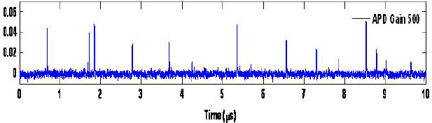
FIGURE 4-26 Analog output showing single photon initiated events captured with a 4,330 nm cutoff HgCdTe detector at 84 K. SOURCE: J.D. Beck, R. Scritchfield, P. Mitra, W. Sullivan III, A.D. Gleckler, R. Strittmatter and R.J. Martin, 2011, “Linear mode photon counting with the noiseless gain HgCdTe e-APD,” Proc. of SPIE 8033:80330N.
The linear gain and low excess noise not only allow detecting single photon events, they also enable proportional photon counting with a greatly enhanced dynamic range. Gain above 500 is readily achieved, which is high enough for single photon detection when integrated with a low noise ROIC.92 The minimum time between distinguishable events less than 10 ns has been reliably demonstrated. Figure 4-26 shows high-speed oscilloscope traces of spikes of single and multiple photon-initiated events obtained from the analog output of the detector at a gain of 500 and SNR ~14. The spectral response of the detector shows a high QE from 400 nm in the visible to the 50 percent cutoff wavelength at 4,330 nm in the MWIR.
The key attributes of the linear-mode HgCdTe, photon-counting, electron-initiated APD may be summarized as follows:
• No after-pulsing effects
• Ability to resolve photons that are closely spaced in time
• Ability to measure the number of photons in a multiphoton pulse
• Ultrahigh dynamic range: ability to run in photon counting mode at low flux levels and to transition seamlessly to ordinary linear mode at higher flux levels
• Broad and tunable spectral range offered by HgCdTe, and
• Photon detection efficiency of ≥50 percent
Linear-mode APDs performance data for several device architectures are tabulated in Table 4-2. The table compiles data from various sources taken under different conditions and therefore cannot be directly compared. Instead each column should be considered in a stand-alone manner. This table is by no means a complete or an exhaustive list of data from all the organizations; rather it presents the state of the art for specific device architectures.
Comparison of Linear-Mode and Geiger-Mode APDs
A direct apples-to-apples comparison of the performance of linear-mode and Geiger-mode APDs for active sensing applications is relatively complex and is best addressed based on individual applications and at the sensor level. Each approach has its own advantages and disadvantages, so in designing a receiver, the beneficial characteristics of each approach are leveraged to maximize sensor
____________________
92 J.D. Beck et al., op. cit.
TABLE 4-2 Performance Parameters of Various Linear-mode APD Photon Detectors
| Device Parameter | Si Arpad | HgCdTeb | HgCdTec,d | InGaAsa | InAlAse |
| QE (percent) | 35 at 1.06 µm | >90 at 1.06 µm (no ARC) | 83 at 1.55 µmf | 80 | 80 at 1.06 µm |
| Detector cutoff (µm) | 1.1 | 4.3 | 1.2/1.2 | ||
| Bandwidth (MHz) | 140 | 500 (est.) | 120g | 100-1000 | >1000 |
| k (ionization ratio) | 0.008 | 0 | 0 | 0.15 | |
| Excess Noise factor | 3 | 1 | 1.3-1.4 | TBD | 8 (est. for k=0.15; M=45) |
| Gain M | 120 | 200-350 | 468 | 30 | 45 |
| Dark Current (pA) | 50 | 0.5 | 1 | ||
| Bias (V) | 16 | 13 | 71/82.5 | ||
| NEP (fW/rt-Hz) | 30 | 7-25 (at gain =100) | 0.5 | 81 | 150/250 |
| Dynamic Range (dB) | >20 | > 30 | 22 | ||
| Pixel format | Single pixel | 4 × 4 | 2 × 8 64 × 64 µm pix | Single pixel | Single/16 channel |
| Pixel area µm | 700 (dia.) | 64 × 64 | 200 (dia.) | 75/100 (dia.) | |
| Operating temperature (K) | 300 | 101-120 | 84 | 300 | 300 |
a Krainak et al., 2009, “Photon detectors with large dynamic range and at near infrared wavelength for direct detection space lidar,” Proc. of SPIE 7320: 732005-1.
b Wang et al., 2011, “n-on-p vertical architecture SAM design,” Proc. of SPIE San Diego, CA, Aug.21-25.
c Beck et al., 2011 “Linear mode photon counting with the noiseless gain HgCdTe e-APD,” Proc. SPIE, 8033:80330N.
d Gleckler et al, 2012, “Application of an end-to-end linear mode photon counting (LMPC) model to noiseless-gain HgCdTe APDs,” Proc. Of SPIE 8033: 1.
e Bai et al., 2012, “16 channel GHz low noise SWIR photoreceivers”, Proc. of SPIE, 8353: 83532H-3.
f At unity gain flood illuminated. “QE percent” = QE*FF*eCE (quantum efficiency in active area 98 percent × fill factor 97 percent × electron collection efficiency 86.8 percent). Responsivity(e/ph) = QE*Gain.
g BW of Detector/ROIC.
performance. For example, detector or sensor performance comparison at the “per pulse” level could be misleading because in the linear mode, a single pulse to “detect” at low pulse repetition frequency (PRF) would compare with multiple pulses to “detect” at high PRF in the Geiger-mode.
For the case of photon-counting ladar, a systematic comparison between the two approaches based on statistical modeling has been reported.93 The key conclusions that can be drawn from the study of Holmos et al. are the following:
• For the same low noise levels obtained in LM-APD as in GM-APD, a comparable ladar performance is expected.
• Under conditions of obscuration, GM-APD approaches the performance of LM-APD by increasing the number of pulses.
____________________
93 M.J. Halmos, R.A. Reeder, B. Boland, J.P. Bulot, and M.J. Klotz, 2011, “Photon counting ladar,” available at http://sti.usra.edu/clrc2011/presentations/Session%204/Summary%20M%20Halmos.pdf.
• For fast-moving targets or when the measuring time or the measuring number of pulses is limited, LM-APD may have an advantage over GM-APD, depending on the speed of the target.
• Intensity measurements in LM-APDs can be performed with fewer pulses than in GM-APDs.
• The ROIC unit cell circuit for LM-APD is considerably larger than for GM-APD, which may limit the pixel pitch in future arrays.
For fast moving targets, the linear mode can collect the image in one pulse with no concern about smear, but one concern for the Geiger-mode system is that the image will smear over the multiple pulses required for the “frame.” In the aggressive case where 1000 pulses are needed to make an image (such as in an intensity image with multiple ranges per posting) at 100 kHz, the time required to collect an image is 10 msec. During this time, the angular rate that smears one pixel is 1 deg/sec, which can easily be corrected in processing using the output of an inexpensive gyro. The target velocity that smears one pixel (calculated as the resolution divided by the collection time (20 cm/10 ms)) is 20 m/s or 44 mph, so the Geiger-mode system could effectively image most ground vehicles in this regime. In more typical cases requiring 10 to 100 pulses to make an image, the image acquisition time would be even faster.
Note that different assumptions about the characteristics of the APDs (e.g., higher frame rate for the linear-mode APD, different sensitivity assumptions, etc.) and the sensors will change the results described above. A complete discussion of the trades between the two types of systems requires a detailed technical analysis and robust framework for comparison, which is beyond the scope of this report.
Both linear-mode and Geiger-mode APDs have been used for coherent-mode ladar. Coherent-mode detectors, which work by beating a local oscillator with the returning pulse in an active sensor, can provide information on the target reflecting the laser pulse. Some of the comparisons between the various technologies are illustrated in Table 4-3.
Geiger-Mode Detector Summary
• Dark count rate 1-10 kHz for thermoelectric (TE) cooled operation (263-300 K), array results reported with 33-37 percent photon detection efficiency (PDE).
• 64 × 256 array is currently the largest.
• Jitter of 135 ps.
• Primarily 1.06 µm, can perform at 1.55 µm and 2.4 µm with a trade off in DCR.
• Crosstalk <1 percent to adjacent pixels.
• <1 ns time resolution.
• Pros
– Single photon sensitivity,
– Sub-nanosecond timing information,
– Direct photon-to-digital conversion on the focal plane, low noise readout,
– Scalable to larger arrays,
– High bandwidth (~GHz),
– TE-cooled operation,
– Compatible with direct and coherent sensing,
– Extensive 3-D imaging results, and
– Mature, fielded and commercially available technology.
• Cons
– 1 µsec reset time required to avoid afterpulsing, and
– Saturation flux ~1 x 10⁹ photons/sec for typical arrays.
TABLE 4-3 Performance Parameters Comparison of Linear Geiger and Coherent Mode Detectors
| Parameter | Linear | Geiger | Coherent |
| Dark count rate | Critical target <104 | Critical target <104 | Not critical |
| Idark overcome by LO | |||
| Spectral range | NIR – LWIR | NIR – SWIR | NIR – LWIR (Linear) |
| Bandwidth | GHz | GHz | GHz |
| Multipulse resolution on a single pixel | Nanoseconds | Microseconds Dead time from after-pulsing | Nanoseconds |
| Intensity | Yes (single pulse) | No (single pulse) Yes with multipulse statistics | Yes (single pulse linear) |
| Sensitivity limit | Subphoton | Subphoton | One photon |
| Probability of return detection | QE x Pgain x Pamp > 80% | QE x Pgain x Pamp 30-50% trade with Idark | QE x fLO x Pamp > 80% with enough LO |
| Radiation hardening | High | Low | High |
| Focal plane power | Moderate to high | Low | High (LO on FPA) |
| Laser constraints | Minimal Odd pulse shapes and variable amplitudes OK | High rep rate required Need to adjust power to achieve subphoton laser returns | Severe High beam quality and alignment needed |
| Operating temperature | Ambient – 80 K trade DCR | Ambient – 200 K | Ambient – 80 K |
| ROIC complexity | High | Moderate | High |
SOURCE: M. Jack, J. Wehner, et al., personal communication (2013).
Linear-Mode Detector Summary94
• Single photon sensitivity demonstrated.
• 6 nW MDS at 300 K 256 × 256 demonstrated (NEP~ 0.4 nW).
• Operability >95 percent.
• NEI < 0.5 photons at 80 K.
• NEP < 0.1 nW at 80 K.
• 1.5 GHz bandwidth demonstrated.
• Gains 100-1000 (at 80 K) for SWIR and up to 8000 for MWIR (at 80 K) demonstrated.
• DCR of 10-20 kHz at 150 K demonstrated.
• Fex <1.05 measured.
• Gain uniformity 3 percent.
• 12 e/s dark current at M=24.
• 320 × 256, 30 µm pitch ROIC 1.5 kHz Passive/Gated active readout.
____________________
94 Based on results from different groups.
• Jitter < 100 ps.
• 1024 × 768, 20 µm pitch gated mode ROIC, 256 × 256 w/ 300 kV/A 100 MHz flash ROIC
• Pros
– HgCdTe excess noise factor ~1.
– MBE growth or LPE for HgCdTe.
– Trades QE against Jdark (DCR).
– Bandwidth.
– Tunable gain.
– Design flexibility with cutoff wavelength.
– Compatible with linear mode and coherent sensing.
– High bandwidth designs to 4.5 GHz.
• Cons
– Sensitive to surface passivation.
– MBE typically has higher defect rate than LPE.
– ROIC more complex.
– Under development.
Linear-mode APD arrays have very low detector reset time hence much less dead time, about 2-3 orders of magnitude shorter than current GM-APD technology. Since the aperture efficiency (number of photons detected versus the number of photons at the aperture) of GM-APDs is low, the target information is accumulated statistically from a multitude of laser shots.
High-gain linear-mode APDs have the ability to measure signal amplitude information, providing additional target information to support image processing and analysis. These traits reduce the laser power and number of shots and maximize the aperture efficiency of the system.
Geiger-mode APD arrays form the basis of 3-D imaging systems that are far more mature than those based on linear-mode staring arrays. GM-APDs have been successfully deployed in multiple missions as part of the Airborne Ladar Imaging Research Testbed (ALIRT) and High Altitude Lidar Operational Experiment (HALOE) systems.
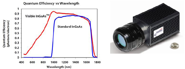
FIGURE 4-27 Left: Spectral response of In0.53Ga0.47As photodiodes grown on InP. Right: Camera based on a 640 × 480 FPA. Right: Camera based on a 640 × 480 FPA. SOURCE: UTC-Goodrich.
Framing cameras are used for digital holography and polarization-based flash 3-D ladar. These are conventional passive FPAs, built with gated imaging capability in the ROIC. The FPAs are widely available from the visible to the LWIR wavelengths. In the visible both charge-coupled device(CCD) and CMOS-based imagers are available in the multimegapixel to tens of megapixel formats.
For commonly used ladar laser wavelengths of 1.06 and 1.57 µm cameras using InGaAs FPAs are available. The highest performing FPAs in this class are based on lattice matched In0.53Ga0.47As grown on InP substrates. These backside illuminated (through the InP substrate) FPAs have sensitivity over the 0.9-1.7 µm band. The long wavelength end is limited by the bandgap of the InGaAs, while the short wavelength end is limited by the absorption in InP. The latter can be extended into the visible by removing the InP substrate. The quantum efficiency, however, falls off rapidly between 0.9 and 0.5 µm as shown in Figure 4-27.
Standard versions of the InGaAs FPAs are commonly in the 640 × 512, 25 µm pitch pixel format. Higher resolution versions are available in 1.3-megapixel format with 1,280 × 1,024 pixel and 12.5 µm pitch that operate at frame rates of 30 Hz. Depending on the required sensitivity, the FPAs are TE-cooled or operated at room temperature. The sensitivity achieved in these cameras in terms of NEI is between 1 and 2 × 10⁹ photons/cm2-s.
As longer wavelength lasers become more available and more popular for ladar applications such as those at ~2 µm and longer, detector arrays with longer cutoff wavelength are needed. Such arrays with varying cutoff wavelengths from the MWIR band to the LWIR in large array formats are increasingly available. The arrays with high sensitivity and integrated with high f-number optics require cooling to ≤150 K.
In the MWIR band, InSb FPAs as large as 8 K × 8 K have been reported (L-3 Cincinnati Electronics) with 10-12 µm pixel pitch.95 In the LWIR and MWIR bands HgCdTe FPAs 1280 × 720 format with 12 µm pitch are available, and a 4K × 4K HgCdTe array has been demonstrated by Raytheon.
Owing to wide spectral response of the front-side-illuminated HgCdTe detectors (Figure 4-21), detector arrays fabricated with MWIR cutoff can also be used in the SWIR band by employing appropriate cold filters. An example of MWIR and SWIR imagery obtained with a 640 × 480, 12 µm pixel pitch format HgCdTe MWIR FPA is shown on the left in Figure 4-28. The camera operates at a frame rate of 60 Hz with the FPA maintained at 150 K. The noise equivalent temperature difference (NETD) measured in the MWIR band with 4 degree horizontal FOV is ~25 mK.
Most recently, cameras with 1,280 × 720 HgCdTe LWIR FPAs have been demonstrated with pixel pitches of only 5 µm at DRS with DARPA sponsorship.96 This is the first detector array with a pixel pitch smaller than the detection wavelength (Nyquist limit). Similar format arrays have been developed in the MWIR band as well. These front-side-illuminated devices have broad spectral response and can be used in the MWIR and SWIR bands.
Gated Cameras
Range-gated imaging is performed primarily in the SWIR band with a 1.55 µm or 1.06 µm laser. In Chapter 2 this was described as 2-D imaging. This section describes two range-gated imaging technology approaches: one that has been in use for a few years now and another that was developed more recently.
____________________
95 M.R. Kruer, 2012, “Infrared sensors for navy applications,” keynote address presented at 2012 U.S. Workshop on the Physics and Chemistry of II-VI Materials, Nov. 27-29, Seattle, Washington.
96 N. Dhar and R. Dat, 2012, “Advanced imaging research and development at DARPA,” Proc. SPIE 8353: 835302.
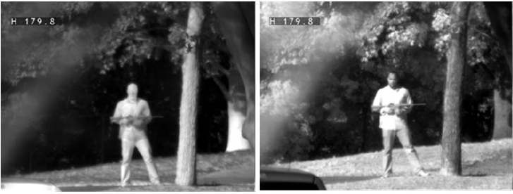
FIGURE 4-28 MWIR (left) and SWIR (right) imagery taken with a 640 × 480, 12 µm pixel camera operating at 150 K. SOURCE: DRS Technologies, Dallas, Texas.
The first of these is the Electron Bombarded Active Pixel Sensor (EBAPS), based on a GaAs or InGaAs photocathode in proximity focus with a high resolution, CMOS Active Pixel Sensor (APS) imager anode.97 The SWIR version of this TE-cooled sensor has a spectral response that ranges from 950 to 1,650 nm. Electrons emitted by the photocathode are directly injected in the electron bombarded mode into the anode. Low noise gain is achieved in the CMOS anode by conversion of the high energy photoelectron (resulting from 1-2 keV bias applied between the photocathode and CMOS anode) to electron-hole pairs in the anode via the electron bombarded semiconductor (EBS) gain process. The electrons are collected in the anode pixel and subsequently read out. The EBS gain process is inherently low noise with an excess noise factor of less than 1.1.
Intevac’s gated imaging sensor uses a 640 × 480 format, 13.4 µm pitch (with pixels binned at 2 × 2) FPA with QE of ≤20 percent at 1.55 µm. It has a minimum gate width of ~70 ns and a gate rise and fall time of 65 ns. SOURCE: http://www.intevac.com/wp-content/uploads/2012/01/LIVAR-M506-Datasheet1.pdf.
A second, more recent gated imaging system developed at DRS Technologies for the U.S. Naval Research Laboratory performs both gated 2-D active and passive functions in two spectral bands. It uses an MWIR HgCdTe e-APD FPA with 640 × 480 format, 25 µm pixel pitch. The MWIR APD FPA is fabricated using the HgCdTe technology described above. In the MWIR band the NETD at gain = 1 is ~18 mK (with f/4 optics and 16 ms integration) while in the SWIR band used for gated imaging the noise equivalent photons (NEPh) are ~2 photons for an integration time of 100 ns. The principle of range-gated imaging is illustrated in Figure 4-29. MWIR e-APD HgCdTe FPAs with on-demand detector gain along with the broad spectral response, such as shown in Figure 4-22, enables MWIR passive imaging, SWIR passive imaging and gated imaging at ~1.55 µm or 1.06 µm, commonly available laser wavelengths. Owing to the high ambient flux available in the MWIR band, no APD gain is generally needed, while in the SWIR gated mode, imaging with enhanced SNR is possible with detector gain. Figure 4-30 shows an example of passive imaging in the MWIR and SWIR bands as well as range gated imaging at 1.57 µm with 83 ns gate width all imaged with a single MWIR FPA. The SWIR gated imagery raw data show laser
____________________
97 V.W. Aebi, K.A. Costello, P.W. Arcuni, P. Genis, and S.J. Gustafson, 2005, “EBAPS®: Next generation, low power, digital night vision,” OPTRO 2005 International Symposium May 10, 2005, Paris, France.
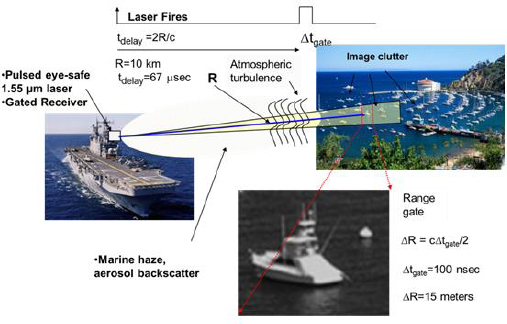
FIGURE 4-29 Illustration of the principle of range-gated imaging applied to a target in the midst of large background clutter. The use of 1.57 µm laser can significantly reduce the haze common in the marine environment. SOURCE: J. Waterman, Naval Research Laboratory.
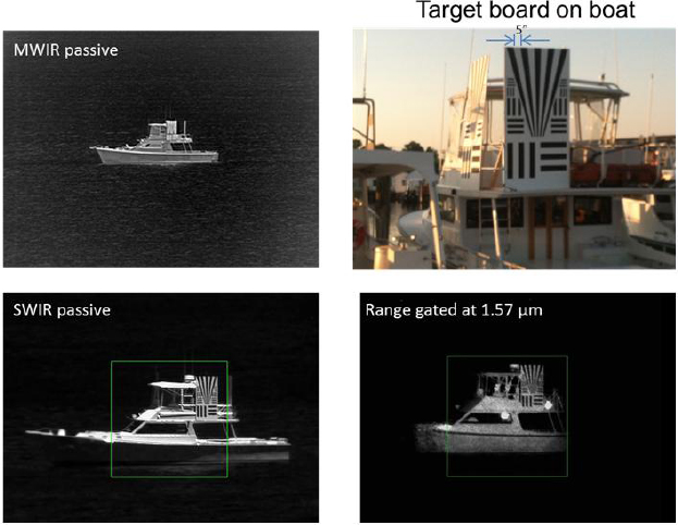
FIGURE 4-30 Passive imaging of a boat in the MWIR (top left) and SWIR (1-1.8 µm band), and range gated imaging with 1.57 µm laser all with the same FPA. Only the part of the boat that is illuminated with the laser is imaged (bottom right). The green squares in the SWIR imaging were image processed. SOURCE: DRS Technologies, Dallas, Texas.
speckle as is common due to interference effects. The image processed region within the green square drastically reduces the speckle effects, improving the image quality relative to the region outside the square.
A summary of both types of gated imaging FPAs is given in Table 4-4.
Conclusion 4-6: Geiger-mode avalanche photodiodes based on InGaAs/InP structures with single photon counting sensitivity in the 1-1.6 µm band are now available in 32 × 32, 32 × 128, and 64 × 256 pixel formats. Recently, this detector technology was extended to 2.2 µm operation using InGaAs/Gauss Type II superlative structure grown on InP. It is expected that this approach will be developed into array formats in the next few years.
Conclusion 4-7: Linear-mode avalanche photodiodes based on InGaAs/InP with single-photon counting sensitivity are available in pixel formats as large as 128 × 128 for wavelengths ≤1.6 µm. HgCdTe-based APDs with photon counting sensitivities in this wavelength band have been demonstrated in pixel formats up to 256 × 256. HgCdTe APD arrays with sensitivity from the visible to the midwave infrared (MWIR) wavelengths of 5 µm have been developed that are capable of real time 2-D and 3-D imaging. The latter arrays enable passive MWIR, passive SWIR, and active 2-D SWIR, all from the same 640 × 480 pixel format imaging array.
TABLE 4-4 Performance Characteristics of 2-D Gated Imaging IR Arrays
| Array Technology | FPA Format and Pitch (µm) | Frame Rate (Hz) | Gate Width (ns) | ROIC Noise and Operating Temperature | Spectral Range and QE | Comments |
| Intevaca, b InGaAs/InP TE EBCMOS |
640 × 480, | <30 | ≥70 ns | ~1 e- per pixel/ μsec at 20°C; | 0.95 to 1.65 μm | Gated 2-D, in production; NEPh=9 photons |
| 13.4 µm | ||||||
| -40 to +20°C | QE≥ 20% at 1.55 μm | |||||
| SELEXc HgCdTe APD | 320 × 256, 24 µm | |||||
| CEA/Letid | 320 × 240, 30 µm | 1,500 | ≤1 µs | 3-4 e- normalized with detector gain of 10; ≤200 K | 0.2–3.0 μm | Gated 2-D, 3-D SW |
| HgCdTe APD | QE > 50% | |||||
| DRSe | 640 × 480 | <120 Hz | ≥25 ns | 1-2 e- normalized with detector gain of 70; 80 K | 0.5-4.5 μm | FPA capable of passive MW, SW and gated SW; Median NEPh~2 photons |
| HgCdTe APD | 25 µm | QE >50% | ||||
a See http://www.intevac.com/intevacphotonics; LIVAR® M506.
b S. Demiguel, 2009, Proc. of SPIE 7298: 729836.
c I. Baker et al., 2008, Proc. of SPIE 6940: 69402L.
d J. Rothman, et al., 2012, J. Electronic Materials 41: 2928.
e P. Mitra DRS Technologies, Dallas, Tex.
SOURCE: P. Mitra, DRS Technologies, Dallas, Tex.
Conclusion 4-8: In the next few years it is expected both Geiger and linear-mode avalanche photodiode technologies will continue to develop to similar array sizes with comparable sensitivity. As the formats grow the pixel pitch will need to shrink to keep the size of the collection optics practical and from growing unreasonably large. Reducing the pixel pitch to sizes comparable to those being developed for passive imaging arrays will be a challenge for the ROIC technology, much more so than for the detectors. The sensitivity of linear-mode APDs is improving and is approaching that of GM-APDs.
Conclusion 4-9: The most difficult challenge for active sensing detectors going forward is the read out integrated circuit technology, regardless of which detector technology is used. While significant advances have been made in recent years, getting the signal out at high data rates, particularly for large-format arrays, remains a challenge and needs to be prioritized for future development. It is also an important area to watch in monitoring foreign developments.
Conclusion 4-10: For polarization sensing active imaging and digital holography (spatial heterodyne), a wide variety of formats is now available with standard detector technologies based on InGaAs, InSb, or HgCdTe all the way to 2K × 2K pixels. It is expected that these arrays will grow into larger formats and with pixel pitches of 5 µm or less. HgCdTe arrays with LWIR and MWIR cutoffs and response extending into the near IR have been demonstrated in 1,280 × 780, 5 µm pitch pixel format.
REMOTE ULTRA-LOW-LIGHT IMAGING
The imaging detector arrays discussed thus far are arrays of individual detectors the sensitivities of which range from many photons per pulse (e.g., “conventional” flash) to single photons (e.g., GMAPDs). In such array detectors, each pixel performs a timing measurement, and position information is derived from which detector fires. The Remote Ultra-Low Light Level Imaging (RULLI)98 detector, on the other hand, is a single large-area position-sensitive detector and is sensitive at the level of a single photon over the entire area.
Originally developed for ultra-low light passive imaging (e.g., moonless nights99), the operating principle of RULLI (below) is inherently well-suited for active 3-D imaging as well, so long as dynamic range constraints are recognized and dealt with. A single photon incident upon a photocathode produces a single electron, which is accelerated to a microchannel plate stack that provides a gain of about 107. This macroscopic pulse of charge (localized in both time and space) then passes through a planar crossed delay line, as in Figure 4-31. This produces four current pulses that then propagate in both directions along both of the crossed serpentine delay line wires. By measuring the difference in delay time for the arrival of each current pulse at the ends of the delay lines, the X-Y position of the incident electron cloud can be localized, and by measuring the arrival time with respect to the outgoing laser pulse, a time-of-flight range measurement is performed.
Thus the key technological components of a RULLI detector are the photocathode, the microchannel plate stack, the crossed delay line, and the electronics. Figure 4-32 shows the RULLI crossed delay line and assembled sensor head for the Nocturnal Camera (NCam) imaging camera built by Los Alamos National Laboratory. The active area has a 25 mm diameter and an effective number of resolution elements of 500 × 500, resolving the position of the photon arrival with a full width at half maximum (FWHM) of about 80 µm. The timing accuracy for ranging is about 1 ns, and the system can detect up to 2 million counts/s. NCam operates in the visible with a quantum efficiency of 19 percent in the green. Dark noise is quite low: <100 counts/s/mm2 at 22°C and <1 count/s/mm2 at 0°C. The packaged
____________________
98 D. Thompson, 2013, “Imaging one photon at a time,” Los Alamos report number LA-UR-13-22617.
99 Under starlit conditions, a visible remote sensing system at a range of 10 km with a 1 cm aperture and 100 percent detection efficiency will detect 1 photon per second per square meter from a target of albedo 1.
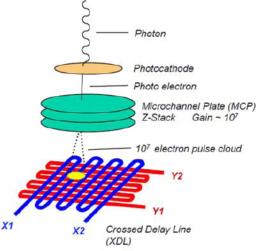
FIGURE 4-31 RULLI detector elements and concept.
SOURCE: D. Thompson, 2013, “Imaging one photon at a time,” Los Alamos Report Number LA-UR-13-22617.
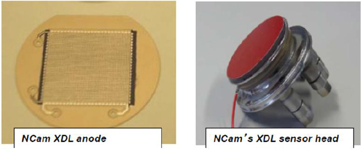
FIGURE 4-32 RULLI crossed delay line (left) and assembled sensor head (right). SOURCE: D. Thompson, 2013, “Imaging one photon at a time,” Los Alamos Report Number LA-UR-13-22617.
NCam is 5 in. × 5 in. × 13 in. and weighs 10 lb. It uses ~30 W of power from a 28 V buss or battery and is suited for airborne operation.
RULLI can operate in spectral bands other than the visible, depending on the photocathode used. Figure 4-33 shows the spectral dependence of the QE for several available photocathode materials.
FIGURE 4-33 Spectral dependence of the quantum efficiency for several available photocathode materials. SOURCE: D. Thompson, 2013, “Imaging one photon at a time,” Los Alamos Report Number LA-UR-13-22617.
FIGURE 4-34 A typical RULLI/NCam active 3-D imaging product. SOURCE: D. Thompson, 2013, “Imaging one photon at a time,” Los Alamos Report Number LA-UR-13-22617.
When operated in an active imaging mode, RULLI can produce high-quality 3-D products but operates in a rather different regime than some of the ladar systems described elsewhere in the report. Since multiple photoelectron pulses incident upon the crossed delay line can give rise to positional ambiguities, RULLI is limited to receiving only one photon per “frame.” Due to the time necessary to read out the delay line, this imposes a maximum detection rate of about 2 million photons/s. In addition, this extreme sensitivity of RULLI means that it is very sensitive to background photons, favoring nighttime moonless operation and the use of very narrow spectral filters.
Because the scene, whether in passive imaging or ladar mode, is built up one photon at a time with a maximum count rate of 1-2 MHz, the imaging time for a scene can be rather long. RULLI/NCam employs both position and attitude knowledge as well as motion compensation and registration algorithms to build the scene images as well as identify movers within a scene.
Figure 4-34 shows a typical RULLI/NCam active 3-D imaging product. This image was taken from a ground perspective (note the shadowing) using a 1 MHz pulse repetition rate from a mode-locked laser over a 10 s exposure time. The range to target in this image went from 180 m to 395 m. One limitation of RULLI is due to the high PRF required to image scenes in a reasonable measurement time. For a constant PRF, this implies an ambiguity range (determining from which transmitted pulse a given return photon came and, hence, the range to target) of Ra = c /(2·PRF). This limitation can potentially be overcome, however, with PRF modulation techniques to resolve ambiguities.
RULLI typically operates with a short laser pulse, ~100 ps. Combined with the timing precision of the crossed-delay readout, this results in a high range resolution suitable for foliage penetration (FOPEN) scenarios. Active RULLI was recently used for performing topographic lidar in the marshy riverine environment near Savannah River,100 which proved a very powerful technique compared with manpower-intensive GPS surveying and commercial airborne lidar (which typically operate with longer pulses not well suited to the marsh-grass environment.)
The low-count-rate limitation of the crossed-delay-line RULLI design can be mitigated by parallelizing the readout using an array of microstrips rather than a serpentine delay line. This is the concept behind RULLI-XS, which is being developed jointly by LANL and the University of California at Berkeley. Figure 4-35 shows the design concept, which has a goal of 108 photon counts per second over a megapixel array with <1 ns timing resolution.
FIGURE 4-35 Design concept for RULLI-XS with parallelized readout to overcome count-rate limitations.
SOURCE: D. Thompson, 2013, “Imaging one photon at a time,” Los Alamos Report Number LA-UR-13-22617.
____________________
100 D. Thompson, 2013, Imaging One Photon at a Time, Los Alamos Report Number LA-UR-13-22617.
FIGURE 4-36 Graphene’s honeycomb lattice of carbon atoms. SOURCE: By AlexanderAlUS (Own work) [CC-BY-SA-3.0 (http://creativecommons.org/licenses/by-sa/3.0) or GFDL (http://www.gnu.org/copyleft/fdl.html)], via Wikimedia Commons. Available at http://en.wikipedia.org/wiki/Graphene.
The electronic properties of graphene, one or more layers of a 2-D lattice of carbon atoms (Figure 4-36), are stimulating interesting research that may lead to important applications.101 The field is burgeoning worldwide and results suggest graphene will have an important impact on active electro-optic systems.
The electronic band structure of a single layer of graphene is simple and was analytically calculated as early as 1947.102 Because of its structural simplicity and unusual theoretical electronic properties, single layers of carbon were the basis for many early theoretical studies but the material was presumed not to exist in the laboratory.103 In defiance of its presumed nonexistence, about a decade ago surprisingly robust single-atomic-layer graphene samples became available in the laboratory. Soon the unusual properties began to be published, stimulating an expanding interest in graphene.104 The Nobel prize in physics for 2010 was awarded to Andre Geim and Konstantin Novoselov at the University of Manchester for experiments on graphene. In 2013, graphene researchers from Sweden’s Chalmers University, led by Prof. Jari Kinaret, secured an unprecedented € 1 billion105 from the European Union.106
____________________
101 A.K. Geim and K.S. Novoselov, 2007, “The rise of graphene,” Nature Materials 6: 183.
102 P.R Wallace, 1947, “The band structure of graphite,” Physical Review 71: 622.
103 More than 70 years ago, Landau and Peierls showed that 2-D crystals were thermodynamically unstable and could not exist. R.E. Peierls, 1935, “Quelquesproprietestypiques des corpses solides,” Ann. I.H. Poincare 5:177, and L.D. Landau, 1937, “Zurtheorie der phasenumwandlungen II,” Phys. Z. Sowjetunion 11: 26.
104 K.S. Novoselov et al., 2004, “Electric field effect in atomically thin carbon films” Science 306: 666.
105 The Graphene Flagship will coordinate over 125 academic and industrial research groups in 17 European countries. Initial projects will be funded with $72 million for 30-months in addition to 20-to-30 additional targeted projects that will be announced.
106 See http://europa.eu/rapid/press-release_IP-13-54_en.htm and http://www.eetimes.com/design/medicaldesign/4405947/EU-funds-research-on-graphene-brain-like-chips.
FIGURE 4-37 For a single layer of graphene the Fermi energy EF changes with gate voltage Vg; positive Vg induce electrons and negative Vg induce holes. The carrier concentrations is n = αVg, where the coefficient α ≈ 7.2 × 10¹⁰/cm2/V for field-effect devices with a 300 nm SiO2 layer used as a dielectric. The rapid decrease in resistivity ñ as charge carriers are added indicates their high mobility and does not noticeably change with increasing temperature to 300 K. SOURCE: Reprinted by permission from Macmillan Publishers Ltd: Nature Materials. A. K. Geim and K. S. Novoselov, 2007, “The rise of graphene,” Nature Materials 6: 183, copyright 2013.
The electronic properties of a single layer of graphene derive from its conical symmetric energy bands, which produce a zero bandgap (Figure 4-37), making it a semimetal. The curve of energy versus wave vector k at low energy is linear, and that could lead to infinite charge mobility; in practice, however, the mobility is limited by impurity scattering or other defects. The symmetric valence and conduction band structure makes the electron and hole mobility equal, an unusual property.
Perhaps uniquely there is an electric field ambipolar effect whereby the Fermi level changes and charges carriers tune between electrons and holes as seen in Figure 4-37. Also, the charge mobility shows surprisingly little change with temperature, with measured mobilities that exceed 15,000 cm2/V/s and with predicted mobilities being an order of magnitude higher, likely exceeding that of semiconductors.
Additional discoveries show that graphene band structure also changes107 with the following:
• Number of atomic layers of graphene,
• Details of the layer’s edge boundaries, and
• Addition of dopants or defects.
Other unusual properties are extreme physical flexibility, a very wide photon absorption spectrum (from ultraviolet to multiple terahertz) and fast photo-induced carriers (subnanosecond response time.)
____________________
107 See http://en.wikipedia.org/wiki/Graphene. The site shows an informative display of graphene band structure as a function of ribbon size and edge type. The zigzag edge structure is metallic while the “arm-chair” orientation can be semiconducting or metallic depending on the details of the edge and ribbon size.
Not all graphene properties are optimal. The band structure yields a constant value for the conductance and optical absorption over a wide spectral range, from visible to infrared.108,109 The resultant probability of a photon absorption in a single layer of graphene is about 2.3 percent.112,110 For high quantum efficiency detectors, multiple layers of graphene are needed.
The optoelectronic properties of graphene are a basis for a variety of photonic and electronic applications,111 including fast, wideband photo detectors,112 optical modulators,113 and fast lasers.114 A brief discussion of detector-related discoveries and applications follows.
Graphene Detectors
Many have recognized that graphene could make extremely wide-spectrum, highly sensitive, lownoise detectors at ambient-temperature. In 2012, Japanese, Russian, and U.S. researchers calculated the responsivity of dark-current-limited graphene photodiodes from the far IR to terahertz frequencies.115 The researchers concluded that if multiple layers of graphene were used, the resultant detectors would have high QE and relatively low rates of thermo-generation—that is, the dark current and associated noise would be small. Because graphene-based detectors can exhibit high responsivity and detectivity at elevated temperatures in a wide radiation spectrum, the researchers say they can substantially surpass the performance of other detectors116.
The benefits of graphene detectors are internationally appreciated. In June 2012 Iranian researchers published a theoretical analysis of an IR photodetector based on multiple layers of armchair-edge-boundary graphene nanoribbons (A-GNR) with a PIN structure117 (Figure 4-38).
The goal was to extend the spectral capability and reduce the cost of HgCdTe and InSb photodetectors and imagers.
The Iranian researchers realized that armchair-edge graphene nanoribbons are semiconductors and that the electronically variable energy gap can be tuned from the visible through IR to THz. The study included three designs of detectors. They used the single-electron tight binding model to calculate the band structure and then derived the quantum efficiency, the temperature-dependent optical responsivity, and the variation of these properties with nanoribbon width and number of layers. They conclude A-GNRs have energy gaps in the IR range of electromagnetic spectrum and should be good IR photodetectors.
____________________
108 A. Kuzmenko, E. Heumen, F. Carbone, and D. der Marel, 2008, “Universal optical conductance of graphite,” Physical Review Letters 100.
109 T. Stauber, N. Peres, and A. Geim, 2008, “Optical conductivity of graphene in the visible region of the spectrum,” Physical Review B 78.
110 R.R. Nair et al, 2008,” Fine structure constant defines visual transparency of graphene,” Science 320:1308.
111 F. Bonaccorso et al., 2010, “Graphene Photonics and Optoelectronics,” Nature Photon. 4: 611.
112 F. Xia et al., 2009, “Ultrafast graphenephotodetector,” Nature Nanotech. 4: 839.
113 Liu et al., 2011, “A graphene-based broadband optical modulator,” Nature 474: 64.
114 A.A. Lagatsky et al., 2013, “2µm solid-state laser mode-locked by single-layer graphene” Appl. Phys. Lett. 102: 013113.
115 V. Ryzhii, N. Ryabova, M. Ryzhii, N.V. Baryshnikov, V.E. Karasik V. Mitin, and T. Otsuji, 2012, “Terahertz and infrared photodetectors based on multiple graphene layer and nanoribbon structures,” Opto-Electron Review 20(1): 15.
116 A. K.Geim and K. S.Novoselov, 2007, “The Rise of Graphene”Nature Materials 6(3).
117 E. Ahmadi, A. Asgri, and K. Ahmadiniar, 2012, “The optical responsibility in IR-photodetectors based on armchair grapheme nanoribbons with PIN structure,” Superlattices and Microstructures, 52: 605.
FIGURE 4-38 The schematic views of the A-GNR-based IR photodetector with electrically induced PIN junction. SOURCE: E. Ahmadi, A. Asgari, and K. Ahmadiniar, 2012, “The optical responsivity in IR-photodetector based on armchair graphene nanoribbons with p—i–n structure,” Superlattices and Microstructures 52: 605, with permission from Elsevier.
Experimental verification of the broadband absorption and greatly improved sensitivity of a graphene quantum dot (GQD) enhanced detector is reported by Chinese researchers.118,119 They report high photoresponsivity from monolayer graphene photodetectors with GQDs. The high photoresponsivity is partially attributed to internal gain of four times, called multi-excitation generation of carriers. This mechanism has been predicted theoretically120 but has never been reported experimentally. It is caused by impact ionization, sometimes called inverse Auger recombination. The report includes a nearly simultaneous citation of the publication of another observation that bolsters the researchers’ explanation and observations of gain in graphene.121 They observed photoresponsivity about three orders of magnitude higher than that reported in the previous literature. In addition to utilizing gain, the increased performance is enhanced by the introduction of electron trapping centers and by optimizing a bandgap through band structure engineering.
The fabrication steps of the detector are relatively simple, as shown in Figure 4-39.
When tested over a large spectral range, there is broadband response shown from the visible (VIS) (532 nm), near-infrared (NIR) (1.47 µm) and mid-infrared (MIR) (~10 µm) ranges with photoresponses of: ~1.25 AW-1, 0.2 AW-1 and 0.4 AW-1 in the visible, NIR, and MIR ranges, respectively.
A major limitation of the detector is slow speed, as seen in Figure 4-39.
____________________
118 They have also filed for a patent through the university’s Nanyang Innovation and Enterprise Office.
119 Y. Zhang, T. Liu, B. Meng, X. Li, G. Liang, X. Hu, and Q.J. Wang, 2013, “Broadband high photo response from pure monolayer grapheme photodetector,” Nature Communications 4:1811.
120 T. Winzer, A. Knorr, and E. Malic, 2010, “Carrier multiplication in graphene.” Nano. Lett. 10: 4839.
121 K.J. Tielrooij et al., 2013, “Photoexcitation cascade and multiple hot-carrier generation in grapheme,” Nat. Phys. 9: 248.
FIGURE 4-39 Fabrication of broadband graphene experimental detector: (a) a monolayer of graphene is placed on a SiO2/Si substrate, (b) source and drain contacts are deposited, making a field effect transistor, (c) a Ti sacrificial layer is deposited for selective removal, and (d) depending on the Ti layer thickness, wet etching produces variable size regions of graphene quantum dots (GQDs). SOURCE: Reprinted by permission from Macmillan Publishers Ltd: Nature Communications. Zhang, T. Liu, B. Meng, X. Li, G. Liang, X. Hu, and Q. Jie Wang, 2013, “Broadband high photoresponse from pure monolayer graphene photodetector,” Nature Communications 4:1811, copyright 2013.
FIGURE 4-40 The slow response of a graphene dot detector to NIR light at 1.47 µm. Note the timescale is hundreds of seconds. SOURCE: Reprinted by permission from Macmillan Publishers Ltd: Nature Communications. Zhang, T. Liu, B. Meng, X. Li, G. Liang, X. Hu, and Q. Jie Wang, 2013, “Broadband high photoresponse from pure monolayer graphene photodetector,” Nature Communications 4:1811, copyright 2013.
The slow response is attributed to traps, and there are multiple ways to reduce trap times and densities. It is well know that the boundary edges of graphene can change its character from semiconductor to metallic and even introduce defects. To better define the edge boundaries of a graphene dot Yongzhe Zhang et al. suggest an electron beam, a He ion beam, and focused ion lithography that should make more precise edges and reduce disturbances in other parts of the graphene dot. The report concludes the detectors are relatively simple to fabricate, and with defect engineering the performance will continue to improve.
Graphene detectors working in the terahertz range are also reported by Italian, French, and English researchers.122 They measured a target at room temperature with a bilayer-graphene-based FET at Vg = 3. The detector was mounted on aX-Y translation stage having a spatial resolution of 0.5 µm. The THz image consists of 200 × 550 scanned points, collected by raster scanning the object in the beam focus, with an integration time of 20 ms/point. The experimental setup and results are seen in Figure 4-40.
Implications
Although graphene is an immature material technology, its potential for applications such as advanced lidar is significant. Imaging in all bands from visible to terahertz wavelengths with graphene detectors is possible, and several detector concepts are under intense development. Graphene-based, electronically-tuned, wide-spectrum imaging arrays operating at ambient temperature are possible future lidar system enablers.
Graphene edge boundaries (zigzag or arm chair) control its metallic and semiconductor properties but the boundaries require atomic accuracy and precision. Electron and ion beams are not now accurate and precise enough to make the desired boundaries because of collateral damage.
Conclusion 4-11: Electron beam processing is an important tool used in commercial semiconductor device production, but further advances will be required to develop the capability to make atomically correct graphene edge boundaries. Such techniques may be developed in the next 10-20 years, and if they are, the impact would be large.
Conclusion 4-12: Development of a scalable graphene detector array concept with appropriate fabrication tools is a noteworthy indicator that the graphene will enable new detector systems. Experimental single detectors are being theoretically explored and experimentally demonstrated for a variety of wavelengths. Advanced imaging systems likely require arrays of detectors. These arrays could be developed in the next 5-10 years and if this happens, they would have a large impact.
Conclusion 4-13: The United States has no significant lead in graphene research and development projects, and Europe has committed to the largest known graphene research and development program. Knowledge of the potential for greatly improved IR detectors and other applications is driving R&D on graphene worldwide.
QUANTUM DOT INFRARED DETECTORS
Quantum dots (QDs) are small particles with sizes on the border between chemical molecules and bulk materials. Like atoms or molecules, they have discrete electronic spectra, and like bulk materials, there are valence and conduction bands with gaps in between. In 1996, a theorist proposed to enhance IR
____________________
122 L. Vicarelli et al., 2012, “Graphene field effect transistors as room-temperature terahertz detectors,” Nature Mater. 11: 865.
detector performance by use of small 3-D embedded nanoparticles called quantum dots.123 The electronic structure of a QD is modified compared with bulk materials due the relatively large surface boundaries and low volume, and the consequently confined size of electronic excitations, called excitons, within the dot. Excitons are bound electrons and holes. They are quasi-particles because the pair has less energy than the individual constituents, making the bound pair behave like a single particle. The average relative distance between an exciton’s hole and its electron is called the exciton Bohr radius.
When the size of this hydrogen-like atom arrangement is limited by the dot volume, quantum confinement is produced. QDs are in the weak confinement if their effective radii are the size of the unconfined exciton Bohr radius or larger and in the strong confinement if their radii are smaller. If the QD is dominated by quantum confinement, typically at sizes less than 10 nm, the electronic and optical properties are highly tunable. The electronic properties of QDs have multiple degrees of freedom in addition to size such as the shape and distribution of the dots; these degrees of freedom include material composition, including dopants, and the nature of the surrounding matrix. QDs add to the topological quantum confinement options, which include zero-dimensional (a point), 1-D quantum wells (a line), 2-D quantum wires (a plane) and 3-D dots (a solid). Over the mid- and long-wavelength IR bands, QDs have predicted absorption coefficient of 104/cm; low dark current; spectral tunability by size, shape, composition, and surrounding matrix; and long photo carrier lifetimes.124 The QD geometry produces a large density of states near the conduction bandedge, creating the large absorption coefficient and temperature independent carrier distributions. The 3-D quantum confinement suppresses low-energy thermal carriers, reducing dark current compared to that in bulk material. The effective carrier lifetime is extended by a phonon bottleneck caused when the bands of QDs do not match the phonon spectrum, and the long carrier lifetime should aid collection and increase detector efficiency.125 Finally, unlike quantum wells, QDs absorb normal incident light because the geometry relaxes the polarization photon selection rules. There are claims that quantum dot infrared photodetectors (QDIPs) will outperform HgCdTe, InAs, and quantum well detectors because they are based on mature growth technologies and the low dark currents allow high temperature operation.126 These claims have not been substantiated, but there is serious, multifaceted research and new detector designs are attempting to achieve the promise.
When an IR photon is absorbed by a QD, two types of electronic transitions occur. The first type is called bound to bound, where the ground state carrier goes to an excited state confined within the QD. The second is a bound to continuum, where the ground state carrier is excited directly into a state within the surrounding matrix of the QD. To be collected, the bound to bound excited carrier must escape the QD by thermionic emission or tunneling. Once the excited carriers are out of the QD, they must then drift or be accelerated to a collection contact. During the collection process, some carriers may be captured by another QD or the same original one. These effects slow the response time, and some carriers are lost as their energy degrades from multiple interactions. It is desirable to keep QDs close to collection contacts, however to prevent strain and maintain high absorption, QDIPs require thin heterogeneous stacks of 30 or more QD active regions separated by strain-reducing matrix materials. The photocurrent must transport the entire stack to produce a signal. An example structure that attempts to optimize all the QDIP requirements is shown in Figure 4-42.
____________________
123 V. Ryzhii, 1996, “The theory of quantum-dot infrared phototransistors,” Semiconductor Science and Technology 11: 759.
124 H. Jiang and J. Singh, 1998, “Self-assembled semiconductor structures: electronic and optoelectronic properties,” IEEE J. Quantum Electron. 34(7): 1188.
125 There is controversy about the importance of phonon bottlenecks.
126 C.F. de Souza, A. Alizadeh, S. Nair, I. Saveliev, M. Blumin, H.E. Ruda, D.C. Hays, V.H. Watkins, and K.R. Conway, 2010, “Mechanism of IR photoresponse in nanopatterned InAs/GaAs quantum dot PIN photodiodes,” IEEE Journal Of Quantum Electronics, 46(5).
FIGURE 4-41 (a) Laboratory apparatus, (b) photo of a coffee-capsule box target, (c) 0.3 GHz transmission mode image of target, and (d) 0.3 GHz transmission mode image of a leaf measured under the same experimental conditions. SOURCE: Reprinted by permission from Macmillan Publishers Ltd: Nature Communications. Y. Zhang, T. Liu, B. Meng, X. Li, G. Liang, X. Hu, and Q.J. Wang, 2013, “Broadband high photoresponse from pure monolayer graphene photodetector,” Nature Communications 4:1811, copyright 2013.
FIGURE 4-42 A 30-stack pixel element of a mid- and long-wavelength IR quantum dot in the well (DWELL) focal plane array. The design includes quantum wells that add quantum confinement to further reduce dark current. The dark current improvements have not yet been realized since reported DWELL arrays operate at 80 K. SOURCE: Copyright 2011 IEEE. Reprinted, with permission, from B.S. Paskaleva, W.-Y. Jang, S.C. Bender, Y.D. Sharma, S. Krishna, and M.M. Hayat, 2011, “Multispectral classification with bias-tunable quantum dots-in-a-well focal plane arrays,” IEEE Sensors Journal 11(6), June.
Research Directions
The lack of theoretical performance from QDIPs could be related to QD growth mechanisms. The standard QD material is grown by MBE and materials such as InAs/GaAs. MBE produces QDs with lateral sizes from 15 to 25 nm, heights from 5 to 8 nm, and pyramidal shape. The density of InAs/GaAs QDs range from 109-1011 cm-2. Dopants are added to produce two electrons in the filled ground state of the QD. For higher dopant densities, the dark current increases since the additional electrons occupy excited-state energy levels. These excited-state electrons can more easily contribute to the noise in the device by activating thermionic emission or field-assisted tunneling. For lower dopant densities, the absorption efficiency decreases since there are fewer electrons in the QD ground state available for photoexcitation. This trade-off is difficult to circumvent.
The nonuniformity of QDs grown by strained-layer epitaxy also limits realization of the predicted advantages of QDIPs. Materials improvements such as control of dopants, bandgap engineering such as DWELL, and the incorporation of resonant photonic structures are promising developments aimed at overcoming these limitations. In addition, fundamentally different QD material systems, such as colloidal QDs embedded in conducting polymers, could achieve inexpensive, room-temperature IR photodetectors. There are also proposals to add avalanche gain to QDIPs.
A recent innovative proposal suggests that photo avalanche gain can be added to QDIPs to achieve single-photon sensitivity.127
Calculations for this detector design predict that the self-quenching time is 150 ps; the dark current may allow operation at between 100 and 160 K and a detector efficiency of 8 percent at 6 µm.
Conclusion 4-14: Quantum dot infrared photodetectors promise to become an important technology in the field of infrared photodetection, particularly for the high operating temperature, high speed, multispectral imaging needs of the military and other sophisticated applications such as laser radar. Much research and development is needed to realize this promise.
Optical antennas can be thought of as extensions of microwave antennas into optical wavelengths. One definition of an optical antenna is this: “a device designed to efficiently convert free-propagating optical radiation to localized energy, and vice versa.”128,129 The approach is to use nanotechnology and plasmonics to create optical analogs of microwave antennas for detecting weak signals. Optical antennas exploit the unique properties of metal nanostructures, which behave as strongly coupled plasmas at optical frequencies and can focus electromagnetic waves into localized areas. To date, several reports have demonstrated surface plasmon-enhanced photodetectors using dipole antennas, metal hole arrays, and bulls-eye gratings. Figure 4-43 shows an example.
____________________
127 M. Zavvari and V. Ahmadi, 2013, “Quantum-dot-based mid-IR single-photon detector with self-quenching and self recovering operation,” IEEE Electron Device Letters 34(6): 783.
128 P. Bharadwaj, B. Deutsch, and L. Novotny, 2009, “Optical antennas,” Adv. Optics Photonics 1: 438.
129 This is relatively new usage, in that in addition to being the receiving or transmitting element, it includes focusing light to be detected and presumably to assist in transmission. On p. 101 of an earlier NRC report Seeing Photons, an optical antennas is defined as a transduction device that is used to transmit or receive electromagnetic radiation. This is more restrictive usage, more like the definition used in the RF regime. Seeing Photons provides a discussion of optical antennas in the narrower definition. Because of the promise associated with focusing optical radiation, the expanded definition has been used lately, so additional discussion beyond that in Seeing Photons is required here.
FIGURE 4-43 An example of optical antennas that enhance optical electric fields to a localized area for enhanced detection capability. Such tiny structures can be combined into sparse detector arrays. The scale in (a) is 2 µm. SOURCE: P. Bharadwaj, B. Deutch, and L. Novotny, 2009, “Optical antennas,” Advances in Optics and Photonics 1: 438.
The antenna, using the definition above, can increase the optical energy density that falls on a photodetector, thereby increasing its efficiency. For a detector small compared with the wavelength λ, the received power is increased by the enhancement factor of the antenna (ratio of the intensity at the detector with and without the antenna). The expectation is that, as a result of an optical antenna, the optical intensity at the detector can be two to three orders of magnitude higher than the incident intensity. As was reported from Stanford, a half-wave Hertz dipole antenna (similar to those used for radio waves) of length ~ 380 nm for use at near-infrared wavelength of ~1.3 µm, was used to concentrate radiation into a nanometer-scale germanium photodetector. Antenna enhancement was demonstrated through a polarization contrast ratio of 20 in the photocurrent generated in the germanium element, which had an active volume of 0.00072 µm3, two orders of magnitude smaller than previously demonstrated.130
While not as sensitive as other technologies, these detector arrays have the advantage of operating at room temperature and are valuable in the long-wave infrared (7-14 µm wavelengths). Much research on developing improved designs is under way. Of the many designs, only two more will be mentioned here. One is the promising use of surface plasmon antenna structures to concentrate light below the diffraction limit. Researchers at the University of California Los Angeles used nanopillars as absorbers for antennas in photodetector array applications.131 According to Senanayake et al. “their small volume and high material quality results in a lower leakage current and junction capacitance, giving better noise performance and higher-speed operation than typical planar photodetectors… however, there is typically a tradeoff between the size of the absorbing volume and the quantum efficiency of the photodetector when the thickness of the semiconductor junction is reduced below the optical absorption length”132. Their solution takes advantage of antennas to boost the signal. Senanayake et al. determined that there was an
____________________
130 L. Tang, S.E. Kocabas, S. Latif, A.K. Okyay, D.-S. Ly-Gagno, K.C. Saraswat, and D.A.B. Miller, 2008, “Nanometre-scale germanium photodetector enhanced by a near-infrared dipole antenna,” Nature Photonics 2: 226.
131 P. Senanayake, C.-H. Hung, J. Shapiro, A. Scofield, A. Lin, B.S. Williams, and D.L. Huffaker, 2012, “3D Nanopillar optical antenna photodetectors,” Optics Express 20(23): 25489.
132 Ibid.
18-foldenhancement of electric field intensity near the partial gold shell on the nanopillar sidewalls. A pitch of 580 nm gave resonances within the absorption spectrum of the In0.35Ga0.65As material. Their experimental data indicated that absorption was enhanced by of a factor of 3 due to the localized surface plasmon supported by the metal cap.
In another demonstration of the ability of optical antennas to assist with measuring small optical signals, other Stanford researchers redesigned a metal-semiconductor-metal (MSM) photodetector consisting of a Ge nanowire so that its two metallic contacts served as optical antennas capable of concentrating light in the nanowire by a factor of 1.7.133 The reported advantages of MSM photodetectors are high speed and low noise. The optical antenna was also designed to control the detector’s polarization-dependent response.
Research in “optical antennas is currently driven by the need for high field enhancement, strong field localization, and large absorption cross sections in near-field applications.”134 This includes antennas for high-resolution microscopy and spectroscopy. Other suggested applications are increased efficiency in photovoltaics. The antenna can also be used as a light emitter, typically emitting controlled radiation from very small dimensions and used locally. In these ways optical antennas can make photonic processes more efficient and increase the specificity of gathered information.135 Optical antenna arrays have not yet been demonstrated for long-range sensing, but this may happen in the future.
Some studies have predicted that intensity enhancements of 104-106 are feasible. This means that optical antennas might reduce the area of discrete absorbers by 4-6 orders of magnitude without sacrificing any loss of absorption. One potential application might be mid-infrared sparse sampling detector arrays that would work at room temperature. The suggested increase of 106 in signal could compete with Geiger-mode or other avalanche detectors.
Room-temperature microbolometer detector arrays have been developed for room-temperature sensitivity in the 7-4 µm wavelength range by BAE Systems, Lexington, Massachusetts, DRS Technologies, Dallas, Texas, Raytheon Vision Systems, Goleta, California, and others. In a commercial focal-plane array of 320 × 240 or 640 × 480 pixels, each microbolometer contains a thermally sensitive microbridge of vanadium oxide surrounded by silicon nitride.136 The microbolometers are spaced at a 46 or 17 µm pitch respectively, and have a reported electrical NEP of 0.9 pW/Hz1/2.
Researchers have integrated microbolometer arrays with optical antennas in order to increase the sensitivity. LWIR uncooled microbolometer detector arrays were reported in Russia in 2009.137 The design was similar to the BAE arrays, but integrated antennas with the uncooled microbridge high-resistance microbolometers. The array was also 320 × 240 elements, with a reported threshold power of 160 pW/pixel in the 8-14 µm range and a response time of 12-16 ms. Their NEP appears to be 1.2 nW/Hz1/2. This microbolometer array was also tested at terahertz frequencies. They measured a threshold power at 2.3 THz of 33 nW/pixel in a 160 × 120 format at a rate of 90 frames/s. This appears to be a NEP of 3.5 nW/Hz1/2.
Recently, a sensitive camera integrating an array of THz optimized antenna-coupled microbolometers was demonstrated in France to spatially image a terahertz pulse.138 A highly sensitive
____________________
133 P. Fan, K.C.Y. Huang, L. Cao, and M.L. Brongersma, 2013, “Redesigning photodetector electrodes as an optical antenna,” Nano. Lett. 13: 392.
134 L. Novotny, 2009, “Optical Antennas: A New Technology That Can Enhance Light-Matter Interactions,” The Bridge 39:4.
135 Ibid.
136 N. Butler, R. Blackwell, R. Murphy, R. Silva, and C. Marshall, 1995, “Dual use, low cost microbolometer imaging system,” in Infrared Technology XXI, Proc. SPIE 2552: 583.
137 M.A. Dem’yanenko et al., 2009, “Microbolometer detector arrays for the infrared and terahertz ranges,” J. Opt. Technol. 76(12): 739.
138 J. Oden, J. Meilhan, J. Lalanne-Dera, J.-F. Roux, F. Garet, J.-L. Coutaz, and F. Simoens, 2013, “Imaging of broadband terahertz beams using an array of antenna-coupled microbolometers operating at room temperature,” Optics Express 21(4): 4817.
suspended membrane microbridge was developed at CEA-Leti, along with a terahertz antenna design based on crossed antennas and a resonant cavity, as shown in Figure 4-44. Arrays of 320 × 240 microbolometers were collectively processed at video frame rates above CMOS wafers by integration with a CEA-Leti designed application-specific integrated circuit. The estimated average power exciting a pixel was 0.26 nW, measured at 25 images/s. Their NEP appears to be 260/(25)1/2pW/Hz1/2 = 52 pW/(Hz)1/2, showing how well-designed antennas can increase the sensitivity compared to the Russian results. None appear yet to match the sensitivity of the BAE Systems detector.
Conclusion 4-15: None of the current antenna-coupled detectors is ready to be used in EO sensing applications, but in the next 5-10 years they may have a role to play in room-temperature, longwave infrared detector arrays.
FIGURE 4-44 Geometry for microbridge microbolometer coupled to crossed microantenna. SOURCE: P. Bharadwaj, B. Deutsch, and L. Novotny, 2009, “Optical antennas,” Advances in Optics and Photonics 1: 438.
FIGURE 4-45 Two current optical gimbals: the Raytheon MTS-A (left) and MTS-B (right). SOURCE: http://www.raytheon.com/newsroom/technology_today/2012_i2/multispectral.html.
BEAM STEERING AND STABILIZATION
Active EO sensors need to point and stabilize the transmit beam and the receiver field of view. Gimbals are mechanically complex and expensive but can steer very accurately over wide angles. Except for obscurations, a three-axis gimbal can point in any direction. Figure 4-45 shows two current optical gimbals.
As can be seen, the mirror, which is the maximum size of the optical beam, is much smaller than the gimbal. A hole 2.5 to 3 times the size of the mirror must be cut in the vehicle on which the gimbal is mounted. Most military optical systems today use gimbal pointing. Gimbals can usually be pointed and stabilized very accurately but tend to cost hundreds of thousands of dollars.139 Some estimates of gimbal cost are as follows: pilotage gimbals, perhaps 14 in. in diameter, cost on the order $75,000 to 100,000; medium altitude mission gimbals, perhaps 17 in. in diameter, on the order of $100,000 to 125,000, and high altitude gimbals, perhaps 22 in. in diameter, on the order of $150,000 to 175,000.140
Another very popular method of pointing is a fast steering mirror (FSM). An FSM is just a flat mirror that can be moved over small angles very quickly. Figure 4-46 shows an FSM. There is a trade-off with respect to the size of an FSM. The larger the mirror the more power it will take to move it quickly. For that reason one would like FSMs to be relatively small, so one wants to place them where the optical beam is small. At the same time the final steering angle is reduced by magnification, as shown below.
![]()
where θf is the final steering angle and θ is the actual angle steered by the steering mirror. M is magnification. If the beam is very small where one has the FSM in the system and the beam has to be magnified, then the steering angle is reduced by the magnification.
FIGURE 4-46 A fast steering mirror. SOURCE: Courtesy of NASA/JPL-Caltech.
____________________
139 See http://www.churchillnavigation.com/gimbals, downloaded April 25, 2013.
140 Personal communication from Jeanette Lurier, Raytheon, July 31, 2013.
FIGURE 4-47 Early Lockheed Martin Risley prism.
SOURCE: Courtesy of Dennis J. Adams, Lockheed Martin MST.
Steering flats look just like FSMs. The only difference is they are bigger and slower. One way to drive steering flats is using galvanometers. A “galvanometer is a type of sensitive ammeter, an instrument for detecting electric current.”141 “It is an analog electromechanical transducer that produces a rotary deflection of some type of pointer in response to electric current flowing through its coil in a magnetic field.”142
Rotating polygonal mirrors have some advantages.
The only motion is simple rotation. Because the mirror has many sides, one does not have to rotate it fast to scan the angle rapidly. Of course, one can scan in only one dimension with a polygon.
Recently, Risley prisms,143 and even Risley gratings,144 have become more popular. Risley gratings are lighter and can be moved quicker but have dispersion. For narrow-band systems, Risley gratings have an advantage over Risley prisms. Figure 4-47 shows an early Lockheed Martin Risley steering stage. The OPTRA Risley prism steering stage, is an example of a commercial Risley steering device. Risley prisms work by rotating two or sometimes three steering prisms. It is possible to steer to large angles with Risleys using only rotation, a very simple motion. The OPTRA devices a linear fill factor of only a little more than 50 percent. Lockheed Martin has a Risley device with a linear fill factor of about 80 percent.145
Lockheed Martin increases the fill factor by placing the motor and much of the rotation mechanism in an area where the beam is smaller. Risley prisms have a zero crossing issue. If one tracks through zero one needs to rotate the wedges by 180 degrees. Risley gratings solve this problem by switching the rotation from one handedness to the other. One other advantage of Risley prisms is that they can be flush with the surface they are mounted in. Gimbals stick out into the wind stream but can point over very wide angles. Risley prisms are a flush, or conformal, steering approach. Of course any time one
____________________
141 See http://en.wikipedia.org/wiki/Galvanometer, Feb 24.
142 See http://en.wikipedia.org/wiki/Galvanometer, Feb 24.
143 See http://www.optra.com/images/TP-A_New_Look_at_Risley_Prisms.pdf, December 6, 2013.
144 C. Oh, J. Kim, J. Muth, S. Serati, M.J. Escuti, 2010, “High-throughput, continuous beam steering using rotating polarization gratings,” IEEE Photonics Technology Letters 22(4): 200.
145 D.J. Adams, A.F. Lindsay, B.L. Stamper, C.T. Knorr, A.P. Seibel, and M.R. Crano, “Risley Integrated Steering Module, Patent # 7898712 B2, March 12, 2011.
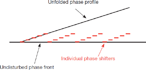
FIGURE 4-48 Modulo 2π beam steering at the design wavelength. SOURCE: Copyright 2013 IEEE. Reprinted, with permission from P.F. McManamon, P.J. Bos, M.J. Escuti, J. Heikenfeld, S. Serati, H. Xie, and E.A. Watson, 2009, “A review of phased array steering for narrowband electro-optical systems,” Proceedings of the IEEE 97(6): 1078.
steers using a steering mechanism that is flush with a flat surface there is a cosine loss in power sent to a given angle, where the cosine is taken from a perpendicular direction. This cosine loss is due to the projected area of the aperture in the direction the beam is propagated.
Many nonmechanical approaches to beam steering were reviewed in a 2009 review paper.146 A more informal discussion of was given in a magazine article a few years earlier.147 The basic physics for any phased array beam steering approach is to modulate the optical path difference (OPD), or the phase, of the outgoing or incoming wave across an aperture to steer to a given angle. In order to minimize the amount of OPD or phase modulation required, often a modulo 2π phase modulation approach is used, subtracting 2π phase whenever the imposed phase become more than 2π. For single-frequency beams, this can be done with no effect on the steering angle, but 2π phase for one carrier frequency is not the same amount of OPD as for another carrier frequency, so this makes the steering approach dispersive. The basic approach to liquid crystal beam steering is to modulate the OPD and to use modulo 2π resets to limit the amount of OPD required. Basic liquid crystal beam steering using nematic liquid crystals at room temperature has about a 10 ms switching time. Modulating OPD is the same as modulating phase at the design wavelength. If the wavelength is not identical to the design wavelength, however, the beam will steer to a different angle, and usually sidelobes are developed. Figure 4-48 shows the unfolded phase for modulo 2π beam steering. As one can see in Figure 4-48, there also can be a digitizing error if the number of steps in a profile is limited.
The angle one can steer to at high efficiency using liquid crystal beam steering is limited to small angles primarily due to fringing field effects. When the 2π reset occurs, the OPD is supposed to drop sharply in position across the aperture from the 2π phase to the zero phase at the design wavelength. Because the OPD is generated by placing a voltage across a liquid crystal cell, and fringing fields limit how fast the voltage can change, this reset is not as sharp as it should be for liquid crystal beam steering. Figure 4-49 shows the effect. The net result is that a portion of the aperture steers the beam in the wrong
____________________
146 P.F. McManamon, P.J. Bos, M.J. Escuti, J. Heikenfeld, S. Serati, H. Xie, and E.A. Watson, 2009, “A review of phased array steering for narrowband electro-optical systems,” Proceedings of the IEEE 97(6): 1078.
147 P.F. McManamon, 2006, “Agile nonmechanical beam steering,” Optics and Photonics News 17(3): 21.
FIGURE 4-49 Reset limitations due to fringing fields. SOURCE: Copyright 2013 IEEE. Reprinted, with permission from P.F. McManamon, P.J. Bos, M.J. Escuti, J. Heikenfeld, S. Serati, H. Xie, and E.A. Watson, 2009, “A review of phased array steering for narrowband electro-optical systems,” Proceedings of the IEEE 97(6): 1078.
direction, reducing efficiency, and high-efficiency steering is limited to small angles. Other efficiency losses using liquid crystal beam steering include the loss because each step is digital and also a loss due to spatial inertia in liquid crystals, which has an effect similar to the fringing field effect. Usually this second loss term is smaller than the fringing field effect, but not always.
Using the equations in McManamon et al.148 it can be seen for 98 percent steering efficiency in one direction it is possible to steer to only about 0.2 degrees for a 1.5 µm wavelength and a liquid crystal birefringence of 0.35.
There are some new options for nonmechanical beam steering.149 The basic physics of optical phased arrays are the same whether one uses a chip or uses birefringent liquid crystals to create OPD. The chip approach may not however have fringing field issues. The approach shown in the referenced paper does create OPD and does use modulo 2π beam steering. This particular chip is 64 × 64, with a pitch of 9 µm × 9 µm, making the array ~576 × 576 µm. The individual antenna radiators inside a pixel are 3.0 µm long, 2.8 µm wide. A second chip-scale optical phased array150 uses random element pitch to reduce sidelobes but is also a very small chip. Often when phased-array individual elements are larger than a wavelength, people talk about the spurious sidelobes. Another way to consider this is that the largest FWHM angle that can be steered to without significant sidelobes is limited by the size of the individual phase shifters to151:
![]()
where λ is wavelength and d is the size of the individual phase shifter. Since steering is in only one direction and a higher efficiency than 50 percent (half max) is desired, it is necessary to restrict the steering angle to about one-fourth of that value. If 3 µm is used as the size of the radiator and 1.5 µm is
____________________
148 P.F. McManamon, P.J. Bos, M.J. Escuti, J. Heikenfeld, S. Serati, H. Xie, and E.A. Watson, 2009, “A review of phased array steering for narrowband electro-optical systems,” Proceedings of the IEEE 97(6): 1078.
149 J. Sun, E. Timurdogan, A. Yaacobi, E.S. Hosseini, and M.R. Watts, 2013, “Large-scale nanophotonic phased array,” Nature 493: 195.
150 D. Kwong, A. Hosseini, Y. Zhang, and R.T. Chen, 2011, “1 × 12 unequally spaced waveguide array for actively tuned optical phased array on a silicon nanomembrane,” Applied Physics Letters 99: 051104.
151 J. Goodman, 1968, Introduction to Fourier Optics, San Francisco, Calif.: McGraw-Hill, 65.
the wavelength, steering can be done to about 1/8th radian, or about 7 degrees. In one example,152 the chip is only about 576 µm—a very small aperture. Assuming a 10 cm beam, this implies a magnification of about a factor of 174, reducing the 7 degree steering angle to 0.04 degrees. Over time the steering arrays will become larger and the individual steering elements will became smaller. Sun et al. discuss only transmitting, not receiving, which is another required growth area. It is likely that nanofabricated phased arrays will become an interesting option for steering to small angles, using magnification after steering.
Another non-mechanical option for beam steering not covered in the McManamon et al., 2009 paper is called a Steerable Electro Evanescent Optical Refraction (SEEOR) prism. This device uses liquid crystals (LCs) “as an active cladding layer in a waveguide architecture where light is confined to a high index core and the evanescent field extends into the variable-index liquid-crystal cladding,”153 This allows very large optical path delays, so for small apertures it eliminates the need for a 2π reset. Therefore, there is no fringing field issue. Also, because the liquid crystal layer is thin these devices can be relatively fast, responding in under 500 µs.154,155 In-plane steering is accomplished by changing voltage on one or more prisms filled with liquid crystals, as shown in Figure 4-50.
Out-of-plane beam steering is based on the waveguide coupler designed by at Bell Laboratories in 1971 (see Figure 4-51).156 In any waveguide, “if the cladding is too thin, light will leak out of the guided mode.”157 “In a planar slab waveguide Snell’s law gives the propagation angle of the escaping light.”158 Since it is possible to tune the effective index of the waveguide, it is therefore possible to tune the angle of the escaping light.159
This waveguide-based liquid crystal beam steering can steer over relatively wide angles rapidly, but is limited to small apertures. In-plane steering can be up to 60 degrees or more in either direction, depending on the exact geometry. Out-of-plane steering can be 15 degrees or so in either direction. The main limitation on this technique is the size of the aperture, which will be limited to ~1 cm on a side or less.
Because of angle limitations on high-efficiency liquid crystal beam steering, and aperture size limitations on both the chip-scale steering and waveguide-based LC steering, there has been an interest in wide-angle step-stare steering approaches. Two techniques were initially used for wide angle beam steering in conjunction with liquid crystal steering: holographic glass and birefringent prisms.160 From McManamon:161
____________________
152 J. Sun, E. Timurdogan, A. Yaacobi, E.S. Hosseini, and M.R. Watts, 2013, “Large-scale nanophotonic phased array,” Nature 493: 195.
153 S.R. Davis, S.D. Rommel, G. Farca, B. Luey, N. Rebolledo, S. Selwyn, M.H. Anderson, 2011, “A new photonics technology platform and its applicability for coded aperture techniques,” Proc. SPIE 8165: 81651E, Unconventional Imaging, Wavefront Sensing, and Adaptive Coded Aperture Imaging and Non-Imaging Sensor Systems.
154 S.R. Davis, S.T. Johnson, S.D. Rommel, M.H. Anderson, J. Chen, and T.-H. Chao, 2013, “New electro-optic laser scanners for small-sat to ground laser communication links,” Proc. SPIE 8739: 87390H, Sensors and Systems for Space Applications VI.
155 S.R. Davis, G. Farca, S.D. Rommel, S. Johnson, and M.H. Anderson, “Liquid crystal waveguides: New devices enabled by >1000 waves of optical phase control.” Proc. SPIE 7618: 76180E, Emerging Liquid Crystal Technologies V.
156 R. Ulrich, 1971, “Optimum excitation of optical surface waves,” Journal of the Optical Society of America 61: 1467.
157 S.R. Davis, G. Farca, S.D. Rommel, S. Johnson, M.H. Anderson, “Liquid crystal waveguides: New devices enabled by >1000 waves of optical phase control,” Proc. SPIE 7618: 76180E, Emerging Liquid Crystal Technologies V.
158 Ibid.
159 Ibid.
160 P. McManamon, 2006, "Agile Nonmechanical Beam Steering," Opt. Photon. News 17(3): 24-29.
161 Ibid.
FIGURE 4-50 Voltage-tunable liquid crystal waveguide based in-plane steering.
SOURCE: S.R. Davis, G. Farca, S.D. Rommel, S. Johnson, and M.H. Anderson; “Liquid crystal waveguides: new devices enabled by >1000 waves of optical phase control,” Proc. SPIE 7618:76180E, Emerging Liquid Crystal Technologies V.
FIGURE 4-51 Liquid crystal waveguide for out-of-plane steering. SOURCE: S.R. Davis, G. Farca, S.D. Rommel, S. Johnson, M.H. Anderson, “Liquid crystal waveguides: new devices enabled by >1000 waves of optical phase control,” Proc. SPIE 7618:76180E, Emerging Liquid Crystal Technologies V.
In the holographic glass approach, multiple holograms are angularly multiplexed in a single piece of glass. The holograms produce large angle deflections.
A liquid crystal beam steerer in front of the glass selects which hologram is addressed, resulting in the desired large angle of deflection.
Many layers of holographic glass can be used.
A second approach to wide-angle beam steering was birefringent prisms.
This technique also starts with an azimuth/elevation liquid crystal beam steerer for small-to moderate-angle beam steering.
Larger angles are reached using a set of binary birefringent prisms.
One polarization sees the prism deflecting the beam in one direction, while the other sees the prism deflecting it the other way.
More recently the most popular wide angle beam-steering approach is digital steering using polarization birefringent gratings. Fixed-angle digital versions of this steering are similar to birefringent prisms but use a set of gratings steering to fixed angles instead of using prisms. Such prisms are very efficient and very thin.162 They are based on a fundamentally different method of nonmechanical beam steering,163 in which the phase rather than the OPD is modulated. At the design wavelength this does not make any difference, but at any other wavelength there will be difference. The relatively mature approach to polarization birefringent steering uses set digital steering angles. There has been some work toward steering to adjustable angles that uses this approach, but it is a relatively immature at this time and very slow.164
Microelectromechanical systems (MEMS), lenslets, and electrowetting are alternative methods of nonmechanical beam steering.165 At this time they are not as efficient as using the polarization birefringent gratings in combination with either an FSM or a liquid spatial light modulator for small angle steering.
Ideally one would like optical phased arrays similar to RF phased arrays, where it is possible to build a transmit/receive (T/R) module that is a fraction of a wavelength in size. In an ideal world, each of those T/R modules would be able to delay phase enough to provide true time delay steering. This means that a 45-degree steering angle, with a 20 cm diameter aperture would have a phase delay of 14.1 cm, or almost 100,000 wavelengths at 1.5 µm wavelength. This is ideal, but will be very challenging. The steering system can be much simpler if each dimension is steered separately because many fewer steering elements are required. Also, of course, one would like very rapid beam steering. If chip-scale approaches to wide angle continuous beam steering are used, chips will tend to be small, requiring magnification in the system.
One of the really interesting aspect of phased arrays, whether optical or RF, is the ability to track to a very small fraction of the diffraction-limited beam width.166 In the classic 1968 paper on digital phased arrays it is shown that with modulo 2π beam steering one can adjust only one phase modulator in one phase ramp, and it has essentially the same effect as if much smaller modulators were used in every phase ramp. This means one can steer to 1/100th of a diffraction-limited spot size, or even better, using digital phased array steering technology.
Right now one can steer to large angles nonmechanically, but it requires many stages of beam steering. If the polarization birefringent grating approach to beam steering could be made variable and fast, this would be close to the grail for beam steering. If chip-scale optical phased arrays could be made with micron-class pitch and relatively large chips, this could be a viable continuous steering approach to be combined with fixed polarization birefringent gratings. Another viable continuous steering approach that can be used before beam expansion in combination with a stack of polarization birefringent gratings is the waveguide liquid crystal approach to nonmechanical steering.
____________________
162 J. Kim, C. Oh, M. J. Escuti, L. Hosting, and S. Serati, 2008, “Wide-angle nonmechanical beam steering using thin liquid crystal polarization gratings,” Proc. SPIE 7093, Adv. Wavefront Contr.: Methods, Devices, Applicat. VI.
163 S. Pancharatnam, 1955, “Achromatic combination of birefringent plates,” Proc. Indian Acad. Sci. XLI (4): 137.
164 L. Shi, P.F. McManamon, and P.J. Bos, 2008, “Liquid crystal optical phase plate with a variable in-plane gradient,” J. Appl. Phys. 104: 033109.
165 P.F. McManamon, P.J. Bos, M.J. Escuti, J. Heikenfeld, S. Serati, H. Xie, and E.A. Watson, 2009, “A review of phased array steering for narrowband electro-optical systems,” Proceedings of the IEEE 97(6): 1078.
166 B.R. Hatcher, 1968, “Granularity of phased positions in digital phased arrays,” Proceedings of the IEEE 56(11).
Pointing and stabilizing to very small angles is an expensive proposition, involving large optics. The newest methods of pointing and stabilization will be seen in the literature. Some very new nonmechanical approaches require lithographic, chip-scale processes.
Some form of beam steering and stabilization is required for active EO sensing. The issues considered here are the advantages and disadvantages of the new nonmechanical steering or other approaches.
The potential for random access, rapid steering is a significant advantage for optical-phasedarray, nonmechanical steering and stabilization approaches. The ability to stabilize very precisely is a second very important feature of optical phased array approaches that steer based on writing phases using discrete electronics. Compactness, lower cost, and much higher reliability are all other possible advantages.
The relative immaturity of many nonmechanical approaches is a disadvantage. Also, at this writing, many stages are required to obtain continuous large-angle steering. Efficiency is also still an issue, and speed is another issue with some approaches. This is a developing area.
Active EO sensors need to point both the transmitter and the receiver at the object being sensed. Since active sensors bring their own photons often it is desirable to be cued to a small region to limit required illuminator power. If the transmitted laser beam is relatively wide and high-resolution imaging is desired, then a large receiver FPA is needed. So-called flash imagers use this approach, while scanning imagers use a narrow field of view quickly scanned. Scanned imagers put more stringent requirements on beam steering and stabilization because the beam must be pointed and stabilized to within a fraction of one angle/angle pixel. Beam steering and stabilization can be achieved many ways. Often, laser sensing systems are narrowband, which improves the beam steering options because one does not have to worry about dispersion in the beam steering mechanism. One significant advantage with some non-mechanical beam steering approaches is the ability to point in random directions over the field of regard rather than having to scan through all points between the current pointing location and the desired pointing location.
Europe and the United States both make gimbals and FSMs. Risley prisms do not have a large barrier to entry. In fact, the barriers to entry for almost all the optical phased array steering approaches are relatively small. While the United States is currently ahead in the development of this technology, the lead is fragile.
Conclusion 4-16: Polarization birefringent gratings will gain an increasing share of the beam steering for active EO sensors, especially when combined with flash imaging techniques.
Conclusion 4-17: Steerable electro-evanescent optical refraction prism waveguides will be used for smaller aperture, closer range ladars and to steer the beam before beam expansion in conjunction with polarization birefringent gratings.
Detectors
Cryogenically cooled IR detectors require complementary accompanying technologies of refrigeration and thermal isolation in order to produce the sensitivities and performance parameters that are desired. When IR sensors began to move out of the laboratory and into tactical applications in the 1960s, the first sensors to do so relied on adaptations of the laboratory equipment, primarily the refrigerators and vacuum systems. As such, these initial systems were large, heavy, and power hungry, better suited to lab conditions than the rigors of tactical environments. While providing much needed capability in the field, the systems required significant levels of support.
As the capability of the systems increased and the possible applications expanded, concerted design efforts were undertaken to provide cryogenic and vacuum packaging solutions that were better
FIGURE 4-52 Evolution of cryocooler and IR detector packaging. IDCA, integrated detector/cooler assembly. SOURCE: D. Rawlings, DRS Technologies, Dallas, Texas.
suited to the tactical environments, were lighter and smaller, used less power, required less support, and offered high reliability. Figure 4-52 illustrates graphically the trend in size, weight, and power (SWaP) and reliability that has resulted from the focus of the user community and the sensor suppliers on removing the barriers to IR sensor adoption.
The first major push in SWaP reduction and reliability increase came with the development of the common module components and the forward looking infrared (FLIR) sensors in the 1970s. The concept broke the sensor down into basic building blocks and separated the cryogenic cooling function from the vacuum insulation packaging function, resulting in two components: the cryocooler and the vacuum Dewar.
Cryocoolers
The majority of cryogenic coolers for infrared sensors are based on the Stirling refrigeration cycle. This refrigeration process relies on pressure fluctuations within a reciprocating gas flow to extract energy from the refrigeration space; no liquid is produced and there is no refrigerant loop as is found in the more common commercial and consumer refrigerators. The working gas for Stirling cryocoolers is most commonly helium, used for its thermal properties. An early common module cryocooler is shown in Figure 4-53.
Cryocooler Classification
Most of the cryocoolers utilized in IR sensor systems can be classified as either rotary or linear drive.
FIGURE 4-53 Common module cryogenic cooler of 1 W.
SOURCE: DRS Technologies, Dallas, Texas.
Rotary Drive
The first of the common module cryocoolers used a rotary frameless AC motor as the primary driver of the compressor and expander pistons. A crank-slider mechanism converted the rotary motion to reciprocating piston action to provide the required pressure fluctuations. As electric motor technology has advanced, the rotary drive mechanisms have evolved and for the most parthave brushless DC motors that utilize high-performance permanent magnet materials to convert the electrical drive to rotary motion. Concurrent with the development of the high-efficiency motors, rotary-drive compressors have seen improvements in the basic compressor mechanisms to reduce wear on the compressor seals, reduce reliance on bearing lubricants, and improve overall reliability.
Linear Drive
In efforts aimed at improving cryocooler reliability for space mission applications, an additional class of cryocooler compressor was developed. These cryocoolers utilized a “linear” drive motor—either a moving magnet or moving coil approach—where the driving mechanism was directly coupled to the compressor piston. No conversion of rotary to linear motion was required. This approach allowed compressors to be designed without the crank-slider mechanisms of the rotary cooler, reducing mechanical complexity, eliminating bearings (and lubricants), and providing a straightforward path for implementation of contact-free “clearance” seals in the compressor. By producing the compressor as two moving pistons, linearly opposed and moving 180 degrees out of phase, virtually vibration-free compressors could be realized. Figure 4-54 illustrates this approach, and Figure 4-55 shows some examples.
Pulse-Tube Cryocooler
A variant of the Stirling cycle that has seen considerable development activity in recent years is the pulse-tube cryocooler. The pulse tube does away with the moving “displacer” component that is found in the standard configuration Stirling cycle cryocooler. By eliminating this moving element, the pulse tube offers reduced mechanical complexity and, hence, improved reliability. The potential wearing out of seals typically found in a displacer is mitigated and the lifetime of such a cooler can be increased. To
FIGURE 4-54 Linear drive compressor approach.
SOURCE: DRS Technologies, Dallas, Texas.
FIGURE 4-55 A family of linear drive cryocoolers.
SOURCE: DRS Technologies, Dallas, Texas.
date, pulse-tube cryocoolers have not seen application in tactical IR systems—SWaP, robustness in highly dynamic environments, and cost issues have been the primary inhibitors. In strategic applications, where absolute reliability is perhaps an overriding characteristic, pulse-tube cryocoolers are a common choice.
Dewars
Utilizing the IR detector’s ability to convert incoming IR photons into electrical signal requires specialized packaging. As the detector needs to be cooled below temperatures at which frost might form, the array must be isolated from ambient air. Additionally, a variety of cooling, optical, and electrical requirements are imposed on the detector package. This detector package is commonly referred to as a Dewar, as it is usually a vacuum enclosure that thermally isolates the array from the environment. Common elements and features of an IR Dewar are shown schematically in Figure 4-56.
FIGURE 4-56 Components of a Dewar. SOURCE: D. Rawlings, DRS Technologies, Dallas, Texas.
The primary structure of the Dewar is the external enclosure that forms the boundary of the vacuum cell and the internal thermal isolation structure that functions to position the IR detectors. It is coupled to the refrigeration produced by the cryocooler, and the detector is thermally isolated from the external environment. The IR transmitting window serves as a path for the photons coming from the optical system through the vacuum enclosure to the detector. A hermetic electrical feedthrough serves as a path through the vacuum enclosure for the required electrical connections from the system electronics to the detector ROIC.
Inside the Dewar are several additional key components:
• Coldshield. The coldshield functions to limit the field of view of the detector to the desired optical bundle. By cooling the shield to temperatures at or near the array temperature, the energy emissions of its internal surfaces toward the detector are greatly reduced. The internal features and surfaces of the coldshield are designed so that stray light, coming from outside the desired optical bundle but coming through the aperture, is absorbed and prevented from impinging upon the detector. Modern coldshields typically eliminate more than 95 percent of the stray light.
• Coldfilter. The IR detector is often sensitive to a broad range of IR wavelengths, although the wavelengths of interest may only be a small subset of that broader spectrum. To eliminate the energy outside the region of interest, a coldfilter is often incorporated into the Dewar. The filter is inserted into the optical path and cooled to a temperature approaching the detector temperature. By cooling the filter, the self-emission of the filter element is minimized so that inclusion of the filter does not add another source of noise to the optical system. Coldfilters are fabricated from a variety of substrate materials, most
commonly silicon, BK7 glass, sapphire, and germanium. Key to coldfilter performance is high transmission in the range of interest and high rejection outside that band.
Impact of Operating Parameters
The operating efficiency of a Stirling cycle cryocooler can be defined by a figure of merit called the coefficient of performance (COP). For an ideal Stirling cycle refrigerator, the COP can be determined from the two temperatures at which the cycle is operating:
• TH, the ambient temperature at which the cryocooler is rejecting heat
• TC, the refrigeration temperature at which the cryocooler is maintaining the IR detector. These two temperatures define the COP:
![]()
Inspection of this relationship reveals that the COP rises (the cryocooler efficiency increases) as the refrigeration temperature is increased and/or the ambient temperature at which the cooler is rejecting heat is decreased. For a fixed ambient temperature, this is illustrated in Figure 4-57.
This characteristic of the Stirling cycle cryocooler is being exploited by IR detector developers as they refine their detector arrays to operate at warmer and warmer temperatures. By increasing the operating point of a detector from 77 K to 110 K, as an example, the COP of a Stirling cryocooler operating in a 23°C ambient rises from 0.35 to 0.55, an increase of 68 percent. This increase in efficiency results in a corresponding drop in required input power.
In addition to the increased cycle efficiency brought about by the increase in detector operating temperature, the reduced temperature differential between the detector and the ambient temperature results in a reduced parasitic heat leak from the IDCA environment through the detector packaging (the Dewar), thereby reducing the refrigeration demand placed on the cryocooler. This effect is also illustrated in Figure 4-57.
This combination of increased efficiency and reduced refrigeration demand results in less power being dissipated by the cryocooler, which in turn reduces the heat that must be managed by the system integrator.
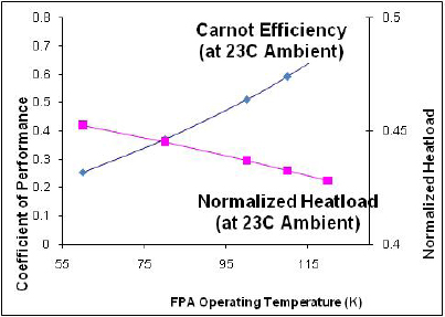
FIGURE 4-57 Impact of FPA operating temperature. SOURCE: D. Rawlings, DRS Technologies, Dallas, Texas.
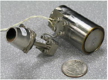
FIGURE 4-58 Advanced integrated Dewar cooler assembly. SOURCE: DRS Technologies, Dallas, Texas.
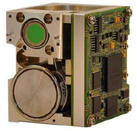
FIGURE 4-59 High-operating-temperature IDCA camera core. SOURCE: DRS Technologies, Dallas, Texas.
IDCA designers have taken advantage of these increasing array operating temperatures to develop lighter and lower power IDCAs. IDCAs with 640 × 480 pixel mid-wave IR (MWIR) detectors operating on as little as 2 W of input power at room temperature are being incorporated into IR sensor systems. One such IDCA is shown in Figure 4-58. Figure 4-59 shows a complete camera core based on a version of that IDCA. This module is about 2 × 2 × 2 inches, including the video processing electronics and runs on less than 5 watts of input power.
Conclusion 4-18: Cooling detector arrays such as those required for HgCdTe avalanche photodiodes operating in the mid-wave infrared band are not a major impediment from a size and power consumption standpoint. Already, state-of-the-art Dewar-cooler technologies, particularly those based on linear drive technology, are getting as small as 5 × 5 × 5 cm and power consumption of a few watts, comparable to those of thermoelectric coolers used for cooling detector arrays to 230 K. MEMS-based coolers are under development that will further reduce the size and power requirements.
Telescopes are often used on both transmit and receive. A single aperture for both transmit and receive, called a monostatic system, may be used. In a monostatic system, an approach must be developed for T/R isolation. If near-field reflections feed back into the receiver, it can be damaged or blinded. Alternately, in a bistatic system, separate apertures are used for transmit and receive. Bistatic systems do not have much of a T/R isolation issue since the apertures do not share common optics. Near-field reflections in theory could cause an isolation issue. For image plane imaging, optics are needed to transfer the captured field from the pupil plane to a focus at the image plane. Apertures can be various sizes, depending on need. No optics are required for pupil plane imaging, at least in theory. The received signal can be captured directly without using any telescope. In reality a telescope may be used to magnify the effective size of the receive focal plane array. While there is no need in this report to discuss the various types of telescopes, there is value in discussing the idea of arrays of subapertures. That approach is considered in the MIMO section in Chapter 3.
As will be described in more detail in Chapter 5, the atmosphere affects active EO sensors in three main ways: absorption, scattering, and refractive index variations (which can cause beam spreading or fluctuations). For active EO sensors these effects occur both for the illumination beam and for backscatter from the object being viewed by the receiving sensor. This section will describe methods to correct for distortion in active imaging caused by variations in the index of refraction of the atmosphere.
The effects of atmospheric turbulence are discussed in Chapter 5; they can be described as either thin turbulence or extended turbulence (see Figure 5-11). Adaptive optics systems can provide phase compensation for thin turbulence and some compensation for extended turbulence.
Adaptive Optics Systems
If the receive optics for a sensor are larger than the Fried parameter r0 of the atmosphere,167 an adaptive optics mirror can be put in the receive path to compensate for phase distortions. If the transmit optics are larger than the r0 of the atmosphere, again adaptive optics can be used to compensate and therefore to form a beam with less divergence. There are two main parts to any adaptive optics system. One part is the device that actually imposes the phase shift. This can be a mirror with many actuators behind it, or it can be a liquid crystal device or some other device to modulate phase. Adaptive optics mirrors may use electro-strictive (lead magnesium niobate, or PMN) actuators, piezoelectric-driven actuators, or other approaches. The second part is the control system to decide what phase shifts to impose. To determine what phases need to be imposed, the incoming signal is first measured. While multiple measurement instruments may be used, the most popular is the Shack Hartman sensor, shown in Figure 4-60. A second method of determining the required phase shift is a metric that judges the quality of the compensation. One such approach is called stochastic parallel gradient descent, SPGD, where increments toward an ideal metric are chosen along a gradient.
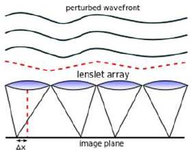
FIGURE 4-60 Shack Hartman wavefront sensor. SOURCE: By 2pem (Own work) [CC-BY-SA-3.0 (http://creativecommons.org/licenses/by-sa/3.0)], via Wikimedia Commons. http://en.wikipedia.org/wiki/Adaptive_optics, downloaded May 17, 2013.
____________________
167 The Fried parameter r0 is a measure of the effects on the quality of optical transmission through the atmosphere attributable to random inhomogeneities in its refractive index. It is defined as the diameter of a circular area over which the root-mean-square aberration due to passage through the atmosphere is equal to 1 radian. As such, imaging from telescopes with apertures much smaller than r0 is less affected by atmospheric inhomogeneities than by diffraction due to the telescope’s small aperture. However the imaging resolution of telescopes with apertures much larger than r0 (i.e., all professional telescopes) will be limited by the turbulent atmosphere, preventing the instrument from approaching the diffraction limit.
Another issue for an adaptive optics system may be having a point source to use as a guide for finding the optimum phase corrections. Sometimes an artificial point source is created, called a guide star.168
Schemes for Countering Extended Turbulence
Extended turbulence phase changes away from the pupil plane will result in amplitude changes at the pupil plane. Adaptive optics mirrors do not exist that change both phase and amplitude. When amplitude is changed it only decreases, creating a loss to be avoided. An alternative method of compensating for extended turbulence can occur for coherent imaging, whether it is spatial or temporal heterodyne. Once the field is captured at the pupil plane, virtual phase screens can be inserted in the computer at various ranges, and a sharpness metric can be used to judge the influence of the phase screens. These phase screens can be changed until an image with the best sharpness is reached.
One limit is the amount of beam spreading that can be tolerated for the illuminator beam. If flash illumination is used, then this is not a difficult limit. Assume even a 32 × 32 pixel FPA on receive. This means the illuminator beam can be 32 times larger in angle than a pixel, and the illuminator aperture can be 32 times smaller than the receive aperture. For a 20 cm receive aperture the transmit aperture can be less than 1 cm. Another way to think of this is that the Fried parameter can be less than 1 cm without interfering with the illuminator beam.
Another limit is the turbulence on receive. This will limit angular resolution. The diffraction on receive will be limited to the diffraction associated with an aperture diameter equal to the Fried parameter unless some form of compensation is employed. If an adaptive optics device were invented that could not only impose an array of phase changes on an incoming beam, but could also amplify or decrease the signal level in each pixel, then it would be possible to physically compensate for extended turbulence.
Conclusion 4-19: Any long-range active EO sensor will be limited by the atmosphere. The amount of limitation will vary from hour to hour and day to day. Atmospheric compensation can extend the operational range.
Conclusion 4-20: The ability to compensate for extended turbulence will greatly aid long-range active EO sensors.
PROCESSING, EXPLOITATION, AND DISSEMINATION
Processing, exploitation, and dissemination (PED) refers to the set of steps required to transform sensed photons into usable information. The processing step refers to the initial transformation of sensed photons into an image that, in turn, can be exploited in the context of an application such as robot navigation. The dissemination step refers to delivery of the information to its ultimate consumer(s)—for example, analysts seeking to understand an environment using change detection on a time series of images.
There may be multiple types of processing involved, for example, image formation from ROICs (see Figure 4-61), followed by image compression to reduce bandwidth required for real-time dissemination of imagery from an airborne sensor. Table 4-5 provides some PED requirements for some selected ladar applications.
____________________
168 See http://en.wikipedia.org/wiki/Laser_guide_star, download May 17, 2013.
TABLE 4-5 PED Requirements Versus Selected Application Domains
| Application | Possible platform | Processing | Exploitation | Dissemination |
| Surveillance | UAV | Image formation and refinement, image/video selection and compression | Precise positions for objects and actors in real-time | High bandwidth desirable, but not easily achievable with RF |
| Mapping | Airborne imager | 3-D image formation, registration to knit multiple swaths together | Precise 3-D maps of terrain, e.g., urban terrain | Can be gathered and stored until return to base |
| Local navigation | Driverless automobile | Image formation | Avoiding obstacles in real time | Not applicable; intended for local use |
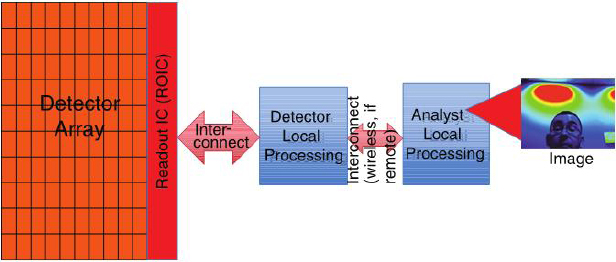
FIGURE 4-61 Abstract model of steps from detector to analyst. SOURCE: National Research Council, 2010, Seeing Photons: Progress and Limits of Visible and Infrared Sensor Arrays, The National Academies Press, Washington, D.C., Figure 4-9.
Target Tracking
Target tracking is a general technique useful in a variety of application domains. An easy to understand example is tracking of pedestrians and other vehicles in autonomous vehicle navigation. Because ladar is much more precise than radar for this application, it could generate reliable trajectories.
Target tracking169 first involves detection and acquisition. Once a target is acquired, the illuminator must somehow be periodically directed toward the target as its direction and velocity are tracked, to guarantee that sufficient reflected information is available for real time track maintenance.
____________________
169 C. Grönwall, G. Tolt, D. Karlsson, H. Esteki, J. Rydell, E.E. Armstrong, and J. Woods, 2010, “Threat detection and tracking using 3D FLASH ladar data,” Proc. SPIE 7696: 76960N.
Various processing schemes can be employed, from tracking classified objects (object classification is discussed in the section below) to simply tracking centroids of moving objects.170
Target Classification
Ladar target classification basically consists of image matches against a set or sets of known characteristics. The goal is often not an exact match, which would be difficult, but rather a best match or a match within a known threshold or error bound. A commercial use might be pedestrian detection for an autonomous vehicle.
Ladar target classification is an active area of research, with a variety of recent advances reported in the technical literature—for example, using ensembles of classifiers171 or using machine learning techniques such as support vector machines(SVM).172
Developing 3-D Maps
Ladar has found a variety of mapping applications, some of which exploit the ability of the technology to produce 3-D imagery. Examples include archeology,173 forestry,174 and geology.175 Mapping is typically performed as an aerial surveying activity; data are collected and partially processed, then stored on the aircraft. The recorded survey data are then post-processed; e.g., swaths are combined into a map and then analyzed.
3-D Target Metrics
For monochromatic 2-D imagery the National Imagery Interpretability Rating Scale, NIIRS, rating is used extensively to characterize image quality. Leachtenauer et al.176,177 empirically determined a method to calculate the NIIRS rating using various image metrics, such as the ground sample distance (GSD) and the relative edge response (RER).
____________________
170 P. Morton, B. Douillard, and J. Underwood, 2011, “An evaluation of dynamic object tracking with 3D LIDAR,” Australasian Conference on Robotics and Automation (ACRA), Melbourne, Australia: Australian Robotics and Automation Association (ARAA).
171 Z.-J. Liu, Q. Li, Z.-W. Xia, and Q. Wang, 2012, “Target recognition for small samples of ladar range image using classifier ensembles,” Opt. Eng. 51(8): 087201.
172 Z.-J. Liu, Q. Li, and Q. Wang, 2013, “Random subspace ensemble for target recognition of ladar range image,” Opt. Eng. 52(2): 023203.
173 F. Diep, 2012, “How lasers helped discover lost Honduras city,” TechNews Daily, June 7, http://www.technewsdaily.com/5837-lasers-helped-discover-lost-honduras-city.html, accessed May 30, 2013.
174 R.A. White and B.C. Dietterick, 2012, Use of LiDAR and Multispectral Imagery to Determine Conifer Mortality and Burn Severity Following the Lockheed Fire, U.S. Forest Service, General Technical Report PSW-GTR-238, pp. 667-675, http://www.fs.fed.us/psw/publications/documents/psw_gtr238/psw_gtr238_667.pdf.
175 R.A. Haugerud, D.J. Harding, S.Y. Johnson, J.L. Harless, C.S. Weaver, B.L. Sherrod, 2003, “Highresolution lidar topography of the Puget Lowland, Washington,” GSA Today, Geological Society of America, June.
176 J.C. Leachtenaur, W. Malila, J. Irvine, L. Colburn, and N. Salvaggio, 1997,” General image quality equation: GIQE,” Applied Optics 36(32): 8322.
Leachtenauer et al. later used the same empirical methodology applied to infrared images.178 Thurman and Fienup provided physical explanations for many of the parameters in the General Image Quality Equation (GIQE).179 Equation 1 is a generic version of the GIQE. Various constants can be used in this equation, representing somewhat different forms of the GIQE.
![]()
where NIIRS is the image quality rating assigned in accordance with the National Image Interpretability Rating Scale, RER is the relative edge response, J is the mean height overshoot caused by edge sharpening, G is the noise gain resulting from edge sharpening, and SNR is the signal to noise ratio. Recently Kammerman wrote a draft of a paper developing an information theoretic approach to calculate the NIIRs rating for monochromatic 2-D images, as compared to an empirical method.180 Ideally, this information-based theory would be a better predictor of NIIRS ratings for monochromatic visible imagery and would also provide a path to generate useful metrics for other imaging modalities, such as IR imagery, radar, and 3-D ladar imagery. At this time, there are no good 3-D metrics allowing a comparison of various 3-D imaging sensors, much less allowing them to be compared against other sensing modalities.
Conclusion 4-21: It would be very useful to be able to compare the value of various 3-D images, especially if they could also be compared against other sensing modalities.
Recommendation 4-1: Three-dimensional metrics should be developed in such a way that the ability of a given sensor to perform a given function can be compared against the ability of another sensor to perform the same function. 3-D imagery can be developed in multiple ways: for example, using stereo from passive sensors vs. using a 3-D active EO sensor, or using 3-D ladar vs. interferometric synthetic aperture radar. Metrics are needed to be able to compare the products of different sensing modalities.
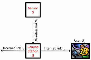
FIGURE 4-62 Communication model for ladar used for ISR on a UAV.
____________________
178 J.C. Leachtenauer, W. Malila, J. Irvine, L. Colburn, and N. Salvaggio, 2000, “General image-quality equation for infrared imagery,” Applied Optics 39(26): 4826-4828.
179 S.T. Thurman and J.R. Fienup, “Analysis of the general image quality equation,” Proc. of SPIE 6978 69780F-1.
180 G.W. Kamerman, “On Image Information Density,” Optical Engineering to be published, 2013.
Data File Size, Compression, Dissemination, and Communication Bandwidth Requirements
A given sensor produces data at some rate, and then the application domain dictates whether data is stored or communicated. Whether stored or communicated, it may be compressed to a more compact form, ideally with minimal loss of information content. One reason for compression of stored data might be to make better use of available storage—for example, to store mapping data for a greater area of coverage or to extend mission duration. As Table 4-5 suggests, navigation of completely autonomous vehicles faces very little in the way of PED challenges, as the data is both produced and consumed locally by the navigation subsystem of the vehicle.
On the other hand, as discussed in an earlier NRC report Seeing Photons,181 unmanned aerial vehicles (UAVs) used for intelligence, surveillance and reconnaissance (ISR) may represent the most challenging ladar application for communications, as the data are meant to be consumed at a considerable distance from where they are gathered; an abstract view of this application is shown in Figure 4-62.
Since the Wireless Link W is typically highly constrained relative to the sensor capabilities, compression is often employed between the sensor and the ground station. There are many forms such compression can take, including sampling, lossy compression, image compression, video compression, and compressive sensing. There is an interesting tradeoff between placing more computational intelligence in the sensor to provide sensor-side analysis and the SWaP considerations of the airborne sensor.
Fusion or Synergy with Other Sensing Modalities
Ladar is extremely powerful as a complement to other sensing capabilities. For example, some combination of GPS, radar, video cameras, and ladar was used by almost all entrants in the DARPA Grand Challenges and the Urban Challenge to maximize the operating capabilities of the self-driving vehicles. The absolute frame of reference for navigating the vehicle could be determined to a reasonable degree of precision with differential GPS, but obstacle detection is best performed with one of the other sensor technologies.
Conclusion 4-22: Ladar may be most powerful when viewed as part of a system of complementary sensors rather than as a stand-alone multifunction sensor.
Conclusion 4-23: Use of ladars may be most cost-effective where they offer sensory capabilities (such as precision stand-off ranging and vibrometry) that are difficult for other sensors to achieve.
Computational Requirements, Processing Throughput, and Processor SWaP
Figure 4-63 shows the data processing steps associated with the ALIRT 3-D ladar system discussed in Chapter 2. One set of steps182 in image formation from Jigsaw183 data are illustrated in Figure 4-64. Each of these steps can consume substantial computing time (as shown in Table 4-6), which affects the total delay from the detection to the image or other exploitable data product.
____________________
181 National Research Council, 2010, Seeing Photons: Progress and Limits of Visible and Infrared Sensor Arrays, The National Academies Press, Washington, D.C.
182 P. Cho, H. Anderson, R. Hatch, and P. Ramaswami, 2006, “Real-time 3D ladar imaging,” Lincoln Laboratory Journal 16(1): 147.
183 R.M. Marino and W.R. Davis, 2006, “Jigsaw: a foliage-penetrating 3D imaging laser radar system,” Lincoln Laboratory Journal 15(1): 23.
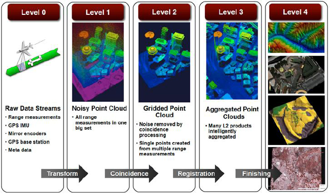
FIGURE 4-63 ALIRT data processing steps. SOURCE: Dale G. Fried, 2013, “Photon-counting laser radar development at MIT Lincoln Laboratory,” April 24. Courtesy of MIT Lincoln Laboratory.
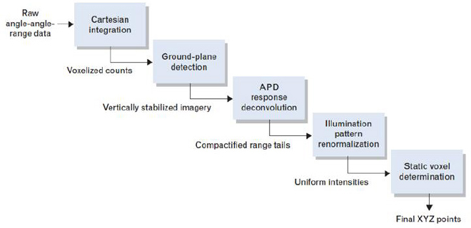
FIGURE 4-64 Steps in processing Jigsaw data. SOURCE: P. Cho, H. Anderson, R. Hatch, and P. Ramaswami, 2006, “Real-time 3D ladar imaging,” Lincoln Laboratory Journal, 16(1): 147. Reprinted with permission of MIT Lincoln Laboratory.
Since the goal of this system is real-time 3-D imagery, 8.2 s of compute time per second of the data stream is unacceptable. Therefore, additional computing resources are brought to bear in a mode of computing called parallel processing, where multiple computations are carried out simultaneously. Fortunately, the algorithms allow parallel operation, and a set of 10 computers, as illustrated in Figure 4-65, can be employed to reduce the computation time to enable real-time operation.
TABLE 4-6 Computing Resources Consumed per Second of Imagery
| Algorithm Task | Processing Time/Real Time |
| Raw data input | 0.1 |
| Cartesian integration | 3.0 |
| Ground detection | 0.2 |
| Response deconvolution | 3.2 |
| Static voxel determination | 1.1 |
| XYZ file output | 0.7 |
| Total | 8.2 |
| NOTE: Single processor timing results measured on a 3 GHz Pentium machine. SOURCE: Peter Cho, Hyrum Anderson, Robert Hatch, and Prem Ramaswami, 2006, “Real-time 3D ladar imaging,” Lincoln Laboratory Journal, 16(1): 147. Reprinted with permission of MIT Lincoln Laboratory. |
|
FIGURE 4-65 Parallelization of computation in Figure 4-64. SOURCE: Peter Cho et al., op. cit. Reprinted with permission of MIT Lincoln Laboratory.
FIGURE 4-66 Data reduction in a compute node from Figure 4-65. SOURCE: Peter Cho et al., op. cit. Reprinted with permission of MIT Lincoln Laboratory.
An additional benefit of some steps is that they reduce the data rate through the system to a rate that is more sustainable by serial processing techniques, in preparation for delivery of imagery, as shown in Figure 4-66.
Currently, data from high-performance ladar sensors requires parallel processing. Processing capabilities with abundant parallelism, such as many core graphics processor units (GPUs), are commercially available, but SWaP requirements for UAVs are not a commercial consideration. DARPA’s Power Efficiency Revolution for Embedded Computing Technologies (PERFECT) Program184 has UAVs as a target application and seeks methods to move from the current energy performance level of 1 GFLOP185/W to greater than 75 GFLOPS/W. Interconnect architectures for some abundantly parallel machine architectures may be ill-suited to processing some sensor streams, but for others the performance gains may be substantial.
____________________
184 See http://www.darpa.mil/Our_Work/MTO/Programs/Power_Efficiency_Revolution_for_Embedded_Computing_Technologies_(PERFECT).aspx.
185 1 GFLOP is 109 floating point operations per second.


