
6
Photonics and the Nanoworld
How will we control and exploit the nanoworld? The scale of the nanoworld is smaller than a wavelength of visible light. This places it between the classical world of microscopic objects such as living cells and the quantum world of atoms and molecules. Nanoscale structures are rich in promise for novel AMO research because they have nonintuitive but useful physical, chemical, and biological properties that come from their submicroscopic size. These tiny structures present unique opportunities to tailor material properties for a tremendous range of potential applications. In optical physics, nanoscience promises efficient optical switches, light sources, and photoelectric power generators. In the next decade, new nanomaterials may dramatically improve optical microscopes or reduce the feature size in semiconductor chip fabrication. Other applications include precisely periodic nanostructured materials or photonic crystals, single-photon sources and detectors, nanostructured electron emitters for flat-panel displays and television screens, sensors for environmental monitoring, and biomedical optics, with applications such as killing cancerous cells via localized optical absorption and heating.
The nanoworld exists at the interface between the classical and quantum worlds, providing the opportunity to explore the transition between these worlds, as well as the prospect of using features from both worlds to produce exciting new behaviors and technology. Nanoscience, the study of the nanoworld, is an inherently multidisciplinary field of research that requires concepts, methodologies, and tools from a broad range of scientific disciplines. AMO physics is a touchstone for understanding many of the new phenomena of nanoscience and has provided numerous tools for performing forefront research. In return, nanoscience promises to provide fundamental and technological breakthroughs that will benefit both the scientific community and society at large. AMO physics is already benefiting from new tools that are enabled by breakthroughs in nanofabrication and nanoengineering. This chapter highlights specific opportunities that lie at the interface between nanoscience and AMO physics, with a particular emphasis on photonics.
The allure of nanoscience can be understood by considering what happens if a macroscopic gold nugget is divided into ever smaller pieces.1 At first, the piece of gold will retain all of its typical characteristics—it simply gets smaller. When the pieces reach a few micrometers in size, we are no longer able to distinguish individual particles with our eyes. However, given enough of them, we still see gold dust. However, when the particles reach a size of -100 nm, something very dramatic happens: The particles change color. For particle diameters between approximately 100 and 30 nm (i.e., for particles containing between approximately 30 million and 1 million gold atoms) the particles change from red or yellow, to green or blue. The particle’s color is determined by its size. Quite amazingly, these colored gold particles have been known since the Middle Ages, when they were used to make beautiful colors in stained glass windows. Of course, the medieval artisans did not know that they were using nanotechnology, or even why the gold produced the colors it did: They just knew that a particular process produced a beautiful effect (see Figure 6–1).
It is only in the last few years that we have begun to understand the size-dependent changes that occur in gold and other metallic nanoparticles. The size of a nanoparticle determines the character of its surface plasmons, a type of collective motion of the electrons within the particle that gives rise to its color. The strong dependence of the particle’s characteristics (in this case its color) on the size of the particle is one of the key features of nanoscience. With our understanding of the nature of the color changes comes the opportunity to tune the particles to achieve the behavior we desire.
OPPORTUNITIES IN SIZE-DEPENDENT DESIGN
The nanoworld is intriguing because it is not just the color of nanoparticles that depends on size. At the nanoscale, a wide range of physical, chemical, and even biological properties can be strongly dependent on the particle size. We expect that by working at this scale, we will soon be able to design and engineer structures with a tremendous variety of desirable features. This is exactly what nature does in the inner workings of every cell. Proteins are nanoscale molecules that are assembled by nanomachines called ribosomes, which connect a series of amino acid molecules together according to a pattern furnished by RNA, another nanoscale molecule. Each protein is essentially a nanoengineered molecule that has been optimized to perform specific cellular functions. A typical cell is filled with numerous nanomachines that serve a multitude of functions, including regulation
|
1 |
For more information, see Mark Ratner, Introduction to Nanoscale Materials Behavior—Why All the Fuss? Available at <http://www.blueskybroadcast.com/Client/ARVO/trans/arvo_ratner_RF_OK.pdf>. |
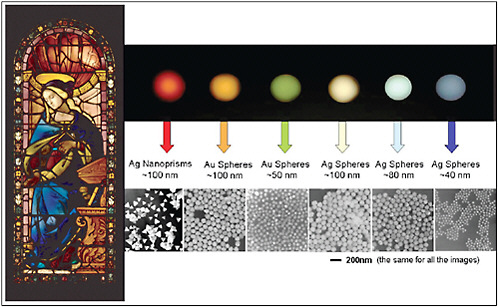
FIGURE 6–1 Left: Gold and silver nanoparticles are responsible for some of the beautiful colors in stained glass windows from medieval times. SOURCE: National Gallery of Art, Washington, D.C. Right: The colors of the gold and silver nanoparticles vary because of their different size, shape, and composition. SOURCE: Chad A.Mirkin, Institute for Nanotechmology, Northwestern University. These figures were taken from a slide in a presentation entitled “The Shifting Plate Tectonics of Science” by Arden L.Bement, Jr., Director, National Science Foundation, at the American Ceramic Society, Baltimore, Maryland, April 10, 2005, available at <http://www.nsf.gov/news/speeches/bement/05/alb050410_ceramicsociety.jsp>.
of the passage of food and waste through the cell membrane, generation of fuel for cellular functions, recognition of invading viruses, and full replication of the cell itself. Indeed, it has been said that the nanoscale is the design scale of nature. The amazing power of cellular machines has long provided inspiration to scientists. With the growth of nanoscience, we are in a position to develop and implement an extraordinarily broad range of new bioinspired materials, catalysts, and machines. One of the most exciting of these is the possibility of creating new power sources based on the light-harvesting photosynthesis machinery of plants.
The recent explosion of interest in nanoscience and nanotechnology has been fueled by the development of a host of new capabilities for visualizing, constructing, and manipulating matter at the nanoscale. Broadly speaking, nanoscience and nanotechnology involve three basic themes:
-
Research and development at the atomic, molecular, and macromolecular level involving length scales of approximately 1 to 100 nm (approximately 50 atoms to 50 million atoms);
-
The creation and use of structures, devices, and systems that have novel properties and functions as a result of their size; and
-
The ability to control or manipulate light and matter on the atomic scale.
The committee expects that in the coming decade, nanoscience will lead to tremendous advances for both science and society. In what follows, it describes some of the rapidly evolving approaches to visualize, manipulate, and ultimately harness the nanoworld that are enabled by AMO physics.
VISUALIZING THE NANOWORLD
The construction of our eyes allows us to see visible light or, more generally, electromagnetic radiation with wavelengths between approximately 400 nm (violet) and 750 nm (red). The wavelength of the light limits the ultimate size of an object that we can directly see using conventional optics. Thus, even with the best optical microscopes, it is not possible to resolve objects less than approximately 400 nm apart, because the wavelength of the light is longer than the separation, and the two objects therefore appear blurred together. If this is the case, how can we visualize the nanoworld? In this section, three different approaches to answering this question are discussed, each of which involves tools from AMO physics: reducing the wavelength, using scanning probe microscopies, and exploiting nanotechnology to build a better microscope.
Reducing the Wavelength
One route to improved resolution is to reduce the wavelength of the light used for viewing. Shorter wavelength light, corresponding to the ultraviolet and x-ray regions of the electromagnetic spectrum, provides better resolution than conventional optical microscopes. To date, soft x-ray microscopes have achieved a resolution of a few nanometers. In principle, shorter wavelength, harder x rays should allow even better resolution, but to date such microscopes have been limited to a resolution of ~20 nm. This resolution is limited not by the wavelength but rather by the ability to fabricate the appropriate x-ray lens (known as a zone plate) that is used to focus the x rays. Advances in nanofabrication techniques will one day override this limitation, allowing x-ray microscopes with subnanometer resolution to be built.
Often objects viewed with ultraviolet light or x rays look much different than when they are viewed with visible light. In general, visible light interacts with the
most loosely bound electrons in molecules, while x rays interact with the most strongly bound electrons. The former tend to be delocalized over the molecule, while the latter tend to be localized on individual atoms. By illuminating the sample with particular wavelengths of light, or by detecting fluorescence at particular wavelengths, it is possible to use different techniques to map out the spatial distribution of different elements in the sample. For example, it is possible using a hard x-ray microscope to map out the spatial distributions of different elements within a single cell. Other techniques can be used to provide even more information. For example, nonlinear optical techniques such as multiphoton excitation and Raman spectroscopy are now being used to image specific chemicals, again with subcellular resolution, and to study time-dependent processes involving these chemical species. Although these advances are expanding rapidly into an increasing number of scientific disciplines and technological applications, it is particularly noteworthy that AMO science provides essential underpinnings for understanding the new contrast mechanisms and optical techniques.
Beyond x rays, can the resolution be pushed even higher? The quantum mechanical nature of matter gives both particle and wave character to light and matter. The heavier a particle and the higher its kinetic energy, the smaller its de Broglie wavelength. Electron microscopes use high-energy electron beams to view the sample: In this case the de Broglie wavelength is so short that it no longer limits the resolution. The appearance of samples viewed with an electron microscope is determined by the details of the electron-matter interactions, which have long been a subject of great interest for AMO physics. Using even heavier particles—namely, whole atoms—researchers in atom optics are working to create a new, high-resolution atom microscope with an ultrashort de Broglie wavelength.
Scanning Probe Microscopes
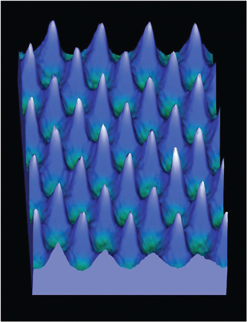
One approach to imaging the nanoworld is to dispense with the idea of “seeing” altogether and to use an alternative means of visualization. As an example, consider having fingers only a nanometer in diameter and slowly running them across some molecules sitting on a surface. The displacement of these fingers as they cross the molecules would be similar to that of the tip of an atomic force microscope (AFM), which allows one to create a nanoscale map of the surface roughness by measuring the deflection of an ultrafine tip on a cantilever as it is “dragged” across the surface. An example is shown in Figure 6–2. The AFM is but one of a wide range of scanning probe microscopies, each of which relies on a different molecular-scale effect for its contrast mechanism. The intermolecular forces and tunneling phenomena that provide the contrast mechanisms for these microscopies can best be understood using concepts from AMO physics.
The scanning tunneling microscope (STM) is a particularly powerful tool that relies on the measurement of tiny electrical currents that pass between the tip and the surface, with changes in these currents reflecting the local densities of electrons on the surface. Such STMs have been used to map out the positions of individual atoms on the surface of a crystal, as well as the positions of atoms within a molecule. Perhaps even more exciting, the tips of these STMs have been used to move and position individual atoms sitting on a crystal surface, allowing the creation of controlled structures with atomic dimensions.
An optical version of these scanning probe microscopies also exists—namely, near-field scanning optical microscopy (NSOM). This technique provides subwavelength resolution that is well below the conventional limit of optical microscopy. In one form of NSOM, the tip used in an AFM or STM is replaced by an optical fiber tapered to a tip approximately 50 nm across; this tip is positioned a few nanometers above the surface of interest and then scanned across it. Laser light is sent down the fiber and tunnels out of the tip, illuminating the sample over an area approximately equal to the diameter of the tip. Scattered light or fluorescence from the sample is then detected, allowing an optical image with approximately 50-nm resolution when a laser wavelength of 500 nm is used. This approach has also been pursued using ultrafast lasers, allowing the study of time-dependent phenomena with unprecedented spatial resolution. Many additional new techniques, such as multiphoton microscopy and ultrafast confocal microscopy, are now being developed to apply optical methods to probe nanoscale and even single-molecule processes in exquisite detail.
Using New Materials to Build a Better Microscope
Can nanoscience enable us to build a better microscope? One intriguing possibility is the development of a new generation of microscopes using properties of light that were previously inaccessible. Conventional lenses have what is known as a positive index of refraction. When light passes from one medium to another (e.g., from air to a quartz lens), the ray is bent by an angle that depends on the difference between the refractive indices of the two materials. These positive index lenses create images by capturing the propagating light waves emanating from an object and bending them into a focus. However, the resolution is limited to roughly one-half the wavelength of the illuminating light—that is, the diffraction limit. The electromagnetic field emanating from an object includes not only propagating waves but also near-field evanescent waves that decay exponentially as a function of distance away from the object. These evanescent waves carry the finest details of the object, but unfortunately they cannot be recovered by conventional positive-index lenses—and all naturally occurring materials have a positive index.
Theorists predicted that a material with a negative refractive index could capture and refocus these evanescent waves, and in 1968 it was proposed that a perfect lens, or “superlens,” could be made from a negative-refractive-index material. In such a superlens, the electromagnetic waves reaching the surface of the negative-index lens excite surface plasmons, which enhance and recover the evanescent waves. Experiments have demonstrated the existence of materials with a negative index of refraction—called left-handed materials—for microwaves (see Figure 6–3). Researchers using a thin silver slab as a superlens were able to image objects as small as 40 nm, smaller by a factor of 10 than the limit of current optical microscopes. This important experimental advance not only resolved a controversial question about the nature of these negative-index materials but also opened the door to a variety of novel applications, including higher resolution optical imaging, nanolithography, and optical elements that exploit the evanescent waves of light.
CONSTRUCTING THE NANOWORLD
Synthesis at the nanoscale can proceed in two directions: starting on a larger scale and working down in size (top-down) or starting at the atomic scale and building up (bottom-up). A vast array of synthetic approaches using methods from physics, chemistry, materials science, and biology are rapidly being explored and developed, some of which combine aspects of both top-down and bottom-up design. What follows is only a brief overview of a few of the exciting possibilities for building structures in the nanoworld.
From the Top Down
One way to create nanostructures is to use optical lithography or laser ablation techniques to remove or add material to surfaces through a sequence of processing steps. The depth of removal or addition of material can readily be controlled at the level of single atomic layers. The width of features that can be written with these techniques is considerably larger. In addition to limiting the resolution achievable when viewing objects, the wavelength of light also places constraints on the resolution that is achievable when light is used to modify or write designs on surfaces using lithographic or ablation techniques. In particular, the resolution of the lithography that is required for manufacturing computer chips is limited by the wavelength of the light used. This is important because as the components on chips become ever smaller, new tools are essential to manufacture these chips. High-powered gas-discharge excimer lasers operating at ultraviolet wavelengths of ~193 and 157 nm are now commonly used in this process. AMO physics, in particular its insights into the electron-atom and electron-molecule collision processes in the
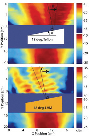
FIGURE 6–3 The terahertz frontier for negative-index materials. New sources and new applications of terahertz radiation have been forefront activities in AMO science over the past decade, and now this research is making connections to nanoscale materials. Many of the issues that arise when the size of the structure is comparable to the wavelength of the radiation have been understood and addressed for some time in studies using radiation at much longer wavelengths. For microwaves, the wavelengths are on the order of centimeters to millimeters, so that the construction of subwavelength structures is a considerably easier engineering task. As shown here, the first demonstration of a negative-index material was performed using microwave radiation. The top half of the figure shows microwave radiation passing through a wedge of a normal material (Teflon) and being refracted in a positive direction when it leaves the wedge. The lower half of the figure shows microwave radiation passing through a wedge of a negative-index material (left-handed material) constructed of wires and rings and being refracted in the opposite direction when it exits the material. In principle, materials with negative refractive indices at much shorter terahertz or even infrared wavelengths might be constructed using nanofabrication techniques. SOURCE: Andrew Houck, Yale University, reprinted figure with permission from Physical Review Letters 90, 137401 (2003). Copyright (2003) by the American Physical Society.
discharge and decay processes of the highly excited excimer molecules, played an essential role in the development of the high-power lasers that are now standard in the industry. The desire for still shorter wavelengths delivered from devices of reasonable size and efficiency has provided one of the strong motivations for tabletop x-ray sources.
Techniques based on scanning probe microscopies have also been used to modify surfaces at the nanoscale and may ultimately provide general-purpose techniques to do so. For example, light from a near-field scanning optical microscope tip can be used to induce photochemistry or to ablate materials from surfaces with nanoscale resolution. With new tools and techniques, our ability to modify materials at the nanoscale is rapidly growing. Even free atoms can now be manipulated at the nanoscale (see Figure 6–4), giving rise to the field of atom nano-optics, a subfield of the extensive domain of research involving the laser control of neutral atoms and molecules.
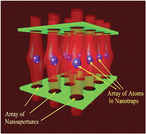
FIGURE 6–4 An array of atom traps. Light in the vicinity of holes and structures much smaller than its wavelength can have a number of interesting properties, allowing the creation of regions of high or low light intensity with sizes much smaller than this wavelength. With the appropriate structures (shown in green), these light fields can be arranged to produce a series of optical atom traps (atoms shown in blue) that are separated by distances much smaller than the wavelength of light. SOURCE: V.Balykin, V.V.Klimov, and V.S.Letokhov, Russian Academy of Sciences.
From the Bottom Up
For several decades, AMO physicists and physical chemists have studied how atomic and molecular properties change as one goes from a single atom or molecule to a bulk sample containing many millions of atoms or molecules. The study of clusters of carbon atoms revealed a special stability for the cluster containing 60 atoms. In this cluster, the atoms are arranged in the geometry of a miniature soccer ball only 0.7 nm in diameter. The discovery of this cluster, now known as buckminsterfullerene, was one of the significant events heralding the dawn of nanoscience, and the discoverers were awarded the Nobel prize in chemistry in 1996. The C60 molecule (“buckyball”) was soon followed by other fullerenes containing many more atoms of carbon and taking different shapes. One of the most interesting and prominent of these is the buckytube, or carbon nanotube. Nanotubes generally consist of hexagonal lattices of carbon atoms arranged spirally to form concentric cylinders. Single-wall nanotubes have a typical diameter of approximately 1 nm, while multiwall nanotubes consist of between 2 and 30 concentric tubes with an overall diameter of 30–50 nm. Carbon nanotubes are usually near-perfect crystals and range in length from a few tens of nanometers to several microns. They have unique properties which, like those of diamond, arise from their nearly perfect structure. Depending upon the details of this structure, a nanotube can act either as a highly conductive metal wire or as a semiconductor. Nanotubes have been used to build the first room-temperature transistor ever made from a single molecule and are widely expected to be the key ingredient for nanoelectronics that will vastly extend the power and shrink the size of computers and other smart devices. They are also efficient electron emitters, which has led to their application in flat panel displays, as described in more detail below.
A second example is provided by the many studies of small water clusters that have been performed in an attempt to understand the character of liquid water and ice. By using positively or negatively charged water clusters, it is possible to select species with a specific number of water molecules and thus to study the transition from molecular to bulk behavior in a step-by-step manner. Recent studies using infrared spectroscopy have led to new revelations about how such clusters arrange themselves to accommodate a positive or negative charge. As methodologies improve, an increasing number of powerful techniques can be applied to these studies, dramatically increasing our understanding of liquids. A final example is the strong size dependence observed for the catalytic properties of metal clusters. New techniques are now being explored to deposit size-selected clusters on surfaces and to characterize this size-selective catalytic activity. One day, such techniques could be scaled up to provide new industrial catalysts with improved efficiencies and selectivities.
EXTENDING THE PROMISE OF THE NANOWORLD
Many other breakthroughs can be anticipated based on further developments in nanoscience and technology. For example, there could well be significant improvements in solar energy conversion due to nanostructured solar collectors and new photovoltaic materials. There will likely be advances leading to more energy-efficient lighting. Nanoscience will doubtless have a broad impact in materials science as well. Indeed, we are entering a decade where stronger and lighter materials with novel characteristics will continue to improve efficiency and fuel use in transportation. New catalysts will provide low-energy chemical pathways that will be used both in the chemical industry to produce cheaper products and in remediation and restoration projects to break down toxic substances in the environment. We can imagine a safer and healthier world with extremely sensitive chemical, biological, and industrial sensors. Nanoscale titania and zinc oxide particles are already used in sunscreen formulations with improved UV protection, increased transparency (to eliminate their chalky appearance), and antibacterial activity.
To date, the most concentrated effort to apply the tools of nanoscale synthesis, characterization, and modeling has been in studies of the electronic properties of semiconductors and related materials. This effort has been driven primarily by the vital importance of semiconductors to information technology. Nevertheless, it is quite clear from this experience that for a wide range of materials, many other novel combinations of properties can be expected to emerge in the nanoscale regime. Here the committee describes some applications in optics and photonics.
Controlling Light with Photonic Crystals
One fertile area of research exploits the concept of the photonic crystal. Photonic crystals are periodic nanostructures that are designed to control and manipulate the flow of light in one, two, or three dimensions using the principles of diffraction (see Figure 6–5). For the crystals to work effectively, the spacing within the periodic structure must be the same order of magnitude as the wavelength of light—in other words, visible light requires periodicity on the nanoscale. One application of this field is the creation of new optical devices that confine light using internal microstructures. The best known of these materials are “holey” fibers—microstructured fibers that trap and concentrate light very effectively. Potential applications of this technology include studies of cavity quantum electrodynamics and development of quantum optical devices with capabilities such as emitting a single photon on demand. Controlling the emission of single photons has been a priority goal for application in quantum encryption systems, as discussed in Chapter 7.
Because true single-photon sources are not yet available, today’s commercial

FIGURE 6–5 The common blue morpho butterfly gets it iridescent blue color from diffraction off what is essentially a photonic crystal structure. SOURCE: The Butterfly Pavilion, Westminster, Colorado.
quantum cryptography systems rely on photons from attenuated laser pulses as an approximation of the single-photon state. However, the produced state has a nonvanishing probability of containing two or more photons per pulse, leaving such systems susceptible to eavesdropping through a beam splitter attack—this is what makes the need for advances in single-photon sources for quantum cryptography so important. The first electrically driven planar photonic-crystal laser was recently reported by a team at the Korean Advanced Institute of Science and Technology. This photonic crystal laser consisted of an array of holes passing through layers of InGaAsP multiple quantum wells (MQWs), which results in lasing in the near infrared at a threshold current about one hundred times lower than typical MQW lasers. This reduction in the threshold current suggests one approach to a zero-threshold laser or a source that delivers a single photon on demand. Another approach to making an all-optical router/buffer could take advantage of recent advances in all-optical switching in silicon photonic integrated ring resonator structures (see Box 6–1).
An interesting variation on the theme of controlling light with photonic crystals was recently demonstrated. In these experiments, two-dimensional arrays of 390-nm polystyrene nanospheres were created by trapping the particles with overlapping beams of light generated by scattering off a prism. These arrays show
|
BOX 6–1 All-Optical Switching in Silicon Photonic Integrated Ring Resonator Structures Using electron-beam lithography and plasma reactive-ion etching, researchers have constructed an all-optical silicon switch consisting of a straight waveguide (light-guiding channel) adjacent to a circular waveguide, or ring resonator with 450-nm-wide by 250-nm-high rectangular cross sections and a ring diameter of 10 microns. A 250-nm gap exists at the closest separation between the straight waveguide and the ring resonator. Ordinarily, information-carrying light pulses traveling in the straight waveguide would couple into the ring resonator. However, if the circumference of the ring resonator is a multiple of the wavelength of the light pulses, then the ring is resonant and effectively blocks the light pulses from coupling into the ring resonator. By using a control optical pulse of a different wavelength and focusing it on the ring resonator near the 250-nm gap, one produces enough optical absorption and subsequent photocreation of electrons to modify the refractive index of the ring to modify the resonance. Now out of resonance the light pulses are coupled from the straight waveguide into the ring resonator. Switching speeds as fast as 450 ps have been reported using this approach, which is orders of magnitude faster than the competing technology of thermo-optic switches. With modifications of this structure, one can easily imagine storing an optical pulse in this silicon ring resonator and switching it out as needed to produce the all-optical router/buffer described using a “slow light” approach (Box 4–1). |
many of the dynamical features of molecular crystals, such as surface diffusion, migration of defects, nucleation of phase transformations, and “Ostwald ripening”—where two arrays coalesce into one. Because the light can be used to control the positions of the nanospheres in the array, this new approach may prove to be a valuable method to assemble matter on the nanoscale.
Atomtronics
Atomtronics is a new technology enabled by nanoscience in which ultracold atoms are trapped and manipulated on or near a microelectronic chip. This atomchip amalgamation of cold atom and optical technologies on semiconductor chips will be an emerging area of nanoscience and nanotechnology in the next decade. The success of microelectronics has demonstrated the enormous potential of miniaturization for turning basic physics into applications. Today, researchers are exploring further miniaturization to nanometer and even atomic scales. The tiny clouds of ultracold atoms trapped and suspended barely above a semiconductor chip surface can behave as coherent matter waves under the influence of the electromagnetic fields in the microchip circuitry. The chip fields generate tiny forces
that can be used to guide and manipulate the matter wave. This presents opportunities for the construction of matter-wave interferometers on microchips, which may serve as sensitive probes for gravity, acceleration, rotation, and tiny magnetic forces, as well as analogs of transistors and other solid-state devices in the more distant future.
Nanotubes in Televisions
Success stories to date in the use of nanotechnology for real-wo rld applications include the recent entry of carbon nanotubes in the flat-panel display market. A new prototype nanoemissive display (NED) based on carbon nanotubes may challenge existing technologies of liquid crystal displays (LCDs), plasma displays, and organic light-emitting diode (OLED) displays. The key to the new NED is the ability to grow carbon nanotubes directly onto the display’s glass substrate. On a back plate only 3 mm behind each subpixel, a small structure containing about a thousand carbon nanotubes is arranged such that a properly applied voltage excites each nanotube, which in turn bombards the color phosphors with electrons. The new technology was recently demonstrated with full-color video, and it is estimated that a 42-inch NED would consume only 40 percent of the power of a similar-sized LCD.
Nanotechnology in Medicine
AMO researchers are merging state-of-the-art optical physics and nanoscience to make important strides in health and medicine. For example, treating cancer cells without destroying normal tissue has been a long-standing problem in oncology. While chemotherapy uses biochemical means to attack cancer cells selectively, it often destroys many faster-growing normal cells as well, leading to hair loss and more serious side effects. Researchers across the country are now attacking this problem using the unique properties of nanoscale materials.
One approach to the treatment of tumors involves the use of the same carbon nanotubes discussed above. Thousands of carbon nanotubes can easily fit into a typical cell, and they absorb near-infrared light that passes harmlessly through the rest of the cell. Electrons in the nanotubes become excited by the near-infrared light and release this excess energy in the form of heat. A solution of carbon nanotubes under near-infrared excitation can heat up to 70°C in as little as 2 minutes. When these nanotubes were placed inside the cells and irradiated with a near-infrared laser, the cells were quickly destroyed by the heat, while the light had no effect on the cells without nanotubes.
A second approach to cancer therapy involves the use of nanoshells: virus-sized,
metal-coated glass shells whose optical properties can be tuned to absorb or scatter specific colors of light (see Figure 6–6). It has been discovered that when gold-coated nanoshells are injected into the bloodstream, they selectively accumulate in tumors. By varying the diameter of the silica core (~100 nm) and the thickness of the surrounding gold shell (~10 nm) of these particles, the peak optical absorption can be tuned to the near-infrared. Irradiation by a fiber-coupled diode laser can lead to local temperature increases of up to 50°C. Researchers have found that tumors in nanoshell-treated mice disappear 10 days after this treatment, while tumors in animals without nanoshells continued to grow rapidly, suggesting that such local heating is very effective in destroying cancerous tumors.
As an ever more rapidly aging world population presents unique health-care
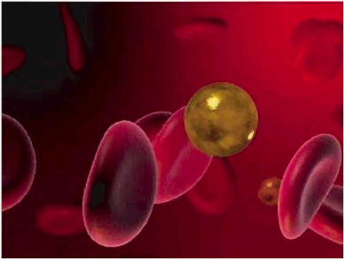
FIGURE 6–6 Gold nanoshells are made to either absorb or scatter light preferentially by varying the size of the particle relative to the wavelength of the light at their optical resonance. These nanoshells can be used to treat cancer in the upper regions of the lung. The nanoparticles specifically target the tumor and, upon excitation with near-infrared light, destroy only the cancerous tissue. SOURCE: Alliance for Nanohealth.
problems, new approaches for early detection and treatment of diseases will be required. Nanomedicine utilizing light-guided and light-activated therapy, with the ability to monitor real-time drug action, will lead to new approaches for more effective and personalized molecular-based therapy.
Nano-sized Sensors and Lighting
Nanospheres also have especially sensitive light-scattering properties that make them ideal for use in chemical sensors. The chemical properties of a tiny object like a biomolecule or a nanosphere can be revealed through Raman scattering of light. Owing to the minute amounts of energy left behind in the molecule, the Raman effect causes a tiny reduction in the frequency of light scattered by a chemical. These Raman frequency shifts are optical fingerprints of the chemical species. Nanospheres can be designed so that chemicals embedded in them or attached to their surface exhibit enhanced Raman scattering by a factor of up to a million. This capability creates the opportunity for many new, all-optical remote-sensing applications sensitive to just a few molecules of a drug molecule, disease protein, or other chemical agent.
The optical properties of nanostructures are also expected to have a significant impact on future energy needs—for example, energy consumption for lighting could be reduced by replacing current technologies (incandescent and fluorescent lighting) with solid-state lighting or OLEDs. The size dependence of optical properties at the nanoscale can also be exploited. For example, while bulk silicon has poor optical properties for optoelectronic devices such as solar cells or lasers, at small dimensions the band gap in silicon can be blue-shifted from the infrared to the visible spectrum; as a result, porous silicon exhibits remarkable room-temperature luminescence. Nanotechnology also has considerable potential to reduce the cost of photovoltaic cells, and recent work has demonstrated that thin-film cells based on nanoparticulate materials can be fabricated with reasonable efficiencies and stabilities.
In the next 10 years, exploration of the nanoworld will likely bring a veritable explosion of new science and technology. AMO physics will play an essential role in this exploration and will also reap the benefits of the developments that come from it.


