
6
INTEGRATED PROCESSING
The combining of two or more process steps into a single piece of equipment, or into a single operating system, under unified control is process integration. A simple example of process integration is the cleaning of a substrate surface by sputtering followed by sputter deposition of material onto the cleaned surface, all done in a single closed system. The operation of an oil refinery to produce gasoline from crude oil is a more complex example of process integration. This chapter presents some examples of integrated materials processing that use beam technology.
INTEGRATED PROCESSING IN MICROELECTRONICS
A number of factors are coming together today to accelerate the push toward integrated materials processing. In the area of integrated circuit and optoelectronic device fabrication, these incentives and needs include:
-
increased wafer size,
-
reduced feature size,
-
need for ultraclean wafer environment,
-
prevention of oxidation of work on exposure to air,
-
need for reduced inspection time,
-
reduced equipment and process expense,
-
need for quicker turnaround time,
-
need for more rapid changeovers,
-
increased process complexity,
-
reduced handling, and
-
in situ process control.
As illustrated in Chapter 4, beam processing is used extensively in the manufacture of state-of-the-art semiconductor circuits and optoelectronics. Most of these processes have been introduced as replacements for less accurate or more difficult to control process techniques. Integration of process steps and processing equipment is only beginning to occur in this industry, where the traditional processing techniques are batch oriented. Most of the process steps and process controls are centered around individual pieces of equipment in which the particular deposition, etching, patterning, and heating steps occur. Statistical process control techniques have been applied to identify the process capability of each step and to improve the repeatability and yield of the fabrication process.
Integrated Processing For Integrated Circuits
Fabrication of integrated circuits, as described briefly in Chapter 4, consists of a complex sequence of process steps that require high precision, repeatability, and cleanliness. During the past decade, circuit dimensions have decreased by more than a factor of 10 and circuit complexity has increased by more than 10 times, largely because of the improved processing capabilities
provided by beam technologies. These beam technologies have displaced previous techniques on a step-by-step basis; however, the general process flow is still batch oriented, as it was before the widespread introduction of beam technologies.
Traditional Integrated Circuit Processing Techniques
The reasons for the existence of a batch process flow relate to the economics of achieving cost-effective equipment utilization and throughput for time-consuming steps such as oxidation and diffusion and the economics of batch processing in wet chemical steps such as cleaning, etching, and photoresist removal. The capital equipment costs and throughput limitations of these steps still heavily favor batch processing whenever they are used. Significant effort has been expended on reducing the variability of the process steps across the batch. Wider process margins are required for batch-processed wafers than would be required for individually processed wafers if adequate control systems existed to repeatedly process individual wafers in a single-wafer system.
Because individual pieces of equipment have vastly different batch sizes and process times, the work-in-process inventory is large, the inventory is stored at many points in the process, and the cycle time is fairly long. Process control is centered on the individual piece of equipment and the process is related to the equipment. Most modern semiconductor process equipment has local microprocessor control of the process input variables, which allows several variations of the same process to be run with minimal operator intervention. Material flow between the process steps is accomplished by removing the wafers from one system, storing them in a cassette and box, manually transferring them to the next station, and then loading them into the next system. Because of the varying exposure times of the wafers between steps, there generally is a cleaning or surface treatment operation between any two major process steps. These cleaning operations add significantly to the processing complexity, time, and cost. They are, nevertheless, necessary because of the exposure of the semiconductor wafers to the ambient atmosphere.
Information flow between the process steps is sometimes computerized, but often measurements are made and recorded by paper documentation, which moves with the wafers. This information is rarely fed forward to modify the subsequent process step based on the results of the previous step. Measurements of results and modification of process steps on a wafer-by-wafer basis are not possible in the batch processing environment.
Advances Toward Integrated Processing
The economics of larger wafers, coupled with the requirements for more stringent cross-wafer uniformity and reduced feature size, have been major driving forces in the development of single-wafer or continuous flow beam processing equipment for the manufacture of integrated circuits.
The lithography process is a single-wafer process because a mask can be used only for printing one wafer at a time. Introduction of the wafer stepper, which has been the main driver for reduced geometries, has accelerated the move to larger wafers, thereby reducing the cost per exposure by amortizing the alignment and wafer handling time over a larger number of exposures. As wafer sizes increased, the uniformity of deposition and etching across a wafer in traditional batch beam processing systems became inadequate. Single-wafer systems have now been developed for high uniformity and repeatability across a single wafer. To prevent throughput problems, deposition and etch rates had to be dramatically increased at the cost of selectivity and
substrate damage. New processing techniques had to be developed for other process steps when single-wafer equipment was developed.
Single-wafer or continuous flow process equipment now exists for most of the process steps required for state-of-the-art integrated circuit fabrication. Dielectric and metal deposition systems that remove wafers from a cassette, process them, and reload them into a cassette are available. Likewise, cassette-to-cassette plasma etchers for dielectrics and metals also exist. Most aluminum etching is still done in batch-mode equipment, but automatic wafer handlers are available for loading and unloading. Photoresist and lithography equipment has long been cassette to cassette oriented. Most dry etching systems have some type of endpoint detection, so that the process is somewhat tolerant of etch rate variation and incoming material variations. Other systems have automatic control of the process variables, but little exists by way of real-time monitoring of the actual process results. Except for the 25-wafer cassette, no standardized interface exists for material flow from system to system. Several proposed standards are being developed at this time.
Integrated processing lines for single-product manufacturing (e.g., dynamic random access memories [DRAMs]) can be built to take advantage of continuous work flow when process flexibility is not required. Such a line can be configured by providing a separate piece of equipment for each process step, instead of performing many similar steps in one machine. For a typical metal-oxide semiconductor (MOS) process with 10 masking levels, 10 separate lithography cells would exist, one for each mask level. The material would flow continuously from station to station through the sequence of fabrication steps. High volume is required to justify the large capital expenditure for such a fabrication line, and, without significant improvement in flexibility and process control, such expenses cannot be justified for small-volume or applications-specific products. Even when such a process line is built, a major effort is required to interface the various pieces of process equipment that must transfer the material and information.
Integrated Processing Tools
In the past three years a few beam processing systems have been introduced that can perform multiple process steps. Such systems have become known in the semiconductor industry as cluster tools. The earliest tools were the multichamber etch or deposition systems. These systems allow sequential steps to be performed without cross-contamination, which results from the transfer of wafers from one station to another. Each process station can be configured to ''optimize'' the conditions for a given step. The systems are flexible, so that chambers also can be run in parallel or in any desired combination of serial and parallel steps. The etching of multilayer films, followed by photoresist strip, is a typical application for such cluster tools.
The development of integrated processing tools to do more complex fabrication sequences is limited by many factors, such as development cost, range of process expertise, unknown market requirements, and lack of equipment interface standards. The Modular Equipment Standards Committee (MESC), of the Semiconductor Equipment and Materials International (SEMI), was formed to develop standards for mechanical, utility, software, and control interfaces for future integrated processing systems. These standards will enable circuit manufacturers to choose the component systems necessary for their fabrication processes and have assurance that the systems can be integrated into a working whole. Nevertheless, it is expected that in the next 3 to 5 years, little will exist in integrated process tools beyond throughput-enhanced single-wafer systems. Significant problems of throughput, cost, uptime, real-time control, information flow, and process step development need to be overcome before significant use of integrated process tools will
occur. Extensive development programs could accelerate progress in this vital area (Design Test Manufacture, 1991).
These needs are recognized as important steps toward integrated processing in semiconductor electronics as exemplified by cooperative research efforts at the Semiconductor Research Corporation and SEMATECH for the semiconductor industry (consortia for the advanced development of IC technology, system architecture, and packaging, and for manufacturing processes and materials, and equipment development). In addition, the Engineering Research Center at North Carolina State University, funded by the National Science Foundation, has a focus on IC integrated processing. DARPA and the Air Force also have an active program (MMST) at Texas Instruments, Inc.
Applications For Integrated Processing Tools
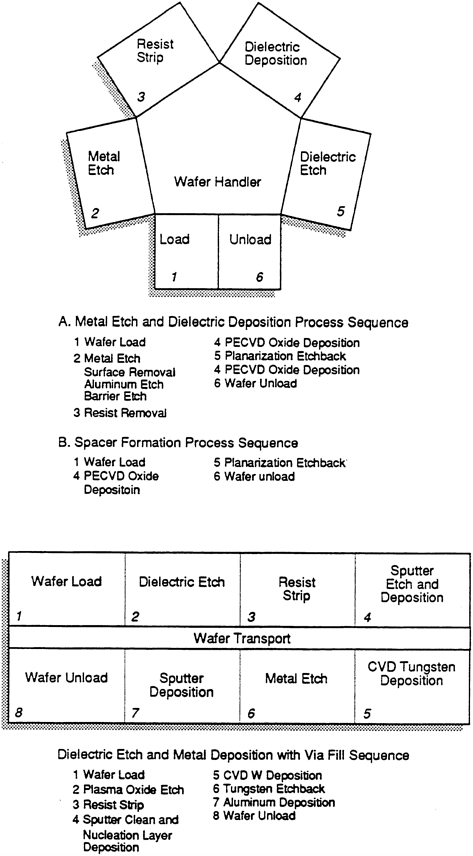
In evaluating potential uses for integrated processing tools, an assumption is made that the photolithographic steps will be done on optical steppers employing photoresist technology and wet chemical development. This means that each masking step will be done outside an enclosed-environment beam processing tool. The steps that could be performed by an integrated processing tool would consist of etching, stripping, cleaning, and deposition. The advantages of such sequences would be cleanliness, prevention of surface contamination from exposure to room atmosphere, reduced cycle time (compared to single-wafer systems), and the opportunity for improved control and quality from the ability to continuously monitor and adjust the process. Some examples of possible integrated processes are shown in Figures 6-1. An experimental system has been developed in Japan for the integrated processing of optoelectronic device structures.
INTEGRATED PROCESSING FOR METALS AND CERAMICS
Integrated processing systems are employed in the manufacture of some metallic and ceramic articles. Increasingly, machining steps are carried out by flexible machining systems (FMSs), which consist of a group of machine tools linked by an automatic materials-handling system and controlled by a computer. A workpiece is loaded onto a carrier or pallet and sent from one machine tool to the next, according to a specific manufacturing plan. Tools are changed automatically, and quality control is performed on-line with automatic measuring tools. Direct labor is kept to a minimum and often is restricted to loading and unloading workpieces from the FMS and periodic maintenance procedures. With the development of beam technologies, new opportunities are emerging for extending FMS to include additional processing steps.
Consider a traditional approach to the manufacture of metallic articles. An alloy is east into ingot form and then rolled to produce a variety of shapes—blooms, plates, bars, sheets, rods, and wire. These shapes might be used as is or subjected to further shaping processes. Sheet, for example, might be sheared with a punch and die to produce a small batch of flat-shaped parts. A bar might be cut into short lengths, then forged into a more complex shape. Rods might be machined by an automatic lathe. In some cases a joining process such as welding, brazing, or soldering might be required to produce the specified shape. At some point, heat treating might be required to enhance mechanical properties. Finally, the article might be surface treated to improve its wear resistance, corrosion resistance, or appearance. Of course, as an alternate, the amount of preliminary shaping required to produce a part with a complex shape can be greatly reduced by starting with a casting or a preform produced from powder rather than with mill products.
Ceramic articles have traditionally been manufactured from powders. The initial steps in the manufacturing process, after powder preparation, involve compacting and sintering. Normally the emphasis is to produce a part as close to the desired shape as possible before sintering, because sintered ceramics are very hard and not easily machined.
Beam technologies have already found many applications in the traditional manufacturing environment. Electromagnetic induction, laser beams, and electron beams are used to heat treat metals and alloys. The electron beam and the laser have been used in welding. The laser has been used to machine hard ceramic materials at much higher rates than previously possible. Beam technologies are also used in a variety of coating processes. Beam processes, which were described in Chapter 3, have several characteristics that favor their use in integrated processing systems; these include short interaction times, noncontacting functionality, and, in some cases, environmental flexibility. Two specific examples are presented below where beam technologies play important roles in the integration of processing steps: multilayer architectural glass coatings and single and multilayer coatings for stainless steel sheet. The precision gear (discussed in a later section) is taken as an example of integrated processing in the manufacture of a mechanical component with the use of beam technologies.
Finally, it should be recognized that further development of beam technologies may lead to the development of radically new approaches. Based on some applications described in Chapter 5, it is not difficult to envision an integrated manufacturing system in which the starting materials are vapors. These vapors either react directly at a surface to produce a deposit, or a reaction takes place in the vapor phase to produce nanophase particles that are then deposited on the surface. The deposition is carried out selectively by a beam process similar to that employed in desktop manufacturing to produce a three-dimensional shape. It may be possible, by such an approach, to produce both homogeneous and composite materials that have unique and desirable properties.
Microwave power applications currently are concentrated in processes for rapid heating using the power in cavity-type systems. The most common heating is for uniform water removal in difficult-to-dry materials and for food processing. The high electrical losses (energy absorption) of water at microwave frequencies make this attractive since most foods contain significant amounts of water and drying operations are self-limiting as the water is removed. The present equipment may be either multimode cavities, where little effort is made to match the dimension of the cavity to the wavelength of the energy, or tuned cavities where dimensions efficiently reflect the wavelength of the energy. Future uses will largely depend on the development of practical information on the effective dielectric properties of the materials to be heated and possible use of additives to enhance energy transfer by increasing the dielectric loss of the material without undesirable side effects.
Recent work in the use of microwave energy for heating ceramics and composites to very high temperatures has been most promising. Diffusion appears to be enhanced in high-field, high-frequency (above 25 GHz) energy, and temperatures above 1500°C are easily achieved. Future processing of materials with microwave energy is an attractive energy-saving approach, since the energy is concentrated in the part and no furnace mass is heated and cooled.
Architectural Glass Coatings
Large coated architectural glass panels are a common sight on newer high-rise buildings all over the world. The purpose of these coatings is to control the energy transport through the glass for more efficient heating or air conditioning. The coatings are multilayers of metals and ceramics, whose exact compositions are tailored to specific needs. The coating materials and layer
thickness are proprietary to each equipment supplier. The initial coating line at Libby-Owens-Ford (built in 1971) used specially designed electron-beam-heated evaporation sources that had the beam trajectory in a horizontal direction. A company announcement describes a patented coating (tin oxide base) on glass, deposited by chemical vapor deposition (CVD) during the manufacture of clear float glass. It is transparent and has high electrical conductivity, stable up to 1300°F (700°C) for such applications as oven windows, commercial freezers and refrigerator doors, and copy machine platens (OPTONET: Industry Briefs, 1991).
More recent in-line coating systems use the sputtering process with the glass transported horizontally or vertically depending on the individual design. The process is a multistep in-line configuration consisting of glass washing, drying, insertion into an in-line multichamber vacuum coater, and exit from the chamber to various inspection stations. Feedback from the in-line inspection steps, which measure the optical properties, are used to control the process parameters.
Architectural glass is sputter coated with multilayers of metals and ceramics that control the transmission of energy through the glass. Glass sizes range up to about 3 by 6 m and have an annual output that ranges from 18,000 to 2,000,000 m2 per system. The coatings are applied by sputter deposition in horizontal or vertical configurations in air-to-air systems. A more recent development (1986) is a bent glass coater for shapes 152 cm (61 in.) wide by 274 cm (110 in.) long with a vertical rise of 41 cm (about 16 in.). The system processes three to four windshields per load every 3 min with an annual capacity of 300,000 to 400,000 windshields. As many as 24 sputtering cathodes are used for each system, with a total process time per part of about 2 to 5 min.
In-Line Dry Coating Process For Stainless Steel Sheet
Perhaps the most ambitious in-line coatings system comes from the recent development (by Nippon Steel Corp.) of a pilot plant for corrosion-resistant and decorative coatings on stainless steel sheet employing three coating processes in sequence. The three coating processes are ion plating or biased activated-reactive evaporation, magnetron sputtering, and plasma CVD (see Figure 6-2). Development of the differential vacuum chamber permits interconnection of the three different coating processes with different operating pressures for continuous deposition. Single-layer films (e.g., TiN, TiC, SiOx, Al2O3, Cr), as well as multilayer films, can be coated for a variety of applications. SiO x coatings on a low-cost bright-annealed stainless steel (e.g., type 430) give excellent corrosion resistance against chloride-ion attack, comparable to the more expensive

Figure 6-2 In-line dry coating process.
Fe-26/Cr-21 stainless steel. Any desired interference color from blue to pink can be produced by an A12O3 coating on type 304 stainless steel by varying the coating thickness. Stainless steel sheets of 0.1 to 0.5 mm thickness, 370 mm width, and 300 m length move through the chambers at a web speed of 0.01 to 0.4 m per minute (Hashimoto et al., 1988).
Mechanical Fabrication
Precision gear manufacture is used here to illustrate how beam technology can be employed to attain a fully integrated processing system for the manufacture of a mechanical component. Gears are basic and essential components for military, aerospace, and civilian machinery and equipment. The U.S. capacity to produce gears is declining as imports displace domestic components on both the domestic and international fronts, so alternative cost-effective manufacturing technologies warrant serious consideration for further development and exploitation.
Current techniques for producing gears involve a number of steps normally carried out on different machines and often at different locations. A low-carbon steel preform is initially machined into a blank by a turning operation, then annealed to remove residual stresses. The teeth are then cut using processes such as milling, hobbing, or broaching. The part is then selectively carburized (heated in a carbon-active environment) to increase the carbon content in regions where increased hardness and fatigue resistance are desired. Prior to carburizing, the gear is copper plated in those regions where increased carbon content is not desired. Following carburization, the part must be reheated and quenched in oil to develop a fully hardened layer at the surface, called the case. Once fully hard, the gear is ground to eliminate any distortion that resulted during heat treating.
Great opportunity exists for fully integrating gear-making operations. Central to the integration is use of an energy beam, such as magnetic induction, laser, or electron beam, to harden the gear at a station of an FMS that is shaping the gear. Thus, shaping steps and heat-treating steps are integrated, thereby eliminating batching of the gears for copper plating and carburization treatments. In this approach a steel with a carbon content in the range 0.4 to 0.6 percent is used, rather than a low-carbon steel, which in the traditional technique must to be carburized to attain the required surface hardness. Table 6-1 compares the steps required in manufacturing a precision gear by traditional die-quenching and free-quenching operations to those required using a dual-frequency, induction-hardening approach.
It is also interesting to note the similarity of steps involved in gear making to those involved in integrated circuit (IC) chip making. In gear making, the use of masks and copper plating corresponds to the use of masks and photoresist in IC chip making. The purpose in both cases is to produce localized property changes at the surface. In gear making the aim is to locally change the surface hardness, thereby increasing the resistance of the metal to fatigue and pitting failure. In IC chip making the aim is to produce localized changes in electrical properties. Carburization in gear making is analogous to doping in IC chip making. For both gear making and chip making, the masking, plating (photoresist), and carburization (doping) processes are batch processes. In both these situations there is a desire to replace wet processes with dry processes. Both laser heating and electron beam heating could be used in place of dual-frequency induction heating in the sequence of steps shown in Table 6-1. The use of electron beam heating, however, requires a vacuum environment.
Table 6-1 Comparison of Dual-Frequency Induction Gear Hardening and Conventional Hardening Methods
|
Die-quench operations |
Dual-frequency operations |
|
1. Rough machine |
1. Rough machine |
|
2. Degrease |
2. Core treat |
|
3. Mask |
3. Degrease |
|
4. Copper plate |
4. Temper |
|
5. Unmask |
5. Finish machine |
|
6. Inspect plate |
6. Load induction machine |
|
7. Load carburize furnace |
7. Unload |
|
8. Slow cool |
8. Inspect |
|
9. Clean |
|
|
10. Copper strip |
|
|
11. Finish machine gear teeth |
|
|
12. Load hardening furnace |
|
|
13. Die quench |
|
|
14. Degrease |
|
|
15. Temper |
|
|
16. Shot blast (clean) |
|
|
17. Inspect |
|
|
18. Required finishing operations |
|
|
Source: Storm and Chaplin, 1989. |
|
REFERENCES
Design Test Manufacturing. 1991. MESC Standards Help-Cluster Tools Edging Toward Plant. Electronic News, July 8, p. 17-18.
Hashimoto, M., S. Miyajima, V. Ito, T. Murata, T. Komori, I. Ito, and M. Omayama. 1988. Surface Modification of Stainless Steels by In-line Dry Coating Technology. Surface and Coatings Technology 36:845.
OPTONET: Industry Briefs, 1991. A New Family of High Performance Transparent, Electrical Conducting (TEC) Glass Coated Products. OE Reports, SPIE, June (90) p. 5.
Storm, J. M., and M. R. Chaplin. 1987. Induction Gear Hardening by the Dual Frequency Method. Heat Treating Magazine 19(6):30-33.


