
F
Projected Advancements of Existing Technology
During the planning phase of the workshop, the organizing committee considered the key question of whether or not there is a viable strategy for the U.S. government and its various departments to own, maintain, and adequately utilize a secure semiconductor foundry at a given lithographic generation. Several members of the organizing committee believed that in order to make this assessment in a meaningful fashion, it would likely require understanding the trajectory existing technology is on as well as understanding the economic landscape that resulted in the collapse of the U.S. electronics manufacturing sector. For the military community, Bernard Meyerson offered to summarize his views and share with the organizing committee and workshop participants. He stated that in approximately 2003, the traditional trajectory of semiconductor research, development, and manufacturing changed dramatically. Although there had been massive technological progress prior to this date, much of that progress relied on the ongoing scaling of transistor dimensions following the trend known as Moore’s Law. Predicting that the number of transistors on a chip will roughly double every 18 months, Moore’s Law provided a guide to the rate of progress in semiconductor development. However, this was enabled by a different set of rules, known as the laws of classical scaling (see Figure F-1).
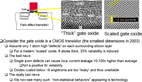
Classical scaling allowed one to produce a device burning exactly half the power of its predecessor, while reducing the area of the device by exactly a factor of two. This was absolutely critical, as it in ensured that a chip of fixed dimension, regardless of later generation, burned precisely the same power as the prior generation, despite having twice the number of devices in its area. This relied on precisely shrinking the dimensions of all elements of the transistor. However, in 2003, a critical element of the transistor, the gate oxide, reached a dimension at which its electrical behavior became dominated by a quantum mechanical phenomena known as tunneling.
Effectively, the previously insulating gate oxide layer had been rendered a useless conductor. This was the beginning of the end as to the performance benefits derived solely by scaling of the following generations of silicon technology. The impact is seen in Figures F-2 and F-3.
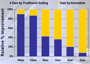
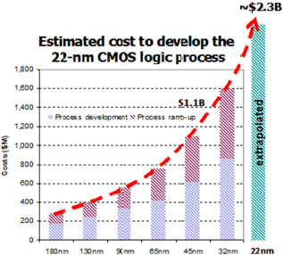
By virtue of the cost of the technological innovations required to mitigate such phenomena, this triggered the economic collapse of any subcritical scale commercial effort in silicon technology, resulting in a handful of leading-edge foundries surviving this transformation of the industry. With an inability to achieve material performance gains by the simple scaling of an existing silicon generation, the industry needed to resort to extremely costly innovations—in the materials used, the processing employed, device geometry, substrate materials, and a host of other elements—in producing the following generations. As represented in Figure F-3, this led to the rapid escalation in the cost of developing each subsequent generation of technology, similarly resulting in a rapid falloff in the number of vendors choosing to continue to pursue this strategy. The consolidation of this industry continues even today, and the complexity of the issues raised here has only become ever more problematic.
In recent technology generations, the benefits of next-generation technology for the actual performance of a single processing thread and/or core in a microprocessor have become essentially nil, as seen in Figure F-4. Compensating for this, more cores and other assets on a die have been implemented to improve performance at a system level (functionality/$), but in terms of raw performance from devices themselves, that benefit has gone asymptotically to zero.
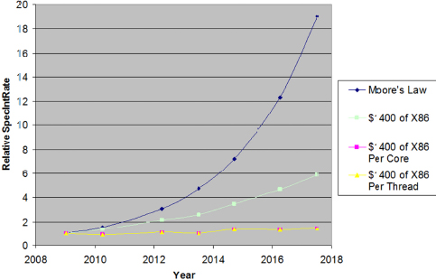
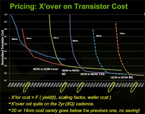
There are still clear benefits for power and performance and cost per function as represented by the increase in performance for a fixed dollar invested in X86 systems (see Figure F-5). However, to emphasize the implications of this long term, NVIDIA created the data in Figure F-5 from preliminary pricing and yield curves for past and future generations of silicon technology, as provided by NVIDIA, a fabless producer of graphics chips, and highlighted that over time, the drive to move to new generations goes away as future costs of manufacturing cause the cost per transistor for new generations to remain equal to or above that of prior generations (28 nm → 20 nm → 14 nm). This eliminates the key economic driver of movement to the next generation of technology, with implications as to the rate, pace, and economic success of this industry.
What is of concern is that for first time, the price per transistor of a following generation fails to fall below that of the prior generation, raising the issue of why one would move to the new generation given no improvement in the economics and little improvement in overall performance. It is not that there are no gains to be had, it is simply that they are asymptotically approaching zero.
With benefits of further scaling ever less with time, a more definitive statement can still be made. Silicon itself becomes the limiting material in the near term, at which time further scaling of any sort ceases to be viable. This is due to silicon itself being rendered un-usable when it approaches quantum mechanical limits at somewhere in the range of 4 to 7 nm. In this regime, even one or two atomic width deviations in device
dimensions will impart so much variability to devices as to make a circuit difficult, if not impossible, to produce in a controllable fashion. Compounding this problem, the metallization utilized for connectivity in such devices does not scale as well as silicon itself, also becoming a final gating factor. Therefore, it can be argued that it is unwise for the government to even consider an option under which it might acquire and operate a secure foundry at the very leading edge of technology. This is unwise from a technical, as well as financial, perspective. Such a leading-edge foundry could cost in excess of $10 billion to develop, and to be viable, it would have to be operated at virtually 100 percent utilization at all times. There is no volume at the leading edge of technology within the Department of Defense (DoD) or other agencies that would remotely fill even a small fraction of such a capacity, and the maintenance of such a facility at low-volume production is virtually impossible, should one want to ensure quality and process stability.
By contrast, back level foundries rapidly become legacy assets, so the government could expect to reasonably acquire such a relatively current (n-2,4) foundry for a dramatically discounted capital expense. However attractive this may seem, a full return on investments and return on assets analysis would be required to validate such an approach as sustainable. Although the initial capital expense would be minimized, the challenge remains in the overall operation and associated investment costs for such an endeavor. This comprehends everything from the creation of physical design kits, to the instantiation of a design flow, to the creation of what would effectively be a foundry support organization. This is not to presuppose success or failure of this analysis, but it is critical to comprehend what all associated costs will be upon the acquisition of the foundry in order to make such a judgment. Whereas previously one might dismiss this notion out of hand due to the rapid movement of silicon technology into the future, the asymptotic approach to silicon’s “end of life” in terms of further scaling greatly mitigates the rate at which such an asset would become such a legacy so as to burden its users.1 Having made these assertions to the point where further detailed analysis is required, it is also worth turning our attention to other means by which a secure supply line may be maintained without actually acquiring the large and ongoing challenges associated with semiconductor manufacturing.
As we enter this new era in terms of what drives system performance, new opportunities present themselves to mitigate supply chain risk. We are increasingly seeing the use of field-programmable gate arrays (FPGAs) and graphic processing units (GPUs) as accelerative elements within systems, rather than for the ready replacement of long lead time and design intensive application-specific integrated circuits (ASICs). It is significant that in realizing the importance of this emergent trend, Intel has acquired Altera, a leading FPGA manufacturer, and is implementing monolithic chips containing close-coupled CPUs and FPGAs having shared memory. Further, Xilinx has produced the next generation of system on module (SOM), which couples programmable logic with embedded ARM hard CPU cores. The availability of systems on a chip with a duality of functionality makes possible real-time monitoring and validation of critical FPGA functions by an independently programmed yet closely coupled CPU. It is likely, and seen from experience, that such functionally and architecturally diverse single chips can be more robust in terms of security of function than can be achieved with a simple software- or hardware-based defense. Active methods of real-time system assurance, whether by direct monitoring as elaborated here, or via behavioral monitoring as enabled by a cognitive system exploring departures from a norm, are options to be explored as first or second lines of defense against malicious functionality implemented in a critical system during its manufacture. Unfortunately, functionality running in so-called bare metal configurations runs at clock-rate speeds, whereas software does not. The implications are that real-time checking of hardware may be difficult to perform by software; however, hardware can be used to verify and validate correctness of software.
______________________
1 It may be that as silicon technology hits the end-of-life wall, there may ultimately be more suppliers who will be able to reach this capability limit in a cost effective way. Silicon fabrication will truly be a “commodity process” at this point, and not a differentiator on product performance.
This page intentionally left blank.


