
3
Assessment of LED and OLED Technologies
INTRODUCTION
The insertion of new solid-state lighting (SSL) technologies has caused a revolution in lighting over the past decade. During the 3 years following the first study, the lighting industry has undergone a fundamental restructuring, as detailed in other chapters of this report. It is possible to view this rapid change as proceeding in phases. According to this view, the first wave (dumb and “rudimentarily smart lighting” [Tsao et al., 2014]) has just been completed. This wave was dominated by retrofit into existing sockets and characterized by rapid increases in luminous efficacy. If there is to be a second wave (smart and feature-rich lighting), SSL technology will need new advances that encompass, beyond efficacy alone, the quality and form factors of lighting, their connectedness and controllability, and their cost-effective insertion into new applications.
This chapter discusses the key technological issues that still challenge light-emitting diode (LED) and organic light-emitting diode (OLED) technologies and that limit their high-efficiency performance. A basic understanding of the structure and, hence, operational principles of LEDs and OLEDs is important in setting the context of the technological challenges to be addressed and the possible new directions the lighting industry will take. Accordingly, the LED and OLED “primers” from the 2013 NRC report are also reprinted in the Chapter 3 Annexes 3.A and 3.B, “An LED Primer” and “An OLED Primer,” respectively. The primers treat the basic device structure and metrics of device performance.
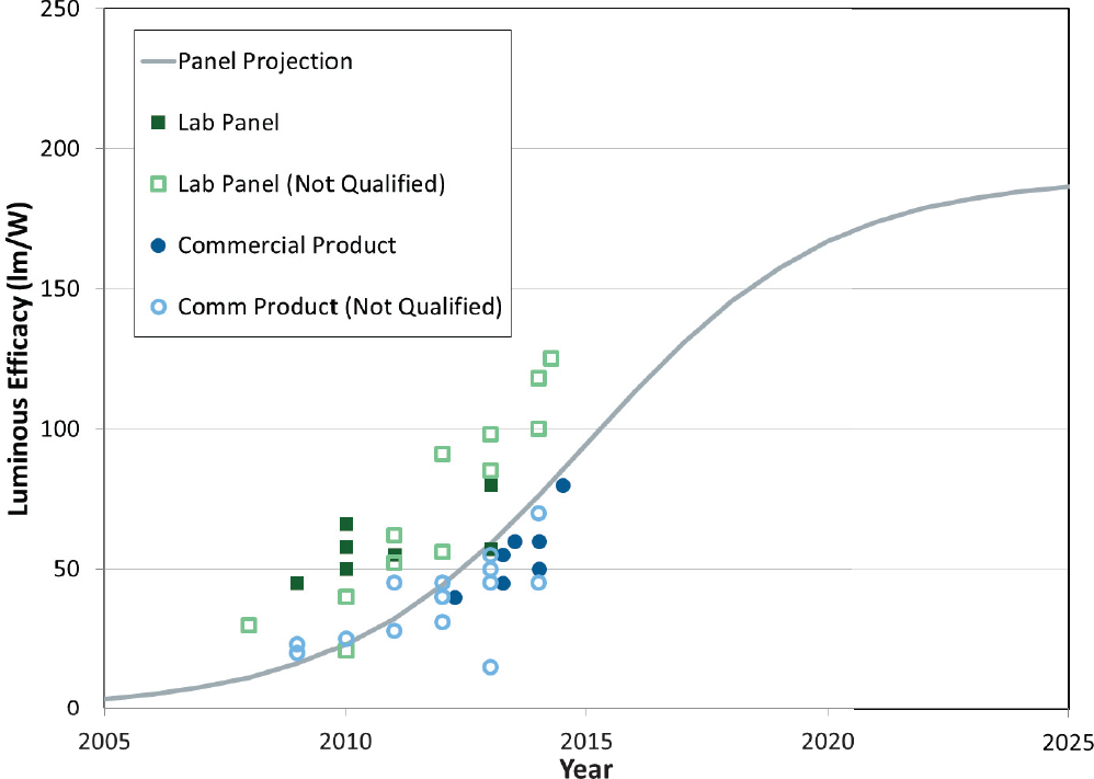
Figure 3.1 illustrates the recent progress made in lighting efficacy for both LEDs and OLEDs by examining the performance of different types of products on a yearly basis. Figure 3.1(a) distinguishes commercial LED packages with different LED architectures, showing current values of efficacy of 140 lumens per Watt (lm/W) for “warm white” lighting and 160 lm/W for “cool white” packages. Figure 3.1(b) displays the analogous projection in efficacies for OLED panels, based on data for both laboratory panels and commercial products.
There are a few clear observations we can make based on the data from Figure 3.1:
- There has been steady progress in increased efficacy of both LED packages and OLED panels. Yet for both LEDs and OLEDs, the projections suggest that still-higher efficacies are possible.
- While higher efficacies are possible for LEDs, the ultimate (saturation) values of efficacy differ and depend on the device physics of the package technology. These options include the following: (1) the current predominant architecture using phosphor-coated LEDs (pc-LEDs), with predicted saturation efficacy of 255 lm/W; (2) a “hybrid” technology LEDs (hy-LEDs) utilizing light emitted directly from LEDs together with light from pc-LEDs, for which the saturation efficacy is predicted to be 280 lm/W; and (3) the use of four separate LEDs (red, blue, green, and amber), where the saturation efficacy is predicted to be 330 lm/W. The predictions of different saturation efficacies for the different architectures indicate both the dominant mechanisms of efficiency loss today and the potential for improvements in the future.
- Data on commercial, qualified OLED panels remains sparse, and product performance in a given year is non-uniform, making future projections of progress all the more difficult. However, Figure 3.1(b) suggests that OLED panel efficacies of 190 lm/W are possible.
- LEDs and OLEDs for SSL remain at very different stages of development, and the critical challenges, and hence critical investments, for these technologies are expected to be different.
- As described in Chapter 2, DOE has provided research and development (R&D) support for SSL over a number of years and has published periodic roadmaps and R&D plans for the augmented capabilities of SSL. Current investments by DOE and the lighting industry in the core LED and OLED technologies have resulted in remarkable success; further investments are needed to consolidate the gains achieved in the first wave and pave the way for new, exciting, and perhaps unpredictable possibilities in the second wave. Yet for LEDs, the return on investment in developing energy savings alone appears to be getting much less attractive for industry. However, reduction in energy consumption is a key element of DOE’s mission. A greater understanding of the technological possibilities is needed to resolve these seemingly disparate objectives: on the one hand, the objective of (1) a continued singular focus on lumens per watt, which has been a focus of DOE, balanced against the objective of (2) development of new applications, capitalizing on increased light quality and integrated systems, for which the metric of lumens per watt is a secondary goal. This latter objective reflects the evolving industrial and market point of view. As industry is mindful of the cost of producing lighting systems, as well as lighting quality (based on customer demand), given the very competitive environment, industry is unlikely to on its own, fund higher-risk research aimed at improvements of lighting efficacy (lm/W).
Nonetheless, further technological solutions are necessary to deliver the maximum savings in energy for SSL. In addition, advances in core technology are necessary to implement the new generation of “smart,” feature-rich lighting applications, which require multicolor emission, narrowband emission spectra, and high modulation speeds.
KEY CORE TECHNOLOGY CHALLENGES FOR LEDS
There are four key performance factors to be considered in the evaluation of an LED package, and there are consequent trade-offs in the separate optimization of each of those performance factors. The trade-offs and ultimate efficiencies obtainable define the continuing challenges in improvements of the core technologies for LEDs.
- Drive current density determines the amount of luminous flux (light output) delivered to the LED package.
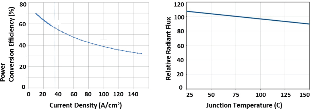
- Junction temperature refers to the local heating of the p-n junction, at the core of the LED operation (see Annex 3.A). As shown in Figure 3.2, both increased drive current density and increased junction temperature degrade the efficiency of LED output, by reducing the “power conversion efficiency” (Figure 3.2(a)), or the resulting light output (Figure 3.2(b)).1
___________________
1 The concepts of internal quantum efficiency (IQE) and external quantum efficiency (EQE) are introduced in Annex 3.A, “An LED Primer,” and Figure 3.4 demonstrates the droop or reduction in EQE as a function of current density in the LED. There are various ways of describing the efficient performance of an LED: Figure 3.7 uses power conversion efficiency, that is, the efficiency of conversion of electrical to optical power. Figure 3.8 uses the term wall-plug efficiency—another term that relates the applied electrical input power to the resulting optical output power. Although the exact numbers may differ, all of these terms are a metric of the efficiency of the power input to the LED (or laser) device or system, compared to the radiant power out.
- Correlated color temperature (CCT) has been more fully discussed in the section “Introduction to Lighting” in Chapter 1.
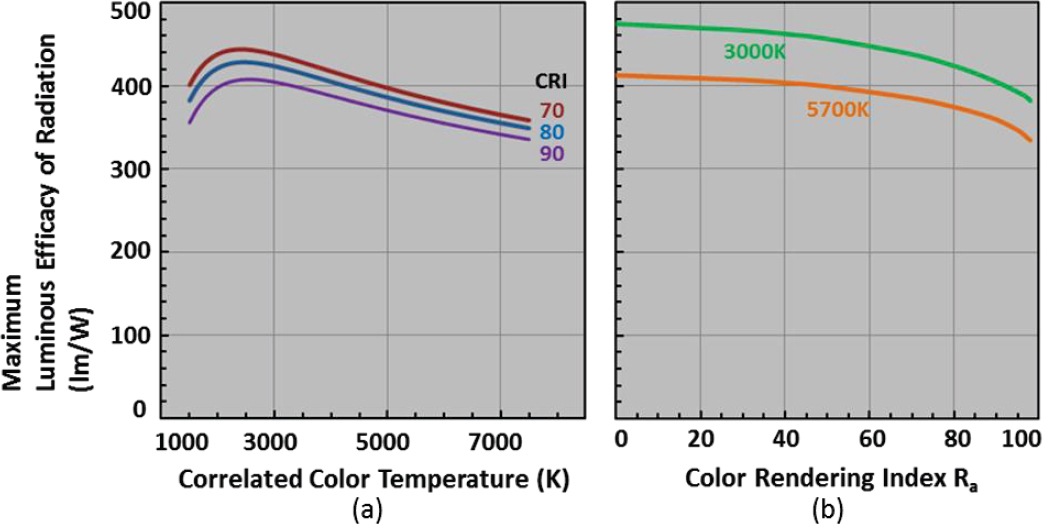
- Color rendering index (CRI) has also been more fully discussed, also in the section “Introduction to Lighting” in Chapter 1. The design of an LED package represents an engineering compromise between efficacy and light quality. There is an inverse relationship between the CRI and the efficacy, as shown in Figure 3.3.
Higher junction temperatures can lead to reduction of internal quantum efficiency (IQE) (see also Annex 3.A), increased device resistance, and other mechanisms that contribute to lowered efficiency. The data of Figure 3.2 illustrates a phenomenon commonly referred to as “droop” (reduction of light intensity). “Current droop” refers to decreased LED efficiency with increased applied current density, while “thermal droop” refers to the decreased efficiency with increased operational temperature of the device. Although high current densities can lead to higher junction temperatures, depending on the effectiveness of the LED packaging, the detailed physical mechanisms of current droop are distinctive from simple junction heating. These details are described in the section “Eliminating or Mitigating ‘Current Droop.’” Current droop has a particularly strong effect for LEDs emitting in the green and accentuates the low efficiency of LEDs at high current densities in this spectral region, giving rise to the phenomenon known as the “green gap.” This is discussed further in the section “Overcoming the ‘Green Gap.’” Thermal droop, in turn, has a particularly strong effect for red LEDs.
The core challenges for LED technology—droop, the green gap problem, and control over light quality—are all intimately related. Not surprisingly, droop is also an issue for OLEDs (although the physical basis for droop is different in these materials). While progress has been made in understanding and mitigating these issues, they still remain as fundamental challenges for the second wave of development.
Eliminating or Mitigating “Current Droop”
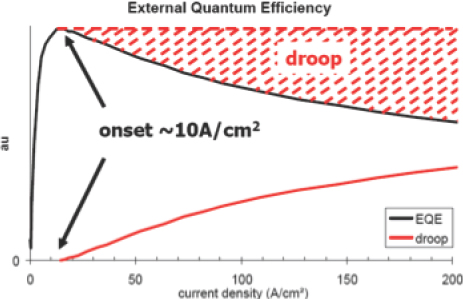
A continuing problem for the conventional III-nitride LEDs, which include, for example, gallium nitride (GaN), is the loss of efficiency under operation at high current densities (typically greater than 10 A/cm2). The phenomenon of “efficiency droop,” occurring at increased current densities, is illustrated in Figure 3.4. As the current density of the LED is increased, the external quantum efficiency (EQE, see Annex 3.A) is reduced. All commercial devices operate in some region of the droop curve, implying fundamentally reduced efficiency. The reduction of EQE at higher current densities has a profound effect on the economics of these LEDs. In the presence of droop, targeting a higher total light output in lumens now requires using multiple LED dies in a given area, each operating at lower current densities, rather than using a single LED in the same area that can be operated at a higher current density. Alternatively, lighting manufacturers might choose to use fewer LEDs, operating them at higher current densities but incurring the penalty of reduced efficiency. The impact on manufacturing costs is clear: there have been projections that a 6 percent improvement in droop could result in two or three times improvement in light output per dollar, for the same LED wall plug efficiency.2 The mechanisms associated with droop have also been linked to
___________________
2 E. Nelson, I. Wildeson, and P. Deb, Lumileds, presentation at the DOE Solid-State Lighting R&D Workshop in Raleigh, N.C., February 2-4, 2016.
the “green gap” problem (see the section “Overcoming the ‘Green Gap’”).
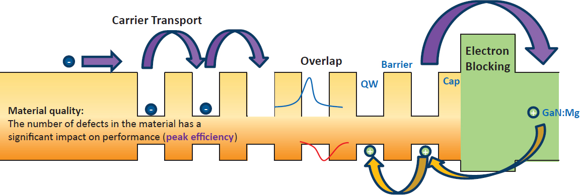
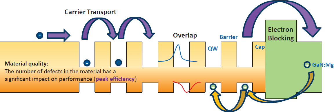
The root cause of droop is still subject to controversy, despite some recent very carefully executed and analyzed experiments.3 The key factors relate to the reduced internal quantum efficiency (IQE) (which is efficiency of the electron-hole conversion to photons) at high electron and hole concentrations (see Box 3.B.1 in Annex 3.B), and thus the mechanisms may relate to electron and hole “leakage,” the presence of a built-in electric field that reduces IQE, or mechanisms such as “Auger recombination.” This latter mechanism is particularly active under high current density: energetic electrons and holes in the LED recombine, but without the emission of light. Instead, the recombination energy is transferred to neighboring charge carriers and generates heat. It appears that there is a variety of interacting physical processes that take place in the active region of the LED: both electronic transport (the ease which electrons move through the device) and photon production efficiency need to be optimized, but often the improvement of one factor can only be done at the expense of the other. The situation is illustrated in Figure 3.5, which gives a schematic view of the multiple quantum well (MQW) regions in the LED, designed to facilitate radiative recombination of electrons and holes. MQWs are also discussed in Annex 3.A. The figure may allow easier visualization of the situation at high current densities, where the quantum well regions are “over-filled” with electrons or holes, the structure therefore becomes less effective in “holding” or localizing the electrons and holes, and the efficiency of light output is reduced.
A number of technical approaches hold promise for mitigating the effects of droop.
___________________
3 See, for example, Weisbuch et al. (2015).
- Creating “wider active areas” (quantum wells) and minimizing high carrier densities represents one approach. Growth on substrate materials other than sapphire might facilitate the wider active areas. For example, researchers and companies have explored the use of silicon carbide (SiC) as a substrate. This approach represents a compromise between reducing droop and increasing device resistance. Most recently, there has been some success with growth on GaN substrates (David, 2015). Further discussion on alternative substrate materials is given in the sections “Improved Epitaxial Growth and Substrates” and “The Manufacturing Supply Chain and Economic Drivers” in Chapter 5.
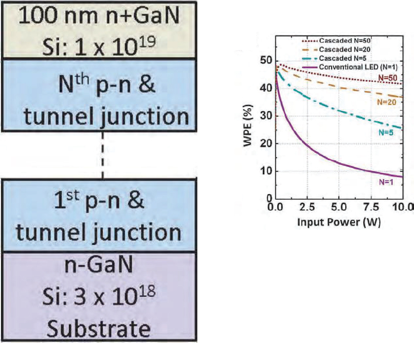
- Stacking LEDs (or their essential elements, the p-n junction) on top of each other allows increased voltage, but with low current density. The lower current density allows the device to operate at the high efficiency part of the droop curve (Figure 3.4). The end result is to produce higher light output per unit area of LED, while avoiding droop. The multiple “LEDs” or p-n junctions, as well as their connectors would be formed through epitaxial growth. A schematic of the stacked p-n junctions, and their simulated high power performance, compared with the performance of a single junction, is shown in Figure 3.6. Notice the projected increase in wall plug efficiency with an increased number of junctions. The challenge in this approach is the development of low resistance connections (tunnel junctions allowing quantum mechanical transport) between the various LEDs.
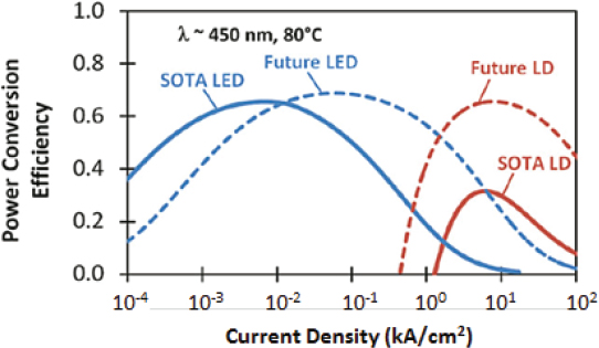
- Another solution that might side-step the limitations of efficiency droop is to employ a laser rather than an LED to pump a phosphor to create white light (Box 3.1). There are many similarities between a laser and an LED structure; however, the incorporation of a laser cavity to produce a nonlinear amplification of the light overcomes many of the limitations set by droop, and allows higher-efficiency operation at higher current densities. This is illustrated in Figure 3.7, which depicts the power conversion efficiency as a function of current density, for LEDs (both state-of-the-art and future devices), as well as laser diodes (LDs, also state-of-the-art and future devices). Both LEDs and LDs give off blue light (450 nm wavelength). While the power conversion efficiency of LEDs falls off, or droops, at current densities greater than ~ 10 A/cm2, current lasers reach their maximum values of power conversion efficiency at current densities as high as 1 kA/cm2. In fact, lasers have already been employed as white headlights in automobiles,4 and thus this technology is currently being implemented for commercial applications. However, Figure 3.7 also reveals some of the current limitations of using laser diodes for lighting applications:
- — The peak power conversion efficiency of blue lasers (about 30-40 percent) is lower than that of blue LEDs (about 80 percent).
- — Laser power conversion efficiency only applies after the laser threshold is exceeded (current thresholds are about 1 kA/cm2).
- — There is a reduction in power conversion efficiency for lasers operating at higher current densities, associated with electrical resistances in the device.
___________________
4 EVO, “BMW M4 shows off laser headlights with CES concept,” released January 8, 2015, http://www.evo.co.uk/bmw/m4/14912/bmw-m4shows-off-laser-headlights-with-ces-concept.
Lasers provide additional benefits as SSL sources: they possess narrow spectral linewidths (i.e., very precisely defined wavelengths) and high modulations speeds, enabling next-wave applications. However, the technological challenges are formidable in improving state-of-the-art blue lasers to achieve the power conversion efficiencies of future lasers, as indicated in Figure 3.7.
DOE has understandably made the reduction of droop an R&D priority5; the truly workable solution, however, is one that will be sufficiently cost-effective to induce adoption by lighting manufacturers.
Overcoming the “Green Gap”
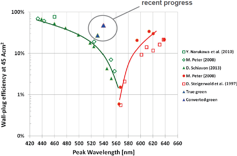
The loss of LED efficiency at higher current densities affects LEDs across the spectral range. The green gap is a manifestation of the efficiency droop discussed above, but affecting wavelengths in the green spectral region, and occurring at lower values of current density. The absence of high-efficiency LEDs in the green spectral range is particularly critical because the highest sensitivity of the human eye falls between 540 and 580 nanometers (nm) wavelength. Figure 3.8 illustrates the highest efficiencies achieved in LEDs as a function of wavelength: note that the green line refers to LEDs made from InGaN, while the red line refers to LEDs made from InGaAlP. (The InGaAlP is currently used to form red LEDs, and the reduced efficiency of LEDs at the “ideal” red wavelength of 614 nm (DOE, 2016) also has a limiting effect on the efficacy of white-light LED SSL; see the section “Control Over Color-Quality”). Differing approaches to mitigating the green gap include the following:
- A focus on altering the semiconductor structure itself may enhance the emission of light at a given current value. Researchers at Rensselaer Polytechnic Institute are attempting growth of the LED structure on alternative substrates,6 while researchers at OSRAM have shown the feasibility of an integrated green LED structure epitaxially grown atop of a blue LED structure: the blue LED “pumps” the green LED, leading to the output of green light.7
- Most commercial SSL products today employ phosphors pumped by LEDs to achieve desired colors (see the section “Control Over Color Quality”). Thus, one may use high-efficiency “green” phosphors pumped by blue LEDs.
___________________
5 “The Droop Phenomenon,” SSL Postings (postings@akoyanonline.com), March 30, 2016.
6 U.S. Department of Energy (DOE), “Solving the ‘Green Gap’ in LED Technology,” https://energy.gov/eere/ssl/solving-green-gap-led-technology, accessed March 7, 2017.
7 B. Hahn, op. cit.
- Still in the experimental, evaluation stage, solutions pursued by OSRAM have resulted in improvements in the wall plug efficiency in the green portion of the spectrum; these are shown as the blue triangles denoted as “recent progress” in Figure 3.8.
Control Over Color Quality
Metrics of color quality have been discussed in Chapter 1, and the next generation of “smart” lighting applications, employing multicolor emission with narrowband emission spectra, will likely require increased control of color quality. Color quality requirements may vary as a function of applications, as discussed in Chapter 4. From a device perspective, the color of the LED is determined by the composition and thicknesses of the quantum wells that make up the active layer. The manufacturing challenges lie in controlling composition and thickness of the quantum wells that produce the different LED wavelengths. There are different limitations to the IQE (see Annex 3.A) of the quantum wells associated with different wavelengths, resulting in the different wall plug efficiencies observed for red, green, and blue (RGB) LEDs, as has been discussed in the section “Overcoming the ‘Green Gap.’”
As described in the Introduction, there are different approaches or architectures used to produce packaged LED white lights.
- Phosphor-converted LEDs (pc-LEDs) are currently the dominant means of realizing LED-based white lighting. Pc-LEDs utilize a blue LED to pump phosphors that will emit at green and red wavelengths, thus producing white light. Pumping at blue wavelengths to produce light at longer wavelengths is a process known as “down-conversion.” The efficiency of the LED itself is folded in with the color-conversion efficiency of the phosphor to determine the total efficiency of the LED. A narrow band red phosphor can be added to improve the warmth of the resulting white light.
- Hybrid LEDs (hy-LEDs) use a blue LED to pump a green wavelength down-converter (phosphor); the blue and green light is subsequently mixed with light from a red LED to produce white light. Currently this approach is being pursued using red LEDs based on InAlGaP, and the limitations for the hybrid approach primarily relate to the efficiencies of the red LEDs,
- Red, green, blue, and amber (RGBA) color-mixed LEDs (cm-LEDs) are based on directly integrating four primary LEDs—blue, green, amber, and red—to produce white light. This approach has a number of advantages in achieving subtle tunings of chromaticity and luminaire efficacy of radiation (LER). However, the different efficiencies of LEDs at the various colors, together with differences in aging or response to high power or heat, compromise the color of the light source.
as shown in Figure 3.8. EQE of these LEDs are currently about 25 percent, and these LEDs are more greatly affected by thermal droop than InGaN-based blue LEDs.
Phosphors are available in a wide range of chromaticities for sensitive tuning of light quality; however, there continue to be challenges in the efficiency, thermal stability, and in the spectral width of these phosphors. Although the quantum yields for phosphors are currently quite high (98 percent for green, 90 percent for red), still further improvements are required, with DOE goals of 99 percent quantum yield for green and 95 percent for red, by 2020 (DOE, 2016). The thermal stability of the phosphors also are to be improved from the current value of 90 percent relative quantum yield at 125°C, compared to 25°C, to a target value of 95 percent by 2020 (DOE, 2016). In addition, a narrow spectral width of the phosphor is desirable, since a broad width near the red portion of the spectrum, as shown in the blue curve of Figure 3.9, can introduce an orange tinge to the color. Recent progress in narrow-spectral-width phosphors holds great
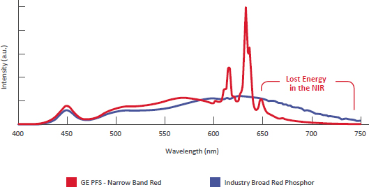
promise for future improvements in fine-tuning the color quality of LEDs.
It should be recognized that the phosphor-based approaches to achieving color quality may not adapt well to the demands of future smart solid-state LED lighting, which will require real-time tuning of light output to tailor white and non-white lighting chromaticity (Tsao et al., 2014).
Improved Epitaxial Growth and Substrates
The discussions above on efficiency droop and the green gap suggest that an important route for mitigation of these problems may require modified materials structures. These new structures will certainly require improvements in epitaxial growth and may use different substrates for that epitaxial growth.
Epitaxial growth is carried out through metal-organic chemical vapor deposition (MOCVD). The MOCVD deposition machines used in the manufacture of the LEDs have a huge influence on the uniformity of the wavelength and yield of white LED in a complicated process that requires control of temperature, material strength, and growth rates. There continue to be innovations and augmentations in the monitoring of the growth process: for example, DOE-funded research has helped to implement a Veeco MOCVD reactor with advanced wafer carrier design, near-ultraviolet pyrometry to monitor the temperature of the material during the growth, and utilizing a model-based means of temperature control.8 The resulting MaxBrightTM reactor claims improved wafer yields and wavelength uniformity.9
Epitaxial growth processes work best when the substrate (e.g., sapphire) that serves as the template for the material growth has a structure (lattice constant) that matches that of the finally formed material. Without the one-to-one registry of the overgrown material to the template, there will be a strain in the overlayer that may eventually give rise to dislocations and defects in the material (107-108 cm-2 dislocations in the best case for GaN on sapphire). Such defects will compromise the performance and reliability of the devices formed from the material. The proposed changes in device structure to reduce droop will place even more stringent requirements on MOCVD growth. Other challenges for epitaxial growth include developing new materials for green and red LEDs. These materials have large lattice mismatches to all commonly used substrates.
There have been some small advances in substrate availability since the 2013 NRC report. Sapphire (with an approximate 14 percent lattice mismatch) still has the largest share (95 percent of the market) as substrate material for LED growth.10 Although SiC provides a closer lattice match to GaN than does sapphire and appears to have some advantages over sapphire in GaN epitaxial growth, significant numbers of dislocations are still generated during the GaN epitaxy. As “a rule of thumb” large numbers of dislocations are generated when the substrate-to-epi lattice mismatch exceeds 1 percent (in the case of GaN/SiC the mismatch is ~3 percent). The semiconductor power electronics device market has provided an impetus for the development of SiC substrates, and SiC substrates have come down significantly in cost since the last report. Although SiC substrates are still much more expensive than sapphire, SiC substrates are now available as 6'' wafers with 8'' in development. Cree continues to provide GaN-on-SiC LEDs. GaN substrates would provide the closest lattice match to the LED structures, alleviating issues of materials of strain and compositional control during the growth. Laboratory results have already demonstrated superior efficiency at high current densities for LEDs grown on bulk GaN substrates (Hurni et al., 2015). However, this is still a relatively young technology and is challenged by issues of cost and substrate size. The production of GaN-on-GaN devices is being undertaken by SORAA and through funded research by DOE’s Advanced Research Projects Agency-Energy.11 Further discussion is given in the section “The Manufacturing Supply Chain and Economic Drivers.”
Challenges and Promises for LEDs
In recent years, there has continued to be substantial progress in achieving increased efficiency of LED-based lighting. Nevertheless, the fundamental challenges remain, relating to efficiency droop, green gap, and fine tuning of the color quality. There has been progress in the understanding of droop and the green gap, and some promising and innovative approaches have been demonstrated to mitigate these problems. Nevertheless, the adoption of these approaches and the consequent impact on SSL will inevitably be balanced against nearer-term costs as well as longer-term benefits.
FINDING: Major technological issues remain in improving the efficiency and performance of LEDs, including efficiency droop and the green gap in efficiency. Although there is a better understanding of the underlying mechanisms and possible solutions, including new approaches to lattice-mismatched epitaxy and the growth of LEDs on GaN substrates, the costs of implementing those solutions may be too expensive for industry to consider action. Laser sources, rather than LEDs for SSL, may mitigate some of the major challenges in droop and green gap, but these sources will
___________________
8 M. Pattison, “Led and OLED SSL Manufacturing Value Chain,” briefing January 5, 2016.
9 J. Jenson, Veeco, quoted in Jim Brodrick, DOE, “Briefing on DOE Solid-State Lighting Program,” presentation to the committee, November 11, 2015.
10 S. Pruitt, Strategies Unlimited, “Lighting and LEDs Market Overview and Forecast,” briefing January 5, 2016.
11 J. Brodrick, DOE, briefing to the committee on January 5, 2016.
require their own technological developments to realize low thresholds at low cost.
KEY CORE TECHNOLOGY CHALLENGES FOR OLEDS
There remains a great deal of interest in OLED-based lighting because of the diffuse quality of light (compared to LEDs as directional, “point-sources”) and the possibility of integration with flexible substrates, allowing a variety of form factors for OLED lighting.
As seen in Figure 3.10, progress has been made in the efficiency of OLED panels, with high potential anticipated for future improvements.12 The 2013 NRC report identified several key technology issues to be addressed for improved OLED performance. These issues included efficient light out-coupling, or extraction, as well as the relatively short lifetime of blue emitters compared to green and red emitters. These issues remain important limitations to OLED lighting efficacy. Nevertheless, in the intervening time, at the R&D level, the luminous efficacy has reached 135 lm/W, largely due to improvements in materials and the adoption of highly efficient light extraction schemes. On the production scale, today’s OLED panel efficacy is rated at 60 lm/W and manufacturers are promising 80 lm/W in next-generation products. Beyond the improvements in OLED efficacy, a conclusion of the 2013 NRC report was that there was as-yet not large-scale manufacture of OLEDs specifically installed for lighting, which is the root cause for the high price of OLED panels. This situation remains true today. Major growth in OLED display technologies could provide both incentive and leverage to the development of OLED lighting. Indeed, Active-Matrix Organic Light-Emitting Diode (AMOLED) displays for both mobile and TV applications form a rapidly growing business today, with estimated 2016 revenue of $15 billion.13 Planned installations of new G5 (Generation 5) to G8 (Generation 8) AMOLED manufacturing lines in Korea and China are expected to fuel further growth of OLED display business and accelerate price drops. The lowered cost of AMOLED displays, OLED-TV in particular, will directly benefit the OLED lighting business, since OLED
___________________
12 T. Komoda, China International OLED Summit, Shanghai, China, on January 21, 2015.
13 IDTechEx, “OLED Display Forecasts 2016-2026: The Rise of Plastic and Flexible Displays,” http://www.idtechex.com/research/reports/oled-displayforecasts-2016-2026-the-rise-of-plastic-and-flexible-displays-000477.asp, accessed August 23, 2016.
lighting shares a technology platform similar to OLED-TV: both are based on white OLEDs with a tandem (stacked) device architecture (described in Annex 3.B) and use mask-less vapor deposition for panel manufacturing.
FINDING: Because OLEDs for illumination and OLEDs for displays build on a common baseline of materials and devices, there is huge potential for improvements in the development of OLEDs for lighting by leveraging the infrastructure of OLEDs for displays.
Incipient Commercialization of OLED Lighting
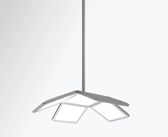
OLED lighting panels, both rigid and flexible and in various shapes and forms, are commercially available from a few manufacturers. The lead manufacturer is LG Display from Korea. The sole U.S. manufacturer is OLEDworks in Rochester, New York. The first generally available OLED lighting product in the United States is produced by Acuity Brands (the CHALINATM OLED pendant, Figure 3.11) and is currently sold in Home Depot as a specialty downlight.14 At a selling price of $299 per unit, the cost amounts to $3.75 per square inch of OLED panels. At 345 lumen total output the cost is $1,150 per kilo-lumen, which is at least two orders of magnitude higher than the cost of LEDs. However, in terms of luminaire pricing, the CHALINA OLED luminaire can be fairly competitive to similar specialty lighting products listed at Home Depot. OLED panels are also available from OLEDworks. According to its website, the average price (calculated for its model FL300) is approximately $3.15 per square inch, or $373 per kilo-lumen, not including the cost of the driver.
Increasingly, OLED panel manufacturers are offering flexible OLED lighting panels as unique and differentiating products. Figure 3.12 shows an example of such distinctive OLED lighting. Flexible products can be based on plastic (such as PET, polyethylene terephthalate) or ultra-thin glass (such as Corning’s Willow glass) substrates. Product specifications from LG indicate efficacy of 60 lm/W, similar to glass products, and L70 of 20,000 hours, about half of the glass products. The shorter L70 is likely due to encapsulation issues, which are generally more difficult to manage for flexible OLEDs. Higher moisture permeability in plastic materials and the lack of robust and cost-effective thin-film encapsulation methods are major issues in this case.
___________________
14 Home Depot, “Acuity Brands Chalina 5-Panel Brushed Nickel OLED Pendant,” http://www.homedepot.com/p/Acuity-Brands-Chalina-5-Panel-Brushed-Nickel-OLED-Pendant-CHALINA-PM-OLEDA1-5P-345LM-30K-120-DIM-B/205662976, accessed April 2016.
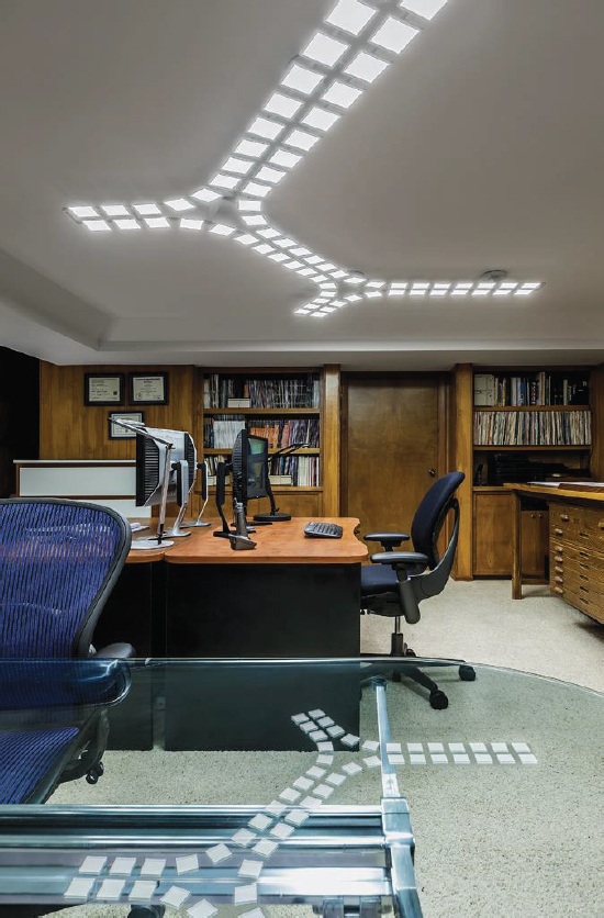
Furthermore, current adoption of OLEDs in luminaires, mostly in custom-design and specialty lighting applications, is limited due to the high cost of OLED panels and insufficient demand. Custom-installed OLED lighting demonstration products such as DOE’s Gateway Demonstrations (Figure 3.12) have been implemented to assess the viability of OLEDs as an alternative light source. A recently completely Gateway project (OLED lighting in the offices of Aurora Lighting Design, Ltd., March 2016) provides excellent light quality, eliciting comments from occupants such as “soft,” “inviting,” “desirable uniformity,” and “comfortable.” The project also revealed several performance issues, such as premature failure of some OLED panels due to electrical short, drive incompatibility, and related flickering—evidence that the OLED lighting industry is still in its early stages. The high cost of OLED panels remains the key hurdle encountered in OLED lighting business today.
Lifetime Issues
Achieving long shelf lifetimes requires assurance that the encapsulation scheme is sufficiently robust. This problem has been adequately solved for OLED displays, and approaches used for displays are expected to be of value for OLED SSL. Encapsulation approaches used in manufacturing include (1) glass to glass hermetic seals, (2) incorporation of desiccants inside the display panel, (3) thin-film encapsulation including atomic layer epitaxy (ALE), and (4) alternating soft/hard multilayered overcoat. The adoption of a specific approach for the thinner panels of OLED lighting will be cost driven.
Achieving a long operating lifetime principally relies upon a reduced current density through the OLED device, with a consequent reduction of electrochemical reactions (exciton-polaron interactions). The key means of reducing current density include (1) increasing the electroluminescence efficiency through molecular design and careful optimization of the device architecture; (2) improvement in light out-coupling efficiency, including the use of both internal and external light extraction layers, and preferred chromophore orientation; and (3) implementation of tandem device structures with multiple emitter units.
The short lifetime of blue emitters relative to green and red emitters is a major performance issue for OLED SSL products. Green and red emitters based on phosphorescent materials are commonly used in today’s OLED display and SSL products; however, there is a lack of blue phosphorescent emitters that have sufficiently long lifetimes. Therefore, fluorescent emitters are used in the blue spectral range, which are not as efficient as phosphorescent emitters (see Box 3.B.1 in Annex 3.B). This limits the overall OLED luminous efficiency. For OLED SSL, the color balance between blue, green, and red emitters that is needed to produce white light of a specific color temperature is achieved by utilizing a tandem structure (see Annex 3.B). This incorporates a blue fluorescent OLED stacked with a phosphorescent yellow OLED, emitting both green and red. By this means, the lifetime of white OLEDs has been significantly improved, and OLED SSL product lifetime (L70) rated at 40,000 hours has been produced for rigid OLED product panels at an initial surface brightness of 3,000 cd/m2 or equivalent light output of 9,425 lm/m2. L95 of 5,000 hours at similar light output has been measured.
Manipulation of the tandem structure to include more than one blue stack provides a pathway to further improve the lifetime of the white OLED, and this also allows shifting the white spectrum to a higher color temperature. However, the lack of stable phosphorescent emitters has placed a limit of only about 40-60 lm/W on the luminous efficacy of these current OLED SSL products.
Best Research Results for OLED Lighting Panels
Achieving power efficient white OLEDs requires high internal quantum efficiency, low operating voltage, and high light out-coupling (extraction) efficiency. While internal quantum efficiencies in OLEDs have already approached 100 percent (Uoyama et al., 1998; Wang and Ma, 2010; Baldo et al., 1998), light out-coupling, which can be as low as 20 percent in conventional OLED structures, remains a primary challenge. The examples below show some recent, excellent performance in both efficacy and light-extraction from the R&D sector.
OLED lighting has achieved an efficacy of 133 lm/W in laboratory panels (10 cm × 10 cm) from Panasonic, 97 lm/W in development panels (10 cm × 10 cm) from LG, and 40 to 60 lm/W in product panels (up to 300 cm × 300 cm) from LG and other vendors. It should be noted that because the OLED is a diffuse surface emitter, the brightness of the surface is independent of the viewing angle, and the efficacy measured for an OLED “bulb” or panel may be or may not be equivalent to luminaire efficacy, depending on the luminaire design. Some further descriptions of those panel results are given below.
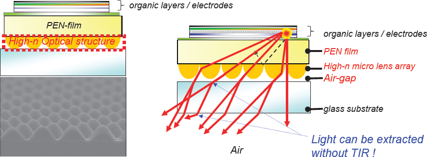
Panasonic has employed a novel high-index-of-refraction (n = 1.8) substrate together with high-index microstructure to carry out the light-outcoupling. A schematic of the device is shown in Figure 3.13 (Yamae et al., 2014). The panel incorporates all phosphorescent RGB emitters and operates with the highest reported values of EQE (56 percent per unit), as well as the highest efficacy reported, 133 lm/W for a large (10 cm × 10 cm) panel. The estimated L50 is greater than 150,000 hours.
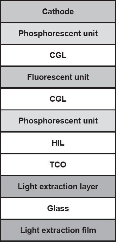
LG’s panel incorporates a hybrid design with fluorescent (blue) and phosphorescent (red and green) emitters, a dual extraction layer: one internal and one external (Jang et al., 2015) A pixelated anode (1 mm2/pixel) helps to eliminate electrical shorts and panel failures. The efficacy of this panel was 97 lm/W, with a measured L95 of 4,200 hours and a projected L70 of 40,000 hours. A schematic of the OLED structure is shown in Figure 3.14.
Novel Approaches to Enhanced OLED Performance
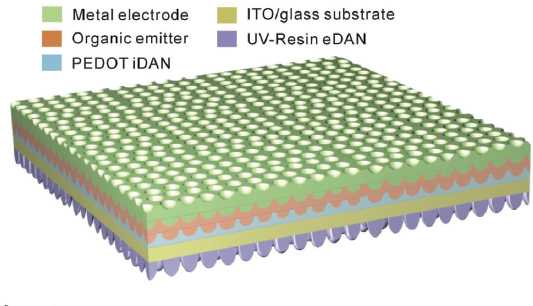
The research community has also found approaches that quite naturally incorporate light out-coupling structures into the OLEDs. As shown in Figure 3.15, incorporation of nanostructures using soft-lithographic nano-printing for both internal and external light extraction in an OLED device has resulted in 54.6 percent EQE with 123.4 lm/W at 1,000 cd/m2 (Ou et al., 2014). Other work has shown the benefits of aligning the molecular emitters for enhanced outcoupling of light through the substrate, resulting in improvements in external quantum efficiency (Kim et al., 2013). Consequently, new emitters have been developed, including blue hosts and dopants with molecular geometries that favor horizontal alignment (Kuma and Hosokawa, 2014).
FINDING: Major technological issues remain in improving the efficiency and performance of OLEDs, including efficient light extraction and reduced lifetime in the blue emitters. There is enough basic understanding of these issues to make progress in these areas. Some of the considered solutions have an important dependence on future manufacturing choices.
Challenges and Promises for OLEDs
Excellent progress has been made in achieving high OLED efficacy and long operational lifetimes in OLED panels for lighting applications. OLED panels as large as 320 cm × 320 cm are commercially available, with a tandem device structure and an integrated light extraction layer. These panels are rated at 60 lm/W and 40,000 hours. Efficacy as high as 133 lm/W has been demonstrated in the laboratory with further improvements in the light extraction scheme. Thin and lightweight OLED panels on plastic substrates with performance to OLED on glass are being produced,
thus offering a new opportunity in the design of luminaires. However, the cost of OLED panels today remains too high (relative to LED products) to be a viable solution for general lighting applications. Current OLED panels are primarily used for decorative or specialty luminaires where the cost is determined by the luminaire’s design or unique features (thin, light, curvy, transparent), rather than practical utility. As such, the adoption of OLEDs for lighting has so far been minimal and will remain so until the cost of manufacturing OLED panels is significantly reduced. The long-term viability of OLEDs for SSL can only be established after the critical issues of manufacturing have been confronted and assessed.
FINDING: The luminous efficacy achieved in OLED lighting products is in the range of 40-60 lm/W, which is about a factor of two below that of general LED lighting products. This makes current OLED lighting products uncompetitive for general lighting applications.
SUMMARY AND COMPARISON OF LED AND OLED SSLS
Since the 2013 NRC report, LED and OLED SSL technologies have made substantial progress in demonstrated efficacies. Indeed, the widespread insertion of LED-based SSL has catalyzed a wealth of new lighting-based applications, as well as demands for higher quality of lighting. The development of OLED manufacturing for display technologies can provide substantial leverage for progress in the materials and performance of OLEDs for lighting, and there has been progress in providing commercially available OLED panels for lighting, with high efficacy and long operational lifetimes. However, the costs of such panels are substantially higher than for LED SSL counterparts (Table 3.1), and the adoption of OLEDs for lighting has thus far been minimal.
Although there has been tremendous progress in the core technologies of both LEDs and OLEDs, many of the fundamental technological challenges are still dominant today (e.g., LED droop at high current densities, unequal efficiencies for different LED wavelengths, light extraction efficiency for OLEDs). In the case of LEDs, a highly competitive market promotes “working around” the technological challenges where possible (e.g., operating multiple LEDs at lower current densities to avoid droop). In the case of OLEDs, the costs of a manufacturable technology severely limit the current demand for OLEDs in SSL.
It is imperative that investments continue to be made in addressing and ameliorating the core technological challenges; indeed, these improvements will be even more critical for SSL to meet the second wave demands of smart, ultra-efficient SSL.
FINDING: Major technological issues remain to improve SSL efficiency, in both LEDs and OLEDs. Although there is a better understanding of the underlying mechanisms and possible solutions, the costs of implementing those solutions may be too expensive for industry to consider action. DOE has wisely focused on R&D priorities for core technologies that address the key technological challenges for high-efficiency SSL. These investments are critical.
TABLE 3.1 Comparison of Lighting Sources by Various Metrics
| Fluorescent | LEDs | OLEDs | |
|---|---|---|---|
| Efficacy (laboratory demo) | 231 lm/W (cold white) 150 lm/W (warm white) | 133 lm/W | |
| Efficacy (commercial) | 90 lm/W | 100-120 lm/W (white) | 65 lm/W (warm white) |
| Color rendering index | 80-85 | 85 (white) 95 (warm white) | Up to 95 |
| Form factor | Long or compact gas-filled glass tube | Point source high-intensity lamp | Diffuse source, thin, lightweight, transparent, flexible |
| Lifetime (hours) | 20,000 | 50,000 | 40,000@3000 cd/m2 |
| Cost ($/klm) | 1.0 | 3.0 | 100-250 |
NOTE: LED = light-emitting diode; OLED = organic light-emitting diode.
RECOMMENDATION 3-1: The Department of Energy should continue to make investments in core technology improvements for solid-state lighting technologies, both light-emitting diodes and organic light-emitting diodes, and should also consider solutions that will ultimately allow low-cost implementation and embody risks that industry is not likely to take. Early-stage investment in disruptive technologies represents high risks that industry is not likely to take.
REFERENCES
Baldo, M.A., D.F. O’Brien, Y. You, A. Shoustikov, S. Sibley, M.E. Thompson, and S.R. Forrest. 1998. Highly efficient phosphorescent emission from organic electroluminescent devices. Nature 395:151.
David, A. 2015. “Top Ten Challenges for Solid-State Lighting #9-Brightness.” March 13. http://www.soraa.com/blog_entries/38.
DOE (U.S. Department of Energy). 2016. Solid-State Lighting R&D Plan. DOE/EE-1418. Washington, D.C. May.
Hurni, C.A., A. David, M.J. Cich, R.I. Aldaz, B. Ellis, K. Huang, A. Tyagi, R. DeLille, M.D. Craven, F.M. Steranka, and M.R. Krames. 2015. Bulk GaN flip-chip violet light-emitting diodes with optimized efficiency for high-power operation. Applied Physics Letters 106:031101.
Jang, S.,Y. Lee, and M.C. Park. 2015. OLED lighting for general lighting applications. SID Symposium Digest of Technical Papers 46(1):661-663.
Kim, S.-Y., W.-I. Jeong, C. Mayr, Y.-S. Park, K.-H. Kim, J.-H. Lee, C.-K. Moon, W. Brütting, and J.-J. Kim. 2013. Organic light-emitting diodes with 30% external quantum efficiency based on a horizontally oriented emitter. Advanced Functional Materials 23(31):3896-3900.
Kuma, H., and C. Hosokawa. 2014. Blue fluorescent OLED materials and their application for high-performance devices. Science and Technology of Advanced Materials 15(3):034201.
Ou, Q.-D., L. Zhou, Y.-Q. Li, S. Shen, J.-D. Chen, C. Li, Q.-K. Wang, S.-T. Lee, and J.-X. Tang. 2014. Extremely efficient white organic light-emitting diodes for general lighting. Advanced Functional Materials 24(46):7249-7256.
Tsao, J., M. Crawford, M. Coltrin, A. Fischer, D. Koleske, G. Subramania, G.T. Wang, J.J. Wierer, and R.F. Karlicek, Jr. 2014. Toward smart and ultra-efficient solid-state lighting. Advanced Optical Materials 2(9):809-836.
Uoyama, H., K. Goushi, K. Shizu, H. Nomura, and C. Adachi. 2012. Highly efficient organic light-emitting diodes from delayed fluorescence. Nature 492:234-238.
Wang, Q., and D. Ma. 2010. Management of charges and excitons for high-performance white organic light-emitting diodes. Chemical Society Reviews 39: 2387.
Weisbuch, C., M. Piccardo, L. Martinelli, J. Iveland, J. Peretti, and J.S. Speck. 2015. The efficiency challenge of nitride light-emitting diodes for lighting. Physica Status Solidi 212:899-913.
Wierer, J., and J. Tsao. 2015. Advantages of III-nitride laser diodes in solidstate lighting. Physica Status Solidi A 212(5):980-985.
Yamae, K., V. Kittichungchit, N. Ide, M. Ota, and T. Komoda. 2014. Distinguished paper: Realization of outstandingly high efficacy white OLED by controlling evanescent mode and wide angular incident light. SID 2014 Digest 45(1):682-685.
ANNEX 3.A AN LED PRIMER
Introduction
Semiconductor light emitting diodes (LEDs) are a special kind of electronic device, which emit light upon the application of a voltage across the device. Silicon (Si) is probably the best-known semiconductor material, and the basis of the integrated circuits that underlie the fast and compact electronic devices, such as computers and cell phones, that are so critical to our daily lives. LEDs are based on a semiconductor material comprised of several different elements. This material is known as a compound semiconductor. The tremendous power of semiconductors lies in their ability to take on a wide range of conductivities, from metallic to insulator. This is brought about by “doping” the semiconductor with other elements that will donate either positively or negatively charged carriers to achieve a desired conductivity.
Semiconductors can also absorb and emit light, and the relevant wavelengths are related to the bandgap of the semiconductor (see Box 3.A.1). The general process for light emitted in this manner is referred to as electroluminescence. The first high-efficiency light-emitting devices were developed in the 1960s utilizing gallium arsenide (GaAs), aluminum gallium arsenide (AlxGa1xAs), gallium phosphide (GaP) and gallium arsenide phosphide (GaAsxP1-x) (Hall et al., 1962; Nathan et al., 1962; Pankove and Massoulie, 1962; Woodall et al., 1972; Herzog et al., 1969). GaAs and AlGaAs LEDs produced light with infrared wavelengths, ~850 nanometers (nm), while the gallium phosphide-based LEDs produced light in the red and green wavelengths. In the early 1990s efficient blue LEDs based on III-nitride materials began to appear based on the work of Akasaki et al. (1992) and Nakamura et al. (1994). (The III refers to elements in the third column of the periodic table, indicating that these LEDs can be comprised of alloys of aluminum nitride (AlN), gallium nitride (GaN) and indium nitride (InN)). The bandgaps of these III-nitrides produce light emission across a range of wavelengths spanning the infrared to ultraviolet parts of the spectrum. The III-nitride LEDs have had an unusually rapid development and huge impact on appearance of SSL. Although the first GaN LED was reported by Pankove et al. (1971), almost two decades transpired before substantial further progress was made by Akasaki and Nakamura. Amano and Akasaki demonstrated that high crystal quality GaN could be grown by MOCVD using a novel low-temperature buffer (Amano et al., 1986) and later succeeded in using electron beams to activate Mg receptors (Amano et al., 1989). In 1992, Nakamura, working at Nichia, developed an industrially robust process for p-doping of GaN that led to the first high-brightness blue LEDs. This provided the understanding of the mechanisms that had limited the conductivity of p type material and allowed for the first time the fabrication of low-voltage p-n junction LEDs and eventually led to the commercialization of high-brightness blue and white LEDs for SSL. The wider bandgaps of the III-nitrides enabled efficient LEDs emitting light at blue wavelengths, which together with green and red LEDs provided the basis for white light as well as full-color displays. The nitride blue emitters can also be coupled with phosphors to generate white light, which is currently the dominant approach to an SSL technology. The later introduction of blue LEDs, compared to their green and red counterparts, is the result of materials issues that are still of importance today: the lack of a well-matched material (substrate) upon which to form the LED structures, and some difficulties in controlling the electrical properties of the material. Nonetheless, the III-nitride materials have been pivotal in the success of inorganic SSL, and thus the committee will focus here on LEDs formed from those materials. There are several good reviews of LED device technology (see, for example, Schubert (2006) as well as III-nitride materials technology in Pankove and Moustakas (1998).
The LED Device Structure
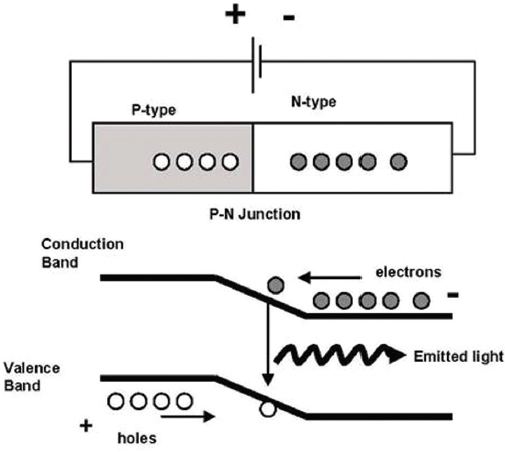
The basis of the LED device is a p-n junction diode, shown schematically in Figure 3.A.1. As the name implies, there is a junction between the N-type material (rich in electrons) and P-type material (rich in holes). Under forward bias (positive voltage applied to the P-region and negative voltage applied to the N region) large numbers of electrons are injected into the N region and large numbers of holes are injected into the P region.
Current flows in the device and the large number of injected electrons and holes can combine radiatively, producing significant light emission. The basic structure is modified in actual LEDs to (1) improve the efficiency of injection of electrons and holes and to (2) “localize” the electrons and holes and improve the likelihood of radiative recombination. This localization is accomplished by introducing multiple quantum wells (MQWs) in the region of the junction: the MQWs are indicated in the inset of Figure 3.A.1. These are thin slivers of lower bandgap-materials that, as their name implies, serve as wells that confine pools of electrons and holes to increase the probability that they will recombine radiatively. The multiplicity of the quantum wells ensures greater light output. Figure 3.A.2 provides some more detail of the multiple quantum well structures. Now electrons injected into the N region, and holes injected into the P region can be localized within the quantum wells until they recombine to emit light. Figure 3.A.2 also suggests that under conditions of high current injection (a large density of electrons and holes), the quantum wells may completely fill up, localization no longer takes place, and radiative recombination, or the emission of light, becomes inefficient. The over-filling of the quantum wells is related to the problems of droop at high current densities.
The external view of the typical LED structure is given in Figure 3.A.3, showing the N-type GaN, the InGaN quantum wells, and the P-type GaN. Most GaN LED devices are formed on a sapphire substrate through a process termed Metal Organic Chemical Vapor Deposition (MOCVD). Typically, one 4-inch diameter sapphire wafer can produce 5,000 individual devices or “dies.” The 16 percent mismatch in natural lattice size between the sapphire substrate and
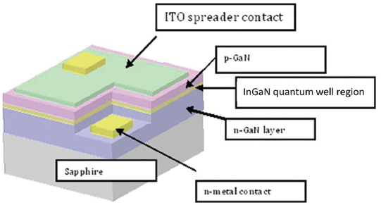
the GaN overlayers has important consequences on device performance and on the uniformity of the dies grown from a single wafer. In order to connect the device to the outside world, metal contacts must be deposited by evaporation on the N and P regions. Figure 3.A.3 shows these metal contacts, as well as the transparent and conductive indium tin oxide (ITO) layer that extends the top-side electrical contact over the device surface. Both the sapphire substrate and the ITO spreader contact are transparent to the emitted light, as is necessary for the light to leave the device. High-quality electrical contacts are important to reduce loss due to resistance (R) to current flow (I) in the contact region. This is even more important when the device is operated at high currents or current densities, since loss of power due to resistive heating scales as I2R. In the III-nitride materials, it is a challenge to dope the materials to a sufficient level so that resistances are low, particularly for P-type materials. The formation of the device structure shown in Figure 3.A.3 is just a starting point for the fabrication of the final solid-state “light bulb.” An individual device must be further “packaged,” as shown in Figure 3.A.4, to better control its chemical, thermal and electrical environment and to better integrate it into the final luminaire.
The LED Module
The LED package is the structure in which the LED chip is mounted and through which access to the LED terminals is provided. It is an important part of the finished device. The package serves many functions: (1) the package passivates or protects the active semiconductor material from degradation due to the environment (principally moisture); (2) the package integrates an optical lens structure which determines the optical emission pattern of the structure; (3) the package removes heat from the device, protecting against degradation due to overheating; (4) the package protects the device from Electro Static Discharge (ESD) failure. The packaging processes include placement of the device in the chip carriers, attachment of the optical lens, as well as electrical and optical device testing and “binning.” Because of the variability in the color accuracy, color quality and color stability, each device must be individually tested and placed in performance bins. In addition, if phosphor coatings are used in connection with the LED to control the output color, the phosphor must be added to the device or package.
A schematic of a typical LED package is shown in Figure 3.A.4. A major element of the package is the lens/ encapsulate assembly. The lens is integrated with a polymer encapsulation material which entirely encloses the chip. The plastic lenses/encapsulate material must have the required optical properties for light focusing as well be able to with-
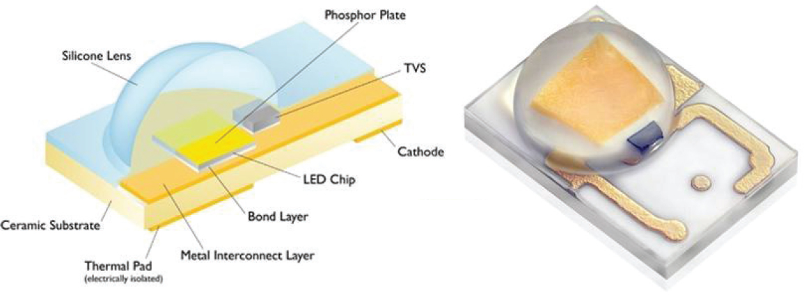
stand constant optical radiation and elevated operating temperatures without loss of transparency. The LED semiconductor chip or “die” is attached to a reflector cup (not shown explicitly in the Figure 3.A.4) which redirects all light to the plastic lens structure. The LED is attached to the reflector cup with a conductive epoxy. This process step is called die attachment. The conductive epoxy is usually loaded with silver (Ag) in order to increase the optical reflection. The reflector cup also contains the phosphor material, which is used to generate the additional wavelengths required for white light production. The package base produces two leads, which connect the LED to the outside world. Typically one package lead is integrated with the base of the package. The base of the package in turn is connected via conducting materials and conductive epoxy to one side of the LED die. The opposite side of the LED die is connected to the cathode by a second electrically isolated gold bond wire. The “silicon submount” structure shown in the figures incorporates devices that limit the build-up of static charge (“static electricity”) which could destroy the LED. The submount structure is attached to a copper slug, which serves as an efficient heat sink, preventing the loss of efficiency that occurs at very high temperature operation. This is necessary to maintain device reliability.
Metrics of Device Performance
Efficiency is an important metric of LED device performance, and some insights into efficient operation can be gained by tracing the life-cycle of the LED operation beginning with the injection of electrons and holes, shown in Figure 3.A.2, leading to the generation of photons within the device, and culminating with the emission (or extraction) of the photons from the device. A simple summary of the total external quantum efficiency (EQE, or ηEQE) of an LED can be expressed as
ηEQE = ηIQE • ηout
where ηIQE is the internal quantum efficiency (IQE), and ηout is the outcoupling efficiency, which is discussed below.
Internal Quantum Efficiency
Not all electrons and holes that are injected into the LED (e.g., from a battery) will produce photons: for example, defects in the LED material can trap an electron or a hole, and prevent the formation of a photon. The percentage of photons generated, relative to current (of electrons or holes) that is injected into the device is reflected in the IQE. ηIQE can be maximized by using quantum well structures as described above, by utilizing defect-free semiconductor material, and by ensuring high-quality, very low resistance metal contacts to the device. ηIQE also sensitively depends on the quality of the LED material. Because the quantum well composition and strain varies with the desired emission wavelength, ηIQE varies with wavelength. At present, there are still large differences in the power conversion efficiencies of blue (66 percent), green (22 percent) and red (44 percent) LEDs (DOE, 2016, p. 145), equal efficiency of LEDs at all colors is important, and further improvements towards 100 percent ηQE will require far better control of the material defects.
Current and Thermal Droop
As described in the section “Key Core Technology Challenges for LEDs,” two of the most important issues holding back efficiency at high illumination levels is the droop in efficiency as the LEDs is driven at higher currents and the effect of temperature. These issues are known in the industry as “current droop” and “thermal droop.” A fuller discussion of these factors is also given in “Key Core Technology Challenges for LEDs.”
Outcoupling Efficiency
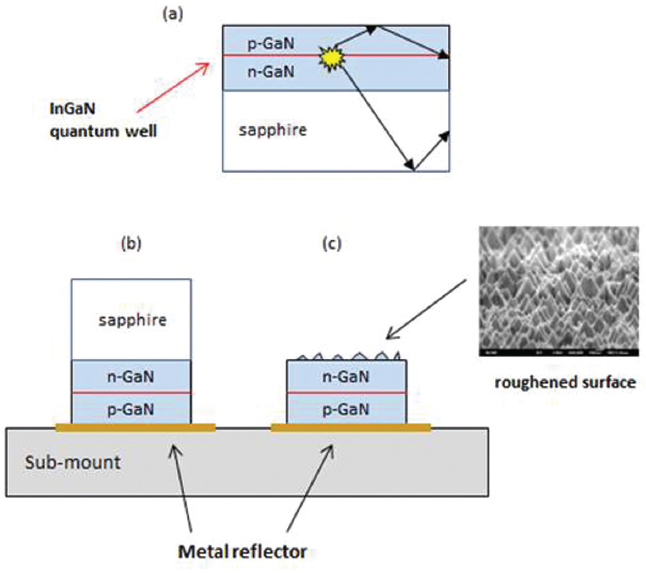
Once the photons have been formed in the LED structure, care must be taken to ensure that they will exit the device. The ratio of photons leaving the device to the number generated within the device is called the outcoupling efficiency, or light extraction efficiency. Because the LED material has a higher index of refraction (n ~ 2.5) than air (n = 1), most photons incident on the GaN-air interface will be internally reflected and trapped within the LED structure or absorbed (lost) by other materials comprising the device (see Figure 3.A.5). A thin metal film can serve as a mirror to direct the light out through the “front surface” of the LED. The internal reflection and trapping of the light can be mitigated by forming a rough, rather than smooth top LED surface; one way of achieving this is through the immersion of the device structure in a simple wet chemical etchant (Fujii et al., 2004). Such techniques can improve the extraction efficiency from a few percent to values of 80 percent (Krames et al., 2007).
External Power Efficiency
Finally, the external power efficiency (ηP) is defined as the ratio of the total optical power output of the LED to the electrical power input. Low resistive power loss, high ηIQE, and good design to maximize ηout produce high power efficiency in LEDs. Maximizing the power efficiency not only increases the efficacy of the LED but also reduces the heat removal problem.
References for Annex 3.A
Akasaki, I., H. Amano, K. Itoh, N. Koide, and K. Manabe. 1992. GaN-based ultraviolet/blue light-emitting devices. Institute of Physics Conference Series 129:851-856.
Amano, H., N. Sawaki, I. Akasaki, and Y. Toyoda. 1986. Metalorganic vapor-phase epitaxial-growth of a high quality GaN film. Applied Physics Letters 48(5):353-355.
Amano, H., M. Kito, K. Hiramatsu, and I. Akasaki. 1989. P-type conduction in Mg-doped GaN treated with low-energy electron-beam irradiation (Leebi) [in English]. Japanese Journal of Applied Physics Part 2-Letters 28(12):L2112-L14.
DOE (U.S. Department of Energy). 2016. Solid-State Lighting R&D Plan. DOE/EE-1418. Washington, D.C. May.
Fujii, T., Y. Gao, R. Sharma, E.L. Hu, S.P. DenBaars, and S. Nakamura. 2004. Increase in the extraction efficiency of GaN-based light-emitting diodes via surface roughening. Applied Physics Letters 84(6):855-857.
Hall, R.N., G.E. Fenner, J.D. Kingley, T.J. Soltys, and R.O. Carlson. 1962. Coherent light emission from GaAs junctions. Physics Review Letters 9:366.
Herzog, A.H., W.O. Groves, and M.G. Craford. 1969. Electroluminescence of diffused GaAs1-xPx diodes with low donor concentrations. Journal of Applied Physics 40:1830.
Krames, M.R., O.B. Shchekin, R. Mueller-Mach, G.O. Mueller, L. Zhou, G. Harbers, and M.G. Craford. 2007. Status and future of high-power light-emitting diodes for solid-state lighting. [in English]. Journal of Display Technology 3(2):160-175.
Nakamura, S., T. Mukai, and M. Senoh. 1994. Candela-class high-brightness InGaN/AlGaN double-heterostructure blue-light-emitting diodes. Applied Physics Letters 64:1687.
Nathan, M.I., W.P. Dumke, G. Burns, F.H. Dill Jr., and G.J. Lasher. 1962. Stimulated emission of radiation from GaAs P-N junctions. Applied Physics Letters 1(3):62-64.
Pankove, J. ., and M.J. Massoulie. 1962. Injection luminescence from GaAs. Bulletin of the American Physical Society 7:88.
Pankove, J. I., and T. D. Moustakas. 1998. Gallium Nitride (GaN) I. Semiconductors and Semimetal Volume 50 (R.K. Willardson and E.R. Weber, eds.). New York: Academic Press.
Pankove, J.I., E.A. Miller, and H.E. Berkeyheiser. 1971. GaN electroluminescent diodes. RCA Review 32(3):383.
Schubert, E.F. 2006. Light-Emitting Diodes. Second ed. New York: Cambridge University Press.
Woodall, J.M., R.M. Potemski, S.E. Blum, and R. Lynch. 1972. Ga1−xAlxAs LED structures grown on GaP substrates. Applied Physics Letters 20(10):375.
ANNEX 3.B AN OLED PRIMER
Introduction
Organic light emitting devices (or OLEDs) are a new source of illumination wherein light is emitted uniformly over a large planar surface. They are primarily deployed today in very large numbers for displays on handheld appliances such as smart phones. The excitement surrounding OLED technology stems from several unique aspects of its manufacture and performance. They are inherently ultrathin film devices that can be deposited on any smooth substrate such as glass, flexible metal foil, or even plastic, and the devices themselves have very high performance: 100 percent internal quantum efficiency, custom tunable color from the blue to the near infrared, and extremely low temperature rise even when operated at very high brightness. In contrast to the inorganic semiconductor materials used for LEDs, organic materials are predominantly carbon-based, much the same as inks used in printing, or dyes used to color fabrics. Hence, in principle they are abundant, inexpensive and may have limited negative environmental impact. In addition, the materials used in fabricating OLEDs are used in very small quantities, and are deposited over large areas using low energy consumption processes given their low sublimation temperatures.
The OLED Device Structure and Operation
The first organic light emitting device was demonstrated in the 1960s by Pope et al. (1963), and later by Helfrich and Schneider (1965). Sandwiching the organic material, anthracene between contact electrodes, blue light was emitted at a relatively high efficiency (a few percent). Unfortunately, the voltage required was very high (~500 V). This situation changed dramatically in 1987 with the first low-voltage OLED. With an efficiency of approximately 1 percent, the voltage was dropped to <10 V, suggesting that a new and potentially efficient light source had been demonstrated (Tang and VanSlyke, 1987). While their first commercial applications of OLEDs have been in ultrathin, full color displays, their currently extremely high efficiency has led laboratories worldwide to explore their applicability as lighting sources.
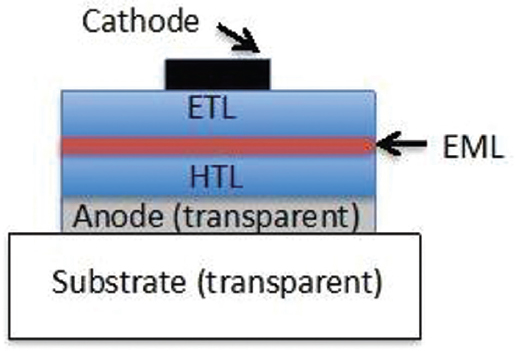
A simplified OLED structure is shown schematically in Figure 3.B.1. In this diagram, the nomenclature used is typical of that used in OLEDs. Here, “ETL” is the organic electron transport layer that moves electrons from the cathode metal contact to the light emissive layer, or “EML.” This layer is typically composed of two different molecules, a charge conductive “host” into which is doped at very small concentration (~1 to 8 percent by weight) of a molecule that gives off light of the desired color (or wavelength), under excitation from electrons and holes in the device. This dopant is called the light emissive “guest.” The “HTL” is the hole transport layer whose purpose is to transport positively charged “holes” from the anode contact to the EML. The transparent conducting anode through which the light is viewed is invariably composed of indium tin oxide (ITO), and the cathode is a metal (such as aluminum doped with lithium) capable of forming an ohmic contact with the ETL for the efficient injection of electrons. Typical OLED structures used in high-efficiency and high-reliability applications are considerably more complex than the structure shown in Figure 3.B.1. However, in all cases, the total thickness of organic layers rarely exceeds 100 nanometers (1 nanometer = 10−7 centimeter). The committee also notes that in contrast to LEDs, OLEDs can be made integral to the luminaire or fixture, rather than being added to it, in contrast to all alternative lighting solutions. This structural adaptability provides new design possibilities for solid-state lighting.
The mechanism for light emission in organic thin film OLEDs (see Box 3.B.1) is fundamentally different than in inorganic semiconductor LEDs described earlier in this chapter. When an electron, and its oppositely charged counterpart, the hole, are conducted to the same molecule within the EML, they put the molecule into an “excited state.” This excitation is maintained for a brief period of time (from nanoseconds to microseconds). While it exists, the excitation can hop from molecule to molecule which are very densely packed within the EML. This mobile excitation (called an “exciton”) eventually decays by the recombination of the electron and the hole: i.e., the electron “falls into” the hole which is located on the same molecule as the electron. This decay process often emits light whose energy is equal to that of the difference in energies between the electron and hole. By changing the composition or structure of the molecule,
the wavelength (color) of light emission can be varied. In fact, only slight chemical modifications can result in the color emission being changed from the ultraviolet, through the blue and green, to the red. In all cases, the light emission can be extremely efficient (100 percent conversion of electrons to photons has been reported across the visible light spectrum).
Metrics of Device Performance
In a manner similar to the calculation of external quantum efficiency (EQE) of an inorganic LED, the EQE of an OLED depends on both an intrinsic efficiency, for the material and device, and an outcoupling or extraction efficiency.
where ɸ is the absolute efficiency of a molecule to emit light once excited, γ is the probability that every injected electron and a hole can simultaneously exist on a light-emissive molecule, ηout is the outcoupling efficiency to be discussed below, and χ is the ratio of emissive molecular excited states that an electron and hole can reside on in a single molecule to the total number of possible excited states. χ is also known as the excited state ratio. For the best emissive molecules, ɸ = 1, which is often the case with state-of-the-art materials. Furthermore, γ = 1 in properly engineered device structures.
The power efficiency (ηP) of the light source is its most important operational parameter. Here the optical power out per the input electrical power is related to the quantum efficiency following:
Here, θ is the overlap of the light source with the spectral sensitivity of the eye, and Vλ is related to the energy of the emitted photon. The operating voltage of the OLED is V: clearly the power efficiency decreases as V increases. For a given device geometry, the operating voltage is related to the device drive current and thus also has an important influence on the device lifetime.
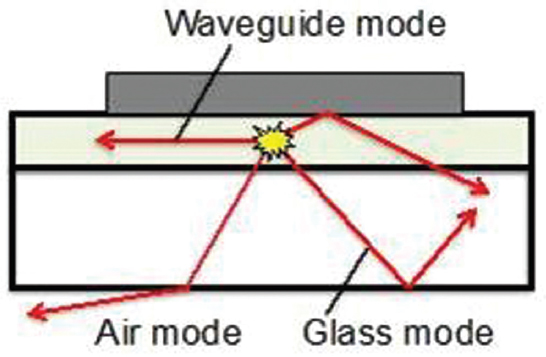
In conventional OLEDs fabricated on glass substrates, through mechanisms similar to those in inorganic LEDs, much of the emitted light is trapped within the glass substrate, or absorbed in the layers that comprise the device (see Figure 3.B.2), resulting in an extraction or outcoupling efficiency of only ~20 percent. However, low-cost schemes have been reported that can increase this efficiency to 40 to 60 percent (see below). Nevertheless, one of the grand challenges facing OLEDs is how to extract more of the emitted light in a cost-effective and highly efficient manner. This is discussed further in the section “Novel Approaches to Enhanced OLED Performance,” above.
Finally, the excited state ratio is χ = 0.25 for fluorescent emitting molecules, and χ = 1 for phosphors, as will be discussed in the following section (Baldo et al., 1999). Putting all of the efficiencies together, it is demonstrated that ηEQE = 20-60 percent in the very best cases. Even with these limitations, the power efficiency of phosphorescent white organic light emitting devices can exceed 150 lm/W, making them especially attractive for use as efficient lighting sources.
Architectures for White-Light OLEDs (WOLEDs)
White light in OLEDs is generated by mixing red, green and blue emission from different regions of the OLED. Several s¡chemes have been developed for OLED lighting applications that are both efficient and have a stable, predictable, and highly controllable white chromaticity. The highest performance is achieved using a variant of one of the three designs in Figure 3.B.3 depicts the striped white organic light emitting diode (WOLED), the fluorescent/phosphorescent (F/P) WOLED, and the stacked, or tandem WOLED. The latter design is most effective in achieving long lifetime and high brightness, and can be combined with the (F/P) design as well as others for illumination purposes.
Striped WOLEDs
This simple design places stripes of red (R), green (G), and blue (B) PHOLEDs (phosphorescent OLEDs) side-by-side. The R-G-B pattern is repeated on a very small scale so that the separate colors cannot be resolved by an observer. By injecting current into each stripe, the viewers will perceive the mixture of the three primary colors, which will appear white. An advantage of this design is that each of the three color elements can be separately optimized to emit with 100 percent internal efficiency, and variation of the current through each of the elements can be used to tune the color, from their constituent color to any desired white chromaticity. A disadvantage is the complexity of driving the WOLED with three different current sources.
F/P WOLEDs
This device is based on the recognition that approximately 25 percent of the color content of white light is blue. To achieve lower voltage operation and perhaps longer lifetime, this device uses a fluorescent blue segment, and harvests the remaining green and red excited states using phosphorescent molecular compounds. In principle, this particular device has the lowest drive voltage and hence highest efficacy of all alternative architectures. The F/P design can also be incorporated into stacked (tandem) and striped architectures. Hence, the device still achieves 100 percent internal quantum efficiency since all excitons are harvested by a combination of blue fluorescent dopants and red and green phosphors. Stacked WOLEDs (SOLEDs)
This compact design stacks two or three white emitting segments, with each segment separated by a very thin and transparent “charge generating layer.” In this case, a single
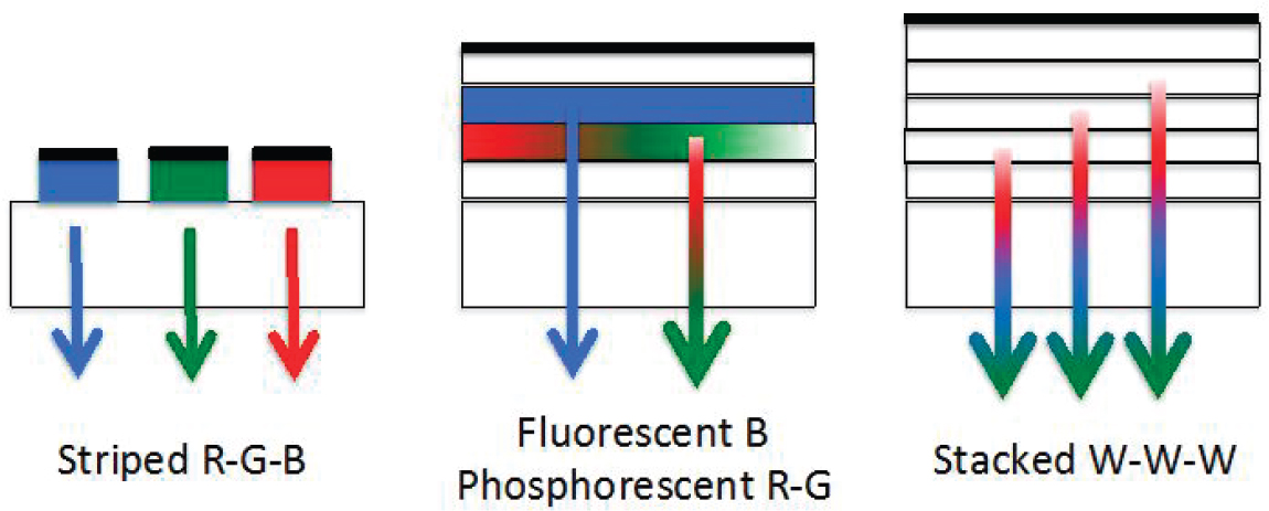
injected electron can recombine with a positively charged hole in each segment, generating a photon. Thus, a 2 to 3 times higher quantum efficiency is achieved with this device compared to the other designs, but at 2 to 3 times higher voltage (where the multiplier is equal to the number of elements in the final stack). Hence, the efficacy of this device is no higher than that of the other designs shown, but there are significant benefits of increased device lifetime.
References for Annex 3.B
Baldo, M.A., D.F. O’Brien, M.E. Thompson, and S.R. Forrest. 1999. The excitonic singlet-triplet ratio in a semiconducting organic thin film. Physics Review B 60:14422.
Helfrich, W., and W.G. Schneider. 1965. Recombination radiation in anthracene crystals. Physics Review Letters 14(1965):229.
Pope, M., H. Kallmann, and P. Magnante. 1963. Electroluminescence in organic crystals. Journal of Chemical Physics 38:2042.
Tang, C.W., and S.A. VanSlyke. 1987. Organic electroluminescent devices. Applied Physics Letters 51:913.


