
5
Manufacturing
INTRODUCTION
In the 3 years following the release of Assessment of Advanced Solid-State Lighting (NRC, 2013), the price of light-emitting diode (LED) lamps and luminaires has dramatically declined (see Figure 2.9). A dislocation of the LED market has been caused by significant oversupply created by the rise of a subsidized industry in China and the decline in the requirements for LEDs for the display market, due to the replacement of LED-lit liquid crystal displays (LCDs) by organic LED (OLED) displays in the hand-held market, and the need for a smaller number of higher-power LEDs in large LCD displays. LED-based lamps are now available for only a few dollars a lamp, with efficacies that are comparable or better than compact fluorescent lamps (CFLs). The cost and reliability of LED lamps and luminaires is signaling the end of incandescent bulbs, and replacement of fluorescent and other lighting, particularly in hospitality and retail. A restructuring of the solid-state lighting (SSL) industry has begun, precipitated by declining margins and a dissociation of the low-priced, high-volume commodity lighting business from the higher-profit-margin, lower-volume specialty lighting business. (See discussion in the section “Economic Drivers in the United States, Europe and Asia” below.) In addition, new applications of SSL (e.g., smart lighting and Li-Fi [Light Fidelity]) are providing new business opportunities for SSL manufacturers.
Key issues for SSL that relate to manufacturing include the supply chain, packaging (both at the package and luminaire level), system reliability, and lumen maintenance.
THE MANUFACTURING SUPPLY CHAIN AND ECONOMIC DRIVERS
LEDs
The supply chain is critical to the success of the manufacturing operation. Figure 5.1 shows a schematic of the manufacturing supply chain. The LED manufacturing process (shown in blue) is comprised of a sequence of relatively independent manufacturing steps (e.g., wafer fabrication, packaging, etc.) that are performed in the United States or offshore, mostly in Asia (see Table 5.1). The first step in the manufacturing process is epitaxial growth—the growth of the active device layer on a substrate. Epitaxial growth is performed using metal-organic chemical vapor deposition (MOCVD) reactors, as described in the section, “An LED Primer,” in Chapter 3. Because it is a highly proprietary technology, wafer fabrication, which includes epitaxial growth active films on a substrate wafer (usually sapphire), wafer dicing, and contact metallization, is usually done in-house by SSL manufacturers to safeguard their know-how. LED device fabrication, although primarily an in-house operation, particularly for the manufacture of high-power (HP) LEDs, is largely located in Asia for cost and supply chain reasons. For mid-power (MP) and low-power (LP) LEDs, there is a parallel supply chain with merchant LED die providing low-cost die to the major lighting product manufacturers and to packaging companies (e.g., Lextar, Taiwan). By far the largest suppliers of MP and LP LEDs are Epi Star in Taiwan and San’an in China.
The type of LED packages—containing separate LED die, phosphors, and encapsulation—depends on the power rating and optical characteristics of the LED. Details of several common LED packages are discussed in the section, “Packaging and Packageless LEDs.” Initial LED packaging is usually done in-house because of the proprietary nature of phosphor application, light extraction, and heat sinking technology inherent to the package design. Final packaging and testing of the completed LED are done in-house or outsourced to contract manufacturing suppliers. These various stages of packaging are almost exclusively done in facilities located in Asia.
The wafer fabrication and LED packaging processes are supported by a chain of suppliers, including manufacturing
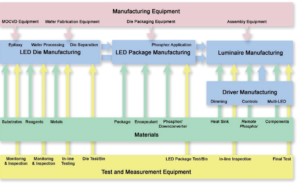
TABLE 5.1 Light-Emitting Diode (LED) Die, Packaging, and Luminaire Manufacturers
| Supply Chain | North America | Europe | Asia | |||
|---|---|---|---|---|---|---|
| Die manufacturing |
|
|
|
|
|
|
| LED package manufacturing | As above | As above | As above and:
|
|
||
| Luminaire manufacturing |
|
|
|
|
|
|
SOURCE: DOE (2016, p. 165).
equipment (shown in pink in Figure 5.1), testing (shown in yellow), and materials (shown in green).
There are several materials critical to LED manufacturing:
- Substrates. Substrates are the base material onto which the active layers are epitaxially grown. Substrates are 2 to 6 inches in diameter, with Sapphire growing to 8 inches and gallium nitride (GaN) available at 2 inches. In most cases, sapphire is the material of choice for the substrate, although some manufacturers use silicon carbide (SiC) and GaN.1 Sapphire wafers are available from global suppliers in all regions. SiC wafers are primarily sourced from the United States and used for LEDs by Cree, Inc.
- MOCVD precursors. The MOCVD precursors are the chemicals that are reacted in the gas phase to produce the epitaxial films that form the active layer structure of the LED. These precursors are organometallic compounds, which are available from suppliers located in all regions and are sourced globally (i.e., externally) by major manufacturers.
- Packaging materials. The specific materials used for the packages are dependent on the package design. For HP LED packages, aluminum nitride (AlN, a ceramic material) is generally used. These materials are primarily sourced in Asia. For MP and LP LEDs, plastic packages with copper lead frames (to carry electrical signals to/from the die) are used, which are also primarily sourced in Asia.
- Phosphor/down converters. The phosphor is a chemical compound that emits light of a certain frequency when excited by a light “pump.” There are a broad range of source materials available to make up the phosphors used for LEDs. Some phosphors are sourced internally (i.e., within the company) by major manufacturers, while others are provided by commercial suppliers located across the regions. The phosphor composition is often proprietary to the LED manufacturer.
- Encapsulation materials. The encapsulation materials are used to enhance light extraction and protect the device and the phosphors from the environment. Encapsulation materials are primarily silicones. In LP and MP devices, the phosphor is integrated with the silicone. These materials are sourced globally and provided by a number of suppliers located across all regions.
PACKAGING AND PACKAGELESS LEDS
LED packages provide mechanical support, heat removal, and electrical contact. The term LED means the active light-emitting device, which is the semiconductor device or the device covered with color conversion medium such as a phosphor. Packaging approaches have been developed for three broadly used categories of LEDs: (1) HP LEDs, which operate at power levels greater than 1 W; (2) MP LEDs, which operate at power levels between 0.25 W and 1 W; and (3) LP LEDs, which operate at less than 0.25 W. In addition, a new type of package technology called chip scale packaging (CSP; see the section, “Package-Free Technology,” below), also called package-free LEDs because they can be bonded directly to printed circuit boards, is gaining attention.
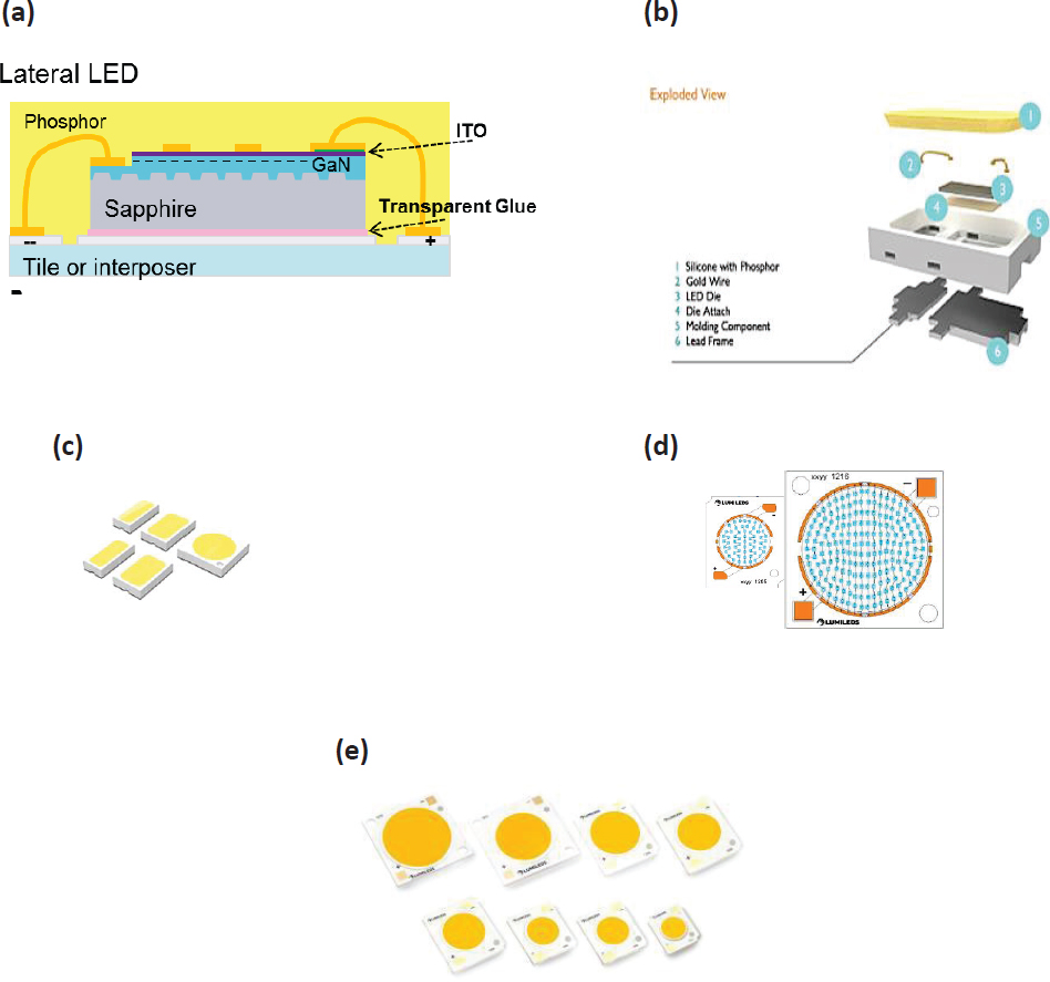
Low-Power and Medium-Power Packages
The largest quantities of LEDs used in illumination and LCD backlighting applications are of typically 0.5 W or lower power (i.e., MP or LP LEDs). These LEDs employ a device structure where light is emitted laterally through the edge of the die. With this structure, the light can more effectively couple into the phosphor converter. The schematic of the package is shown in Figure 5.2. The light emitted from the die travels into a plastic package “cup” with a silvered interior filled with phosphor material (shown in Figure 5.2b). The silvered cup also serves as a reflector to trap and couple the light to the phosphor. Due to its extremely low cost, this package is sometimes used for MP LEDs of powers higher than 0.5 W. Multiple lateral MP LED die can be arrayed together in a larger package, referred to as a “chip on board” (COB). These COBs have been rapidly gaining acceptance and created a lower cost solution compared to higher cost HP LEDs for directional lighting, such as polished aluminum reflector (PAR) lamps.
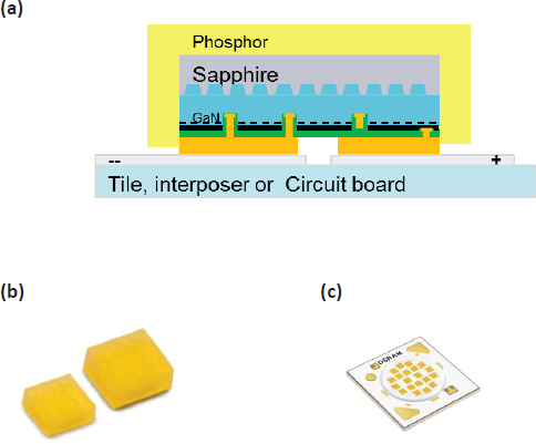
High-Power Packages
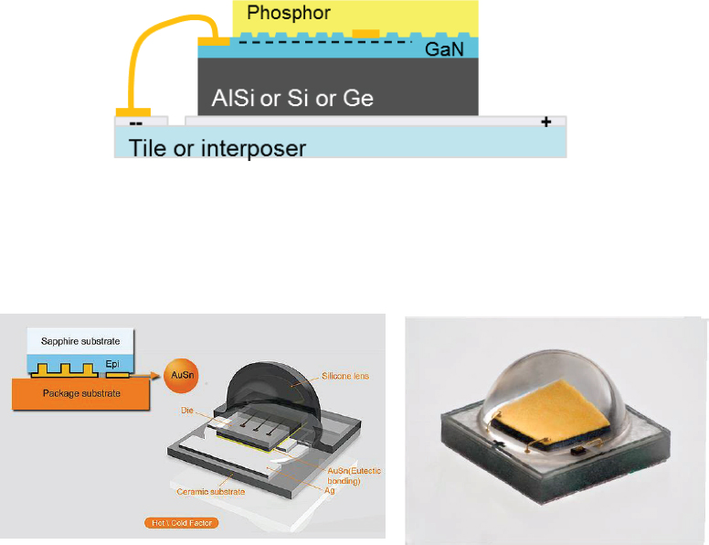
HP LEDs are packaged such that light is emitted from the top surface and are generally classed as “surface emitters.” In this design (shown in Figure 5.3), the sapphire substrate is removed from the epitaxially grown active layer, leaving a thin film of GaN containing the LED. The thin-film LED is then attached to a silicone, germanium, or ceramic carrier and covered in phosphor. The LED is then attached to a tile or interposer. This is the dominant packaging technology for HP LEDs, which can be implemented for flip-chip mounting, as shown in Figure 5.4. These architectures also often use a patterned sapphire substrate to improve light extraction.
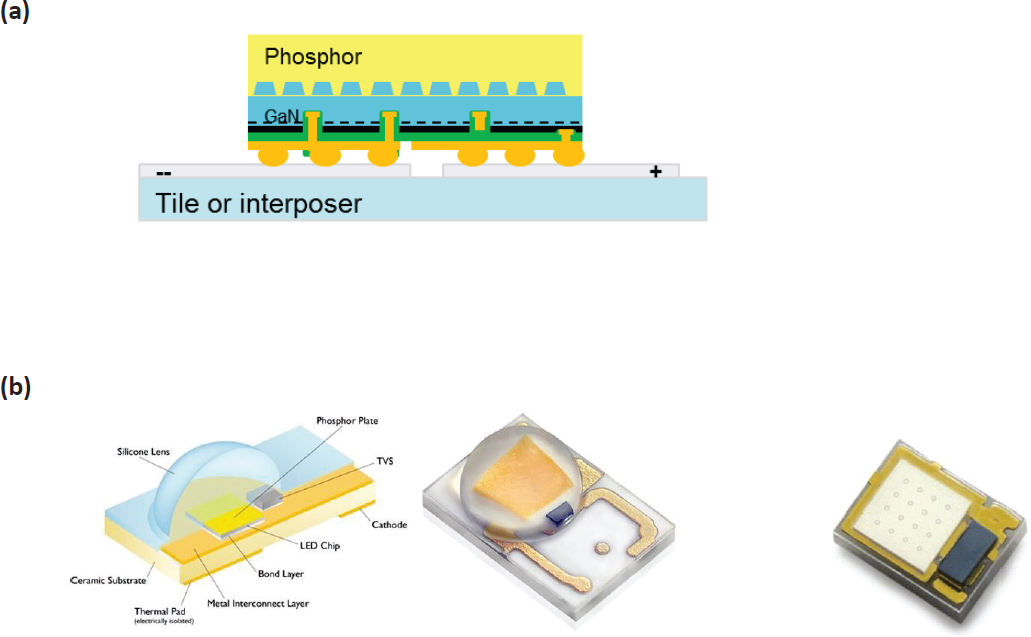
Package-Free Technology
The CSP is a stand-alone package die, which can be bonded directly to a printed circuit board. The CSP technology is illustrated in Figure 5.5. In this design the patterning of the sapphire substrate allows the sapphire to remain on the die as a structural support, while at the same time allowing light to be extracted through the top of the device. The
___________________
1 Including freestanding GaN substrates (for example, those offered by Soraa).
patterned sapphire substrate die has been critical in enabling CSP. These “package-free” die are low cost (compared with the thin film design in 5.3) and has a small size that can be packed at high density in a COB configuration as shown in 5.2d and operated at high power. This is the lowest cost packaging for HP LEDs.
A further advantage of this package is high device density, which results in a small light-emitting surface. The main disadvantage of the approach is that the light extraction efficiency is generally lower than the thin-film packages.
LAMPS AND LUMMINARES
The LED lighting industry is clearly separating the traditional lamp-based and luminaire-based business. Major players have taken steps to divest their lamp-based business, or at least separate their lamp-based business from their luminaire-based business. The lamp-based products are now seen as a commodity business with low profitability and insufficient product differentiation from various manufacturers. The luminaire-based business is increasingly being viewed as a better opportunity to drive increased values through technology integration (connectivity) and design innovation. Examples of this trend are GE, which separated its lamps business from its luminaire business by creating two new business units (Black, 2015), and OSRAM, which created a separate company into which it divested its general lighting lamps business (Prodhan, 2015).
Lamps/Lamp-Based Luminaires
LED lamps and LED lamp–based luminaires (luminaires with replaceable LED lamps) will continue to penetrate the general market because prices are currently low, even from top-tier manufacturers. It is expected that over time all conventional lamp types will be replaced by solid-state equivalents, including high-intensity discharge (HID) and linear fluorescent lamps. These conventional products offer little opportunity for differentiation.
In the LED lamp market, the focus is likely to be on further cost reduction. However, the investment in technology to drive the cost reduction is going to be limited, as the major players cannot realize appropriate returns. Instead, manufacturing of these commodity products has been moved to the lowest-cost locations. Already, LED lamp products are almost entirely manufactured in Asia. In spite of the limited investment in LED-based commodity lamps manufacturing, the price continues to decrease and the efficacy continues to rise, probably due to the fact that more-efficient LEDs are used along with smaller energy efficient electronics and smaller, more effective heat sinks.
FINDING: The domestic manufacturing of LED lamps and lamp-based luminaires is financially unattractive, as evidenced by U.S.-based manufacturers having either divested themselves of these product lines or segregated them operationally.
LED Luminaires (1st Generation)
Since the 2013 NRC report, the adoption of LED luminaires (luminaires with LED light engines2) has accelerated, particularly in areas such as outdoor, retail, hospitality, and industrial lighting. This financially attractive market is served by all SSL manufacturers, including many new entrants. It is being driven in part by specifications and regulations for energy efficient lighting in new installations and construction, as discussed in Chapter 2. This business space is becoming increasingly cost competitive and cannot indefinitely be viewed as a high-return business at the undifferentiated base-grade level.
Large-volume commercial and consumer luminaires are made in low-cost regions (see right-hand side of Figure 5.1). For specification- and architectural-grade luminaires, such as large, heavy outdoor fixtures, and low-volume professional configurable products, manufacturing is situated in regions close to the customer base, due to lead-time, shipping cost, and inventory management considerations. To this end, companies like GE and Philips are moving their manufacturing of these classes of products from the Far East back to North America.
LED Luminaires (Next Generation)
The next generation of LED luminaires will be defined by a combination of new design, performance, and control and connectivity features.
- Design (look and feel)—slim, transparent, unique form factor;
- Performance—light quality, control, efficacy; and
- Control and connectivity—integrating lighting functional control, other non-lighting features.
There is a strong belief that these products can reward innovation and offer differentiation. Often these luminaires will be low volume, highly customized, and project- or application-specific. The luminaire manufacturers can exploit the unique capabilities of LEDs to provide custom light appearance in retail applications as well as in adjacent markets of health care and horticulture. In addition, using luminaires based on edge-lit, light-guiding LEDs can create uniform light emitting surfaces similar to those created by OLED luminaires at a fraction of the cost. All these next-generation luminaires will be increasingly manufactured locally due to their complexity and customized features.
Luminaire product categories include the following:
- Base grade—products which meet limited specifications—often referred to as “consumer grade”;
___________________
2 LED light engines are LEDs with integrated drive electronics and/or optics.
TABLE 5.2 Ranking of LED Manufacturers by Revenue: The Largest 10 Players in the LED Industry Saw Their Revenues Shrink or Stay Level
| Rank | Company | Location | 2015 Revenues ($) | 2015 Share (%) | Growth in $USD (%) | Growth in Local Currency (%) |
|---|---|---|---|---|---|---|
| 1 | Nichia | Japan | 2,297 | 15 | −6 | 7 |
| 2 | OSRAM Opto | United States/Europe | 1,248 | 8 | −4 | 15 |
| 3 | Lumileds | United States/Europe | 1,196 | 8 | 4 | 4 |
| 4 | Samsung | South Korea | 960 | 6 | −18 | −18 |
| 5 | Seoul Semiconductor | South Korea | 801 | 5 | 0 | 7 |
| 6 | Cree | United States/Europe | 655 | 4 | −16 | −16 |
| 7 | LG Innotek | South Korea | 625 | 4 | −29 | −24 |
| 8 | Everlight | Taiwan | 590 | 4 | −6 | −6 |
| 9 | Mulinsen (MLS) | China | 561 | 4 | 2 | 2 |
SOURCE: Stephanie Pruitt, 2016, presentation at Strategies in Light, Santa Clara, Calif., March 1-3.
- Specification grade—products that meet specifications higher than base grade and are generally designed for professional installation; and
- Statement or architectural grade—the highest performance products from the perspectives of both performance and design.
ECONOMIC DRIVERS IN THE UNITED STATES, EUROPE, AND ASIA
Globally, government support for manufacturing varies widely from country to country. In the United States and Europe, the support has been focused on R&D and targeted manufacturing technology improvements, which represents encouraging but not significant sums. In stark contrast, from 2009/10 to the present, China has disrupted the global balance of the LED industry though massive subsidies to its domestic producers. In particular, China has provided huge subsidies for MOCVD reactors—the capital equipment for epitaxial growth, resulting in massive overcapacity of LED production and a rapid decline in LED price in recent years. The LED industry now sees marginal and even “irrational” pricing (product sold below cost), which is becoming an unsustainable norm, as the Chinese government continues to bolster its domestic LED industry through subsidies. Industry consolidation appears to be inevitable with an increasing number of LED companies merging or failing in the Chinese market.
China has also influenced the supply chain in the past by restricting the export of rare earth elements used in the phosphors. The response was an uproar worldwide, which also helped create new mining operations for rare elements in Australia and the United States.
Few companies in the LED lamp business are growing. It remains questionable whether the lamp and lamp-based luminaire market will offer a return on investment attractive to these companies in the short to medium term, or even in the long term, due to the reduced replacement market and the long life of LEDs. The data in Table 5.2 clearly illustrates this conclusion, showing that only two companies experienced growth in U.S. dollar–denominated revenue in 2015.
The conclusion that LED companies are not growing in the illumination business is reinforced by the actions of EPI Star in its recent downsizing of production capacity (Wang, 2016) and its announcement that for the first time it will increase LED die prices in June and then in July 2016. San’an, the largest Chinese supplier, is also taking steps to increase prices. Such moves are indicating that LED manufactures are unwilling to sell so far below cost just to maintain their market shares. Samsung, Philips, and others have taken actions in the past 2 years in restructuring their illumination-focused LED and lighting businesses.3 On the other hand, OSRAM (which separated from Siemens in 2013) has committed to investing heavily in the optoelectronics business with the belief that such investment in LED capacity and research will be justified in the long run (OSRAM, 2015).
To drive growth and profitability, LED companies are looking to high-value adjacent markets including infrared LEDs, ultraviolet LEDs, curing, connected lighting, horticulture, and medical applications. These adjacent markets are attractive as areas of potentially significant growth and profitability. Such technology-based markets in the past have been exploited with great success in the United States
___________________
3 The LED Lighting Exodus: Samsung Joins Philips and Siemens,” Memoori Smart Building Research, release date November 24, 2014.
through venture capital and entrepreneurial start-ups. SSLbased electronic products are an excellent fit to the venture model that relies on innovative product design and market acumen to drive new LED applications.
In addition to adjacent markets, the commercial and architectural luminaire business seems to be growing and remains financially attractive. Future markets, such as the Internet of Things, home and office controls, and ubiquitous information systems, are of great interest, and the luminaire may be an important hub for such systems. GE and other companies are enhancing their lighting businesses with development activities in these areas.
FINDING: Subsidies for China’s LED industry from the Chinese government have significantly impacted the global LED market, driving an oversupply of LEDs and resulting in price collapse and a rapid shift to a commoditized industry.
FINDING: The commoditization of the illumination market for LEDs has created an environment that is challenging for the LED industry and offers, in the short to medium terms, an unattractive return on investment for companies with business in LEDs.
OLEDS
The cost of OLED SSL products remains high at 20 to 25 times the $/lumen of comparable LED-based products. The capability of unique OLED products remains intriguing because, unlike LEDs that are a directional point source, the OLED is a diffuse-area light source distinguished by its spectral quality. Produced generally in the form of rigid or flexible tiles, OLED panels can be readily integrated to create luminaires without significant losses in efficacy or spectral quality. Because they are thin-film devices, OLEDs have the possibility of mass production by a high-speed, roll-to-roll process at a low cost. Compared to LED SSL products, OLED SSL products are in a very early stage of development, but they have made significant progress in that they are being produced by a number of manufacturers worldwide and sold in big-box stores. In terms of performance, commercial OLED SSL products have achieved an efficacy of 60 to 65 lm/W and a lifetime (L70) of 40,000 hours operating at a nominal surface luminance of 3,000 cd/m2.
OLED-SSL Products
Currently, the OLED-SSL business is very small compared to the LED SSL business. Worldwide, there are fewer than a dozen OLED panel manufacturers and even fewer OLED luminaire makers. LG Display of Korea, with business mainly in LCD and OLED displays, is the leading OLED-SSL manufacturer, after it acquired the OLED-SSL business from LG Chem in 2015. OLEDWorks is the sole OLED-SSL manufacturer in the United States. Begun as an R&D enterprise in Rochester, New York, it became a global OLED-SSL manufacturer after acquiring the OLED-SSL business and manufacturing facilities from Philips of Germany in 2015. Konica-Minolta, First-O-Lite, and OSRAM are other key players in Japan, China, and Germany, respectively. In Table 5.3, representative OLED-SSL products from these and other manufacturers are listed along with their product specifications.
It can be seen that there are significant variations in the key performance metrics—efficacy and lifetime—among OLED-SSL products from various manufacturers, reflecting that OLED products are far from standardized, and their commercialization is still at an early stage. The highest efficacy is 60 to 65 lm/W (by LGD and First-O-Lite), and the longest lifetime (L70) is 40,000 to 50,000 hours (by LGD and Kaneka) for nominal operation of about 3,000 cd/m2 in surface luminance. The color rendering index for OLED-SSL is generally high, ranging from 80 to more than 90 for all products. The drive voltage varies over a large range (from 6 V to over 20 V) due to the adoption of various tandem structures in OLED-SSL products. LGD products have a 2- or 3-stack tandem structure, which requires a drive voltage of 6.1 V and 8.5 V, respectively, whereas OLEDWorks products incorporate a six-stack tandem structure, resulting in a much higher drive voltage of 20 V (and also a proportionally higher luminance). While the adoption of tandem structures is essential to achieving high brightness and long lifetime in OLED-SSL products, it also incurs extra cost in manufacturing due to the increased complexity of the tandem structures and the requirement of extra deposition chambers.
OLED-SSL Product Cost
The high cost of OLED-SSL products has been the key barrier to their adoption for general lighting applications. While the cost of conventional LED-SSL products has dropped precipitously and their mass adoption is being rapidly realized, the cost of OLED-SSL products has remained extraordinarily high by comparison, and their utility so far is limited to specialty lighting. In benchmarking the lumen cost of LED and OLED products, the customary metric dollar per kilo-lumen ($/klm) is used. Table 5.4 lists the high, low, and average lumen cost values for 10 LED-SSL edge-lit panel products available today from Amazon.com. For comparison, the costs of four OLED-SSL products (two from Acuity Brands sold at Home Depot and two from the OLEDWorks catalog) are also listed.
The high cost of OLED-SSL is largely due to the high cost of manufacturing OLED panels. A recent study by Bardsley has provided an estimate of the breakdowns of the
TABLE 5.3 Comparison of LED and OLED Product Specifications
| Company: | LGD | LGD | OLEDWorks | OSRAM | Kaneka | Lumiotec | Mitsubishi Chemical First-O-Lite | |
|---|---|---|---|---|---|---|---|---|
| Product Model: | N6SD30C | P6BD30A | FL300 | SDW058 | KNPP4BF3 0 | P04B0405L A13A | Velve 52800 | FOLB002 |
| Substrate type | Glass | Plastic | Glass | Glass | Glass | Glass | Glass | Glass |
| Shape | Square | Rectangle | Square | Square | Square | Square | Square | Rectangle |
| Lit size (mm × mm) | 300 × 300 | 41 × 394.2 | 102 × 102 | 105 × 105 | 80 × 80 | 125 × 125 | 123 × 123 | 102.4 × 47.5 |
| Lit area (m2) | 0.0900 | 0.0162 | 0.0104 | 0.011 | 0.0064 | 0.0156 | 0.0151 | 0.0048 |
| Flux (lumen) | 800 | 150 | 300 | 68 | 60 | 145 | 48 | 45 |
| Efficacy (as quoted) (Lm/W) | 600 | 50 | 40-50 | 40 | 42 | none | 31 | 65 |
| CCT (Deg K) | 3,000 | 3,000 | 3,000 | 3,400 | 3,000 | 2,800 | 2,700-6,500 | 3,000 |
| CRI | 90 | 85 | 80 | 80 | 86 | 80 | >80 | >90 |
| LT70 (as quoted) (Hr) | 40,000 | 20,000 | 10,000 | 10,000 | 50,000 | 10,000 | 20,000 | 20,000 |
| DC volt (V) | 8.5 | 6.1 | 20 | 6 | 6.8 | 8 | 24 | 8.6 |
| DC current (mA) | 1600 | 490 | 358 | 285 | 210 | 450 | 110 | 80.8 |
| Power (W) | 13.60 | 2.99 | 7.16 | 7.71 | 1.43 | 3.60 | 2.64 | 0.69 |
| Current density (Cal) (mA/cm2) | 1.78 | 3.03 | 3.44 | 2.59 | 3.28 | 2.88 | 0.73 | 1.67 |
| Luminance (cd/m2) | 2829 | 2954 | 9178 | 1975 | 2984 | 2954 | 1010 | 2960 |
NOTE: LGD = LG Display.
TABLE 5.4 Comparison of the Lumen Cost Between Light-Emitting Diode (LED) and Organic Light-Emitting Diode (OLED) Solid-State Lighting (SSL) Products
| High-Low and Average of $/klm | High | Low | Average |
|---|---|---|---|
| LED SSL (luminaires) a | 50.6 | 17.5 | 33.5 |
| OLED-SSL (mix of luminaires and lamps) | 1463 | 237 | 735.1 |
a Edge-lit panel.
various costs associated with the manufacture of OLED-SSL products.4
Table 5.5 shows the projected cost reductions from 2014 to 2025, assuming essentially the economy of scale in terms of large increases in production capability and lowering the bill of materials. These assumptions include the scaling of the factory size from the current Generation 2 (G2) factory for substrate area of 0.17 m2 to the G8 factory for substrate area of 5.5 m2. The overall cost reduction goal is almost 20 fold from $1,850/m2 in 2015 to $100/m2 in 2015. In terms of lumen cost (assuming a Lambertian emitter of 3,000 cd/m2), the equivalent reduction is from 196 $/klm to 10.6 $/klm. It is interesting to note that the estimated value of 196 $/klm for 2015 from Bardsley is in approximate agreement with the low-end cost value of 237 $/klm for OLED-SSL products in Table 5.5.
TABLE 5.5 The Department of Energy’s Cost Reduction Goals
| 2014 | 2015 | 2017 | 2020 | 2025 | |
|---|---|---|---|---|---|
| Substrate area | 0.17 | 0.17 | 1.38 | 2.7 | 5.5 |
| Capital cost ($ million) | 75 | 75 | 200 | 300 | 400 |
| Cycle time (minutes) | 3 | 2 | 2 | 1 | 1 |
| Capacity (1,000 m2/year) | 14 | 25 | 300 | 1,000 | 2,400 |
| Depreciation ($/m2) | 1,050 | 600 | 125 | 60 | 35 |
| Organic materials | 200 | 150 | 100 | 35 | 15 |
| Inorganic materials | 200 | 200 | 120 | 50 | 30 |
| Labor | 150 | 100 | 20 | 10 | 5 |
| Other fixed costs | 75 | 50 | 15 | 10 | 5 |
| Total (unyielded) ($/m2) | 1,675 | 1,100 | 355 | 160 | 90 |
| Yield of good product (%) | 50 | 60 | 70 | 80 | 90 |
| Total cost ($/m2) | 3,350 | 1,850 | 550 | 200 | 100 |
SOURCE: J.N. Bardsley, 2016, “OLED Manufacturing Challenges,” presented at DOE Solid-State Lighting R&D Workshop. Raleigh, N.C., February 3.
It is expected that the cost of OLED-SSL products will continue to fall in future years as a result of the explosive growth in the OLED display industry. The most recent (4Q 2015) cost estimate for a 5” full-high-definition active-matrix OLED (FHD AMOLED) display (for smartphones) by IHS is $14.30, which is—for the first time—lower than the cost of an equivalent LCD display. Using this cost figure and assuming conservatively that one-third of the AMOLED panel cost is due to the OLED component (i.e., excluding thin film transitor backplane, drivers, red, green, blue pix-elation), the cost of the OLED component is $697/m2 or 74 $/klm in terms of lumen cost. Based on this cost assessment and assuming that OLED-SSL is equivalent to or no more expensive than the OLED component of the AMOLED display, Bardsley’s 2015 cost target of $1,850/m2 or 196 $/klm for OLED-SSL products has been more than substantiated. However, the cost of OLED-SSL products remains too high to be competitive with today’s LED-SSL products. Further steep cost reductions, as targeted in Bardsley’s report, will be needed for OLED-SSL products to emerge as a viable business in general or specialty lighting sectors.5
FINDING: Very aggressive manufacturing cost reductions will be necessary for OLED-SSL to be a successful entrant to the general lighting markets in the near future.
OLED-SSL Manufacturing
The manufacturing supply chain for OLEDs mainly includes equipment for thin-film deposition and encapsulation and chemical materials for the OLED layers. Asian companies are clearly dominant in the area of equipment, although there are some recent notable entries from the
___________________
4 J. Norman Bardsley, 2016, “OLED Manufacturing Challenges,” presented at DOE Solid-State Lighting R&D Workshop, Raleigh, N.C., on February 3.
5 Ibid.
TABLE 5.6 Major Companies in OLED Manufacturing
| Category | Companies |
|---|---|
| Deposition/Encapsulation | Cannon Tokki, Ulvac, Seiko Epson, AP Systems, Sunic, SNU, SFA Engineering, AMAT, Kateeva, Axitron |
| Materials | Samsung SDI, LG Chemical, Dooson, SFC, Duksan, Idemitsu Kosan, Hodogaya, Toyo Ink, UDC, Dow Chemicals, Merck |
United States, whereas the chemical business is more globally distributed.
Table 5.6 lists the major companies in these two sectors. Almost all of these companies target OLED display industry as the key business, as the OLED lighting industry is so far miniscule in comparison. The equipment business is dominated by only a few companies, notably Canon Tokki of Japan and Sunic of Korea—both supply production-scale OLED thin-film deposition equipment of G6 and above. U.S. equipment makers include large companies such as AMAT, which provides large-area physical-vapor-deposition equipment for both OLED and the TFT backplanes, and small start-ups such as Kateeva, which provides large-area inkjet deposition equipment for RGB patterning and encapsulation. The material business is considerably more fractured compared to the equipment business, largely due to the need for a large number of different emitting and charge-transport materials comprising the multi-layers in the OLED stack. Material suppliers tend to limit their business to specific categories of materials. Idemitsu Kosan of Japan, for instance, is known as the major supplier for blue fluorescent materials, including both host and dopant molecules. To a large extent, their business is supported by their strong intellectual property (IP) position in the blue fluorescent emitter technology. Likewise, Universal Display Corp. (UDC), a U.S.-based company, has dominated the business of phosphorescent OLED materials due to their strongly held IP position in iridium-based emitters.
Current OLED-SSL products are manufactured using G2 vapor-deposition tools (capable of handling mother-glass size of 370 mm × 470 mm). Planned installation of G5 tools for OLED-SSL products (1,100 mm × 1,200 mm) was recently announced by LGD. Estimated capital cost, including clean rooms and support facilities, is $75 million for a G2 tool, $200 million for G5, and $400 million for G8 (2,200 mm × 2,500 mm).6 To reduce capital cost, high-speed, roll-to-roll solutions or vapor-deposition processes are being developed for the manufacture of flexible OLED-SSL products. Konica Minolta and Sumitomo Chemical of Japan are leading such efforts with focus on solution-processed, polymer-based OLEDs by the latter. Unlike OLED display products, OLED-SSL products are more suited for roll-to-toll manufacturing as they do not require high-density pixilation. Although it promises to significantly reduce cost, the roll-to-roll process has yet to be adopted as a production tool for flexible OLED-SSL products. Today’s flexible commercial OLED products, including displays and SSL, are manufactured using a standard vapor-deposition process involving rigid plates.
Huge investments are being made in the OLED display industry to lower the cost of producing OLED displays, including developments in alternative substrates, lower-cost materials, large-area inline tools, reduced tact time, and robust thin-film encapsulation, all of which are transferrable to the development of OLED-SSL products. Rapid cost reduction in OLED-SSL manufacturing is to be expected with the maturity of the OLED display industry.
Both OLED-SSL and OLED-TV products are based on white tandem OLED technology and share similar manufacturing processes. OLED-SSL will directly benefit from the advances made in OLED-TV in terms of technology development and cost reduction.
Light extraction is an essential component in OLED-SSL that is not shared by OLEDs for displays. Internal light extraction is deemed to be important, but robust and low-cost methods for its implantation in OLED-SSL has not yet been developed.
FINDING: OLED-SSL manufacturing cost is high due to high cost of capital equipment and materials. The rapid growth of the OLED display industry should have a positive impact on the cost reduction of OLED-SSL products in the near future.
REFERENCES
Black, T. 2015. GE splits lighting to form LED unit as $5 billion in sales seen. Bloomberg. October 7. https://www.bloomberg.com/news/articles/2015-10-07/ge-splits-lighting-to-form-led-unit-as-5-billion-insales-seen.
DOE (U.S. Department of Energy). 2015. Solid-State Lighting R&D Plan. Washington, D.C. May.
DOE. 2016. Solid-State Lighting R&D Plan. Washington D.C. June.
OSRAM. 2015. “Investments of About €3 Billion Create New Growth Prospects for Osram.” Press release. November 11. https://www.osram.com/osram_com/press/press-releases/_business_financial_press/2015/investments-of-about-3-billion-create-new-growth-prospects-for-osram/index.jsp.
Prodhan, G. 2015. Osram to separate from lamps and focus on automotive. Reuters. April 21. http://www.reuters.com/article/us-osram-lichtdivestiture-idUSKBN0NC1NG20150421.
Wang, L. 2016. Epistar announces plan to shut down Taoyuan production. Taipei Times. May 24. http://www.taipeitimes.com/News/biz/archives/2016/05/24/2003646961.
__________________
6 Ibid.


