
5
Quantum Sensors
Susan Sinnott, Pennsylvania State University, introduced three speakers who discussed quantum sensors: Philip Hemmer, Texas A&M University; Mohammad Soltani, Raytheon BNN Technologies; and David Awschalom, University of Chicago. Robert Hull, Rensselaer Polytechnic Institute, moderated short Q&A periods that followed each talk.
QUANTUM SENSORS, IMAGING, AND LITHOGRAPHY
Philip Hemmer, Texas A&M University
Hemmer’s work, involving the fabrication of fluorescent color centers in diamonds to advance molecular imaging, highlights key challenges and opportunities in quantum sensing, imaging, and lithography applications.
Materials Drive Progress
Having the right materials strongly influences progress toward quantum technology applications. Researchers often have great ideas but then face the barrier of finding (or creating) the materials required to implement them.
When Hemmer began studying quantum information, he sought a solid-state material that could operate like trapped ions, but with increased functionality, like electrically tuning qubits into resonance with each other using electrodes. This led to a focus on nitrogen-vacancy (NV) centers. As the quality of available materials
increased, Hemmer and collaborators were able to make the first working photonic structures in diamond1 and eventually to demonstrate spin-photon entanglement with NV.2
Building on the team’s rapid progress with improved materials, other researchers had good results at room temperature, for example, in the development of a quantum memory with long storage time.3 Hemmer and collaborators were able to achieve entanglement with NV with a long survival time,4 and NV-N pairs close enough together could create a scalable entanglement,5 suggesting the potential of a room-temperature quantum computer. Hemmer and collaborators also demonstrated a single-shot readout,6 underscoring diamond’s tremendous potential as a quantum material.
Materials Challenges and Solutions
Unfortunately, in the midst of this exciting research, funding disappeared, materials improvement plateaued, and much of the materials work went overseas. There, researchers were able to accomplish teleportation with NV,7 while in the United States NV research progressed slowly. In particular, efforts to suppress unwanted interactions between NVs and surface spins were based largely on trial- and-error approaches.
The long-awaited solution to increased progress for spin-photon entanglement was hidden in plain sight: silicon vacancy (SiV). SiV was thought to have terrible
___________________
1 T.M. Babinec, B.J.M. Hausmann, M. Khan, Y. Zhang, J.R. Maze, P.R. Hemmer, and M. Lončar, 2010, A diamond nanowire single-photon source, Nature Nanotechnology 5:195-199, https://doi.org/10.1038/NNANO.2010.6.
2 E. Togan, Y. Chu, A.S. Trifonov, L. Jiang, J. Maze, L. Childress, M.V.G. Dutt, A.S. Sørensen, P.R. Hemmer, A.S. Zibrov, and M.D. Lukin, 2010, Quantum entanglement between an optical photon and a solid-state spin qubit, Nature 466:730-734, https://doi.org/10.1038/nature09256.
3 P.C. Maurer, G. Kucsko, C. Latta, L. Jiang, N.Y. Yao, S.D. Bennett, F. Pastawski, et al., 2012, Room-temperature quantum bit memory exceeding one second, Science 336(6086):1283-1286, https://doi.org/10.1126/science.1220513.
4 P. Neumann, N. Mizuochi, F. Rempp, P. Hemmer, H. Watanabe, S. Yamasaki, V. Jacques, T. Gaebel, F. Jelezko, and J. Wrachtrup, 2008, Multipartite entanglement among single spins in diamond, Science 320(5881):1326-1329, https://doi.org/10.1126/science.1157233.
5 T. Gaebel, M. Domhan, I. Popa, C. Wittmann, P. Neumann, F. Jelezko, J.R. Rabeau, et al., 2006, Room-temperature coherent coupling of single spins in diamond, Nature Physics 2:408-413, https://doi.org/10.1038/nphys318.
6 P. Neumann, J. Beck, M. Steiner, F. Rempp, H. Fedder, P.R. Hemmer, J. Wrachtrup, F. Jelezko, 2010, Single-shot readout of a single nuclear spin, Science 329(5991):542-544, https://doi.org/10.1126/science.1189075.
7 W. Pfaff, B.J. Hensen, H. Bernien, S.B. van Dam, M.S. Blok, T.H. Taminiau, M.J. Tiggelman, R.N. Schouten, R.N. Schouten, M. Markham, D.J. Twitchen, and R. Hanson, 2014, Unconditional quantum teleportation between distant solid-state quantum bits, Science 345(6196):532-535, https://doi.org/10.1126/science.1253512.
optic properties, but researchers learned that these properties actually depended strongly on the diamond being used. With a good diamond, SiV actually had very good optic properties, plus its inversion symmetry suppressed much of the spectral diffusion that limited the NV. With this color center, experiments that had failed, or were very difficult before, were now successful.
In response to a workshop participant’s question, Hemmer noted that working with SiV still presents difficulties, which is why germanium vacancy (GeV) is now being explored. GeV is much brighter and has better performance, but there are problems with its light emission that are believed due to a trade-off between crystal growth speed needed to create GeVs and the resulting crystal purity.8
Quantum Techniques for Molecular Imaging
A driving goal of Hemmer’s research is to use quantum properties to image proteins in live cells. Toward this end, Hemmer and collaborators devised a way to improve magnetic resonance imaging (MRI) using an NV to detect changes in the magnetic field produced by nearby electron or nuclear spins in the presence of a nanoscale magnetic gradient.9,10 One problem with this method, however, was that it was done on a bulk crystal, but defects in nanodiamonds that trap electron spins prevent the observation of nuclear spins in live cells.
The ideal diamonds for this application would have to be incredibly small, the team realized, and include a color center. Growth conditions are also crucial: fast diamond growth can trap impurities and cause strain. After unsuccessfully testing several known methods for making nanodiamonds, the team developed a revolutionary method that produced very pure diamonds with no strain: engineering fluorescent nanodiamonds through a bottom-up fabrication process using high pressure. The method, which Hemmer described as a cross between crystal growth and chemical synthesis, uses diamond-like molecules as seeds.
The envisioned next step for this work is to grow a scalable quantum computer with storage registers at room temperature, using these grown nanodiamond color centers. Putting this computer into a live cell will give the nanoscale MRI readout, and a similar method could also work for building an optical quantum computer, something else Hemmer is exploring.
___________________
8 P. Siyushev, M.H. Metsch, A. Ijaz, J.M. Binder, M.K. Bhaskar, D.D. Sukachev, A. Sipahigil, et al., 2017, Optical and microwave control of germanium-vacancy center spins in diamond, Physical Review B 96081201(R), https://link.aps.org/doi/10.1103/PhysRevB.96.081201.
9 B. Grotz, J. Beck, P. Neumann, B. Naydenov, R. Reuter, F. Reinhard, F. Jelezko, J. Wrachtrup, D. Schweinfurth, B. Sarkar, and P. Hemmer, 2011, Sensing external spins with nitrogen-vacancy diamond, New Journal of Physics 13:055004, https://doi.org/10.1088/1367-2630/13/5/055004.
10 P. Hemmer, 2013, Toward molecular-scale MRI, Science 339(6119):529-530, https://doi.org/10.1126/science.1233222.
Looking Ahead
As they continue to work with diamonds, rare-earth elements, and techniques to determine color centers and their implications, Hemmer and his team are focused on identifying the best materials for quantum applications, developing techniques for mass production, and identifying new color centers with enhanced single-shot room-temperature readout, which will enable many other quantum technologies.
For continued progress toward quantum tools, both the right materials and the right domestic manufacturing infrastructure will be critical. Hemmer’s need for appropriate materials led to his discovery of a new way to grow diamonds with the right properties, and his goal of biomolecule imaging in a live cell is now much closer.
Asked why the coherence length in isotopically pure diamond was longer, Hemmer clarified that it had to do with the magnetic noise produced by the carbon 13 atoms, and the biggest improvement was in the inhomogeneous width that is observed for longer time scales. He noted that his team is also trying similar experiments with isotopically enriched seed and growth material.
Asked to speculate on the reasons for the lack of funding in this area, Hemmer noted that this work is so high risk that funders are reluctant to support it. In addition, for many years diamonds were not seen as potential quantum materials. Asked what could reinvigorate domestic materials work, Hemmer noted that the U.S. Navy, U.S. Air Force, and U.S. Army research laboratories are already supporting pilot efforts, and other researchers need to be connected to funding sources. The Chinese satellite launch has inspired a competitive international arena, he added, suggesting that U.S. agencies may be more willing to fund this kind of research going forward.
QUANTUM TRANSDUCERS ON INTEGRATED PHOTONIC PLATFORMS
Mohammad Soltani, Raytheon BBN Technologies
Soltani highlighted quantum research being pursued at Raytheon BBN Technologies in photonics, superconducting qubits, and particularly in the area of quantum transducers and integrated photonic platforms, and described future research directions. Raytheon BBN researchers are involved in developing a range of core capabilities for quantum, including photonics, superconducting quantum technologies, and in-house fabrication capabilities. The team hosts academic collaborations and also works on algorithms, programming languages, classical
controls, and various devices, with a particular focus on superconducting and optical technology.
Transduction
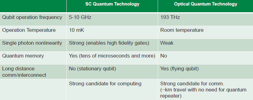
Superconducting and optical quantum technologies have very different characteristics, including different qubit operation frequency, operation temperature, single-photon nonlinearity strength, and memory and long-distance capabilities (Figure 5.1). Because of these differences, superconducting and optical quantum technologies lend themselves to different applications. There is therefore a need for mechanisms to interface between quantum platforms to connect various applications such as computing and communication.
Superconducting quantum technologies offer particular promise for quantum computing, although they typically require cryogenic temperatures. Optical quantum technology has strong potential for quantum communication and information transfer, and can work at room temperature. To move the technology forward and lay the groundwork for interfaces between quantum computers and quantum communications networks, Soltani said the next step is to translate what is possible cryogenically to room temperature, while maintaining quantum coherence. This requires a transduction mechanism to convert a quantum signal from a cryogenic platform to a room-temperature platform.
Such a transducer, Soltani noted, would have many applications, even beyond quantum, such as for clock synchronization and next-generation probes in the microelectronics industry. Researchers have experimented with different schemes for transduction, including optomechanics, piezo-mechanics, magnon, and electrooptics. Each method has benefits and drawbacks.
Electro-Optics
Electro-optics are more scalable than other approaches, although it will still take many years to get to the required transduction efficiency, Soltani said. In this scheme, an electro-optic mixer combines a microwave signal (from superconducting qubits) with an optical signal, thereby converting the microwave frequency as an upper frequency sideband to the optical frequency. While that is a good outcome, unfortunately it also creates a noisy down-conversion sideband on the lower side of the optical frequency. Furthermore, the pump power required is more than a dilution refrigerator can handle, causing it to overheat and break the superconducting regime. Despite these drawbacks, this research is still advancing the overall field, and whispering-gallery-mode electro-optic resonators have enabled the team to achieve efficient coupling of light from silicon waveguides to resonators.11
On an additional path, Soltani’s group, in collaboration with Harvard University, showed that it was possible to generate more efficient and low-noise electro-optic quantum transduction using compact integrated electro-optic coupled resonators.12 Harvard researchers have experimentally demonstrated integrated nanophotonic electro-optic resonators on a chip with quality factors of 10 million, a significant improvement resulting in much higher g factors.13 Those results made it possible to couple a nanophotonic resonator with doublet resonance integrated with a microwave resonator, providing an ultracompact, triply resonant system with enhanced g and suppressed lower sideband, which is the noise. Soltani’s group is continuing to build on this progress by expanding into other materials, which could bring more advances.
Future Directions
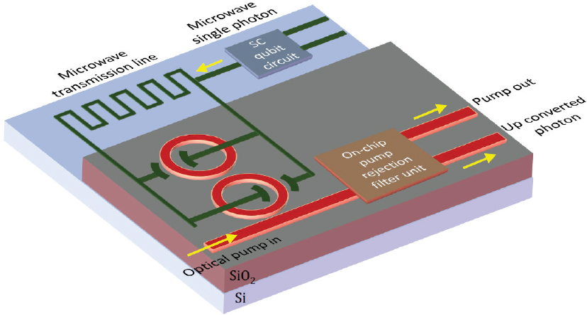
Together, Soltani’s team and the Harvard team are working toward a vision for monolithic quantum transduction on a chip, see Figure 5.2. Significant enhancements in conversion factor (also known as g factor) have been demonstrated, although there is still noise. To reduce noise, it will be necessary to reduce optical
___________________
11 M. Soltani, V. Ilchenko, A. Matsko, A. Savchenkov, J. Schlafer, C. Ryan, and L. Maleki, 2016, Ultrahigh Q whispering gallery mode electro-optic modulator resonators on a single photonic chip, Optics Letters 41(18):4375-4378, https://doi.org/10.1364/OL.41.004375.
12 M. Soltani, M. Zhang, C. Ryan, G.J. Ribeill, C. Wang, and M. Lončar, 2017, Efficient quantum microwave-to-optical conversion using electro-optic nanophotonic coupled resources, Physical Review A 96:043808, https://link.aps.org/doi/10.1103/PhysRevA.96.043808.
13 M. Zhang, C. Wang, R. Cheng, A. Shams-Ansari, and M. Lončar, 2017, Monolithic ultrahigh-Q lithium niobate microring resonator, Optica 4(12):1536-1537, https://doi.org/10.1364/OPTICA.4.001536.
pump power, which Soltani suggested could happen within the next 5-10 years, although having the right materials will be essential.
Broadly speaking, key capabilities of interest moving forward include achieving large g factors; high transducer efficiency, scalability, and high thermal/mechanical stability; and tunability; the desired range for required optical resonator Q, required microwave resonator Q, and optical pump power; and high fidelity of transferred Fock state, all without any suspended components.
Soltani said developing integrated photonics at cryogenics is a key enabler to all of these features, and indeed to many other quantum technologies. However, there are still remaining challenges to achieve ultra-low-loss devices, efficient coupling, efficient photonic functionalities at low temperatures, and efficient photonic filters. Materials, especially those that can work with microwaves and optical domains at the same time, with low loss in both domains, are essential, Soltani concluded.
Asked if his group had considered sodium and potassium niobates, Soltani said that they were open to any materials that held the most potential, can be made as a thin film, are compatible with planar microfabrication, and show the scalability path. Another participant asked whether Raytheon has a time frame to meet the milestones Soltani described. Soltani answered that low-efficiency transducers are expected in the 3- to 5-year time frame, but achieving 80 percent efficiency will take longer because there are still so many technology gaps.
DRIVING QUANTUM SCIENCE AND ENGINEERING WITH SEMICONDUCTORS
David Awschalom, University of Chicago
Awschalom discussed progress and challenges related to materials and manufacturing, needed quantum components, and the detecting and sensing instrumentation necessary to move research advancements from science to technology.
Materials and Manufacturing
Recent years have brought important progress in quantum research and technology. The energy scale for quantum state control has risen, allowing for exclusive control over individual electrons and nuclei, long particle spin coherence at room temperature, and the tantalizing possibility of scalable systems, Awschalom said. Much of this work is being carried out in other countries. Researchers in Australia demonstrated a single-electron spin-based qubit; and in Japan, scientists showed the ability to control a single nuclear spin, and these results revealed impressively long quantum coherence times.14,15
Materials, often made in Japan, were integral to these advancements. Awschalom noted that limitations in the current U.S. materials infrastructure are to some extent constraining progress. Nonetheless, U.S. researchers are making strides, frequently working with materials produced abroad. Awschalom highlighted the Petta Physics Laboratory at Princeton University and the Eriksson Physics Laboratory at the University of Wisconsin, which have both used silicon, germanium, and other well-known standard device materials to demonstrate high-fidelity single qubit gates, tunable electron states, and prototype quantum gates. Perhaps most importantly, he said that work presents a path toward a scalable quantum information technology platform.
New materials frameworks, such as silicon carbide, can have a very large impact, Awschalom said. Density functional theory research accurately predicted that silicon carbide, already prevalent in lighting, micromechanical sensing, and high-powered electronics, is a viable candidate for quantum information processing, as it demonstrates very good coherence at room temperature with the
___________________
14 J.J. Pla, K.Y. Tan, J.P. Dehollain, W.H. Lim, J.J.L. Morton, D.N. Jamieson, A.S. Dzurak, and A. Morello, 2012, A single-atom electron spin qubit in silicon, Nature 489(7417):541-545, https://doi.org/10.1038/nature11449.
15 J.T. Muhonen, J.P. Dehollain, A. Laucht, F.E. Hudson, R. Kalra, T. Sekiguchi, K.M. Itoh, D.N. Jamieson, J.C. McCallum, A.S. Dzurak, and A. Morello, 2014, Storing quantum information for 30 seconds in a nanoelectronic device, Nature Nanotechnology 9:986-991, https://doi.org/10.1038/nnano.2014.211.
advantage of integrating with quantum electronics and emitting light near telecom frequencies.16,17
Similar research in multiple laboratories is yielding new surprises and is creating a pathway for domestic industrial materials manufacturing. There is much more to learn about the fundamental physics in this area, and once domestic materials manufacturing is established, advances will come quickly, Awschalom speculated.
Industry is beginning to support this research. For example, Awschalom pointed to the rich partnership between Delft, Wisconsin, and Intel, which is focused on scaling up current platforms with conventional materials, including Intel’s transistor fabrication process. Their work has demonstrated quantum device capability, albeit with limited number of operations.18 This work suggests the possibility of designing an architecture for solid-state devices with existing manufacturing platforms. This progress is noteworthy, although it brings new technical challenges.
Needed Quantum Components
A key challenge is to create qubits and solid-state systems at scale (single atoms), which would make it possible to control these states and transduce them off-chip, enabling quantum communication. Despite multiple recent advances, scaling demonstrations do not reliably yield adequate levels of quantum control, and it is not yet possible to create quantum states on demand at specific device locations. Experiments in this area include advancing instrumentation, which is critical to progress, and have even shown the potential for implanting a single ion, demonstrating a promising technique that could lead to single-ion quantum state devices soon.19
The absence of adequate quantum transduction is another challenge, as it is also essential for scaling and moving quantum states off-chip, Awschalom said. Repeaters, the basis of today’s communication, are also not quantum-compatible, although moving into other modalities presents interesting options for the quantum-coherent conversion from optical photons to microwave photons. Many
___________________
16 J.R. Weber, W.F. Koehl, J.B. Varley, A. Janotti, B.B. Buckley, C.G. Van de Walle, and D.D. Awschalom, 2010, Quantum computing with defects, Proceedings of the National Academy of Sciences of the U.S.A. 107(19):8513-8518, https://doi.org/10.1073/pnas.1003052107.
17 W.F. Koehl, B.B. Buckley, F.J. Heremans, G. Calusine, and D.D. Awschalom, 2011, Room temperature coherent control of defect spin qubits in silicon carbide, Nature 479(7371):84-87, https://www.ncbi.nlm.nih.gov/pubmed/22051676.
18 R. Li, L. Petit, D.P. Franke, J.P. Dehollain, J. Helsen, M. Steudtner, N.K. Thomas, et al., 2018, A crossbar network for silicon quantum dot qubits, Science Advances 4(7):eaar3960, https://doi.org/10.1126/sciadv.aar3960.
19 J.L. Pacheco, M. Singh, D.L. Perry, J.R. Wendt, G. Ten Eyck, R.P. Manginell, T. Pluym, D.R. Luhman, M.P. Lilly, M.S. Carroll, and E. Bielejec, 2017, Ion implantation for deterministic single atom devices, Review of Scientific Instruments 88:123301, https://doi.org/10.1063/1.5001520.
promising demonstrations have shown good efficiency, reduced noise level, and successful microwave-to-optical conversion, suggesting that systems could scale well with existing devices. This is a critical technology that needs development in order to construct a global quantum communication platform.
Detecting and Sensing Instrumentation
With the move from chip-scale systems to communications systems, Awschalom sees an important role for national laboratories and industry in the development of detecting and sensing instrumentation. Specific instrumentation developments will be needed to push advancements from the realm of basic science into technological applications, yet this area has been largely neglected, in his view. This includes atomic-scale materials characterization, single-quanta emitters/detectors, and predictive materials design theory.
The current timing of detectors limits quantum transmission protocols, such as entanglement swapping and key distribution schemes. Awschalom pointed to a collaboration between the Jet Propulsion Laboratory, Massachusetts Institute of Technology, and National Institute of Standards and Technology (NIST) aimed at building and testing ultra-low jitter single-photon detectors, built at chip scale. In addition to quantum technologies, these detectors will also be important for biomedical imaging, he noted. There is a lot of work still to be done, however, and unfortunately few university laboratories have significant detector programs.
Sensing and imaging represent an important component of quantum technology, and can yield important applications in sensitive detection of magnetic fields, electric fields, and temperature. Researchers are also exploring nanoscale nuclear MRI for proton imaging, chemical contrast imaging, and site-specific imaging of nuclear species, with the goal of driving this technique to the level of single molecules. Progress is being made on single-spin quantum sensing, but further work is required to fully develop the potential of this area. Once again, materials are crucial to this work and deserve vigorous study, as developing instrumentation will be crucial to overall progress, Awschalom stressed.
Closing, Awschalom reiterated that research into improving quantum coherent materials and developing instrumentation for quantum systems is essential. It is also important to pay careful attention to theory, he said, as it drives fundamental work and advances new discoveries. In addition, he urged researchers and industry to work closely to develop new materials; create open, full, scalable quantum platforms; and prepare a workforce of quantum engineers.
In response to a question, Awschalom discussed the importance of materials symmetry, noting that ongoing work could soon result in record-breaking coherence times. Another participant asked about research into gallium nitride, and Awschalom agreed it was a powerful material with unexpectedly good coherence times that deserves more research.


