2
Workshop Plenaries
The workshop featured five plenary presentations on different facets of utilizing memristive materials for neuromorphic computing applications, followed by an introduction to a panel discussion. R. Stanley Williams, Texas A&M University, provided an overview of memristors and neuromorphic processing. Marek Skowronski, Carnegie Mellon University, discussed the mechanisms of operation in resistive random access memory (RRAM). A. Alec Talin, Sandia National Laboratories, covered key applications for neuromorphic computing and utilizing polymeric memristive materials. Dmitri Strukov, University of California, Santa Barbara, covered device requirements and challenges of mixed-signal neuromorphic hardware. Catherine Schuman, Oak Ridge National Laboratory, provided an overview of device architectures to meet the challenges of neuromorphic computing. Following each talk, the presenter answered questions from audience members attending the workshop in-person and via livestream.
AN OVERVIEW OF MEMRISTOR TECHNOLOGIES
R. Stanley Williams, Texas A&M University
R. Stanley Williams stated that at the outset, it is useful to understand what memristors are, why they are of interest in the context of computing, and how to go from memristors to neuromorphic computing. Memristors comprise one example of a nonlinear dynamical system. Functionally, as voltage across a memristor changes, conductance (resistance) changes. Taking advantage of this dynamic
relationship between changing voltage and conductance allows a user to manipulate energy and information in useful ways. Memristors broadly come in two types: nonvolatile and locally active. The nonvolatile variety are better known for being memory or storage elements. The locally active are interesting in the context of this meeting because they can perform computation.
Origins and Bases for Neuromorphic Computing
For nearly 100 years, developers have pursued a significant range of ideas for computing with neural networks, known as neuromorphic computing. According to Williams, all ideas for neuromorphic computing essentially derive from the work of Ivan Petrovich Pavlov and W. Horsley Gantt in the late 1920s. At present, the most common of these is deep learning, which essentially utilizes a filtered, linear least-squares algorithm. Despite its prevalence, deep learning is actually the most trivial advance over the digital, linear algorithms in much of computing with Von Neumann architecture. Other neuromorphic approaches, such as Hopfield networks, Boltzmann machines, and dynamic Bayesian networks, would in principle be much more powerful; but these require an enormous amount of computing time and energy when implemented on present digital computers and thus are not commonly used. These networks themselves are highly nonlinear and thus may benefit significantly from memristive technologies.
Origins and Theoretical Framework of Memristors
Williams explained that Leon Chua of University of California, Berkeley, developed the theoretical framework for memristors in the 1960s as part of his research in nonlinear dynamical systems. In response to the large number of new electronic devices that were being invented, Chua sought an overarching theory that could be used for modeling circuits containing any new device that might be introduced, even if the basic physics behind the operation of the device was not understood. Chua utilized an axiomatic approach that defined mathematical relationships capable, in principle, of relating any combination of measurable circuit quantities, essentially voltage, current, and their time derivatives and integrals. Although this was a mathematically elegant and rigorous approach, it was mainly ignored as circuit designers used their familiar tools and worked very hard to avoid building circuits with nonlinearities, since they could become unstable. The memristor itself was regarded as a theoretically interesting but not useful concept, since no one had identified a physical system that displayed the properties predicted by the mathematics.
It took nearly four decades from the conceptual introduction of the memristor as a mathematical model to the realization that a physical system that had been
studied for five decades did in fact conform to the model. In large part, this was because Chua’s research publications were in the realm of pure mathematics. Written in the language of axiomatic definitions and formal proofs to be completely general, they allowed for solutions beyond what is feasible in the physical universe. The chasm between materials science and this rarified theory was too large to bridge until it became absolutely necessary. As device features shrunk to the nanometer scale, their electrical characteristics became increasingly complex and therefore required a nonlinear description. The era of linearize then analyze had passed.
Chua created a periodic table of mathematically possible electronic circuit elements. Within that table, the memristor appears as a generalized resistor. It is characterized by a quasi-static conduction equation, which may be described as a state-dependent Ohm’s law with one or more state variables. That variable, or variables, will define the system’s properties over time, and those variables themselves change with time. This dynamical characteristic endows the system with its memory capability. Williams said that such a nonlinear, dynamical theory of electronic circuits is essential to understand a range of nanodevices and neurons, which turn out to be often described by the same equations.
Memristor Devices
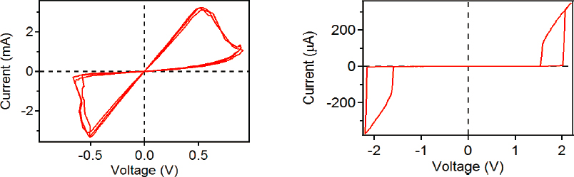
Williams explained two types of memristive devices of interest in computing. One type is nonvolatile and could be called “synaptic” because it shares properties of synapses with the ability to store the state or state variable as resistance in the device. This capability of nonvolatile memristors to store can be seen in the pinched hysteresis, or “bow-tie,” pattern of a trace of a voltage-current sweep, as shown on the left-hand side of Figure 2.1. This shows that when there is no applied voltage, the device may have at least two different values of conductance, which are represented by the slopes of the I versus V plot at I = 0 and V = 0. RRAM, phase change random-access memory (PC RAM), spin-transfer torque magnetic random-access memory (STT RAM), and other types of memory are all examples of this type of memristor. The RRAM version of these nonvolatile memristors tend to use materials such hafnium dioxide (HfO2) and tantalum pentoxide (Ta2O5) as the resistance change or data storage medium.
Another type of memristor exhibits locally active properties and could be called “neuronic.” As seen in the right-hand voltage sweep in Figure 2.1, there is only one conductance at V = 0 and I = 0; such devices transmit their state as a spike in voltage or current when a direct current or voltage is applied to the device. According to Williams, the spikes look and act just like the neuron spiking in brains, permitting transmission of information and performance of computation on that information via physical processes such as threshold switching, negative differential resistance (NDR), and Mott transitions. Locally active memristors can emulate neurons in
brains by replicating such important functions as threshold logic, and exhibit chaos. According to Williams, periodic and chaotic spiking behavior is important since it can enable highly efficient optimization routines, as further described below. Devices suitable for building locally active memristors can be based on Mott insulators, dielectric matrices with mobile ions, coupled redox reactions, charge density waves, and almost the entire palette of correlated electron materials.
Memristive Device Capabilities
Williams explained that one memristor implementation for computation acceleration is the crossbar, sometimes called a dot-product engine. In effect, a crossbar allows for customizable matrix operations, such as vector-matrix multiplication, in a single time step. Crossbars are constructed by connecting two sets of orthogonal wires by a memristor at each wire intersection. The conductance of each memristor can be tuned to a particular value by applying an appropriate voltage for a defined time across it, and in so doing create an analog representation of a real-valued matrix. Voltages applied to the rows of the crossbar represent the elements of an input vector, and each memristor performs a multiplication operation (current = voltage × conductance) by Ohm’s law. Each column of the crossbar collects all of the currents and conducts them to the bottom of the crossbar by Kirchhoff’s current law, where the sum of all the individual currents is measured. This process is a physics-based performance of a vector-matrix multiplication, and it occurs in one time step, almost independent of the size of the matrix (crossbar). This is an extremely fast and low energy way to perform computation, as long as the precision required for the result is within the bounds of the measured outputs.
Williams said that several groups have built crossbars to demonstrate their operability and capabilities, with some commercial products under development.
Researchers at Hewlett Packard Enterprise fabricated a simple crossbar that outperformed an optimized digital complementary metal-oxide-semiconductor (CMOS) system by a little more than one order of magnitude in terms of speed and efficiency when all of the digital-to-analog and analog-to-digital conversions were included. The Paul Prucnal research group at Princeton University compared the simulated ideal performance of their photonic system performing vector-matrix multiplication against optimized high-end digital systems and a memristor crossbar. Their simulation results showed that at 4 bits precision, the crossbar and photonic systems both outperformed the best digital system by at least four orders of magnitude, with the photonic system outperforming the crossbar by a factor of two. At 8 bits, however, the crossbar outperformed the photonic system by a factor of 16 both for energy and computing efficiency.
Williams also reported on results from Daniele Ielmini’s research group on dot-product engine crossbars solving reverse linear equations. This process applies currents across the bottom of the columns of the crossbar and then reads voltages from the rows once the system has reached steady state. This approach appears to function well independent of matrix size. The Ielmini research group has shown that this method can also solve first-order differential equations, find extremal eigenvectors, and compute inverse matrices. Moreover, these operations appear to be significantly faster and more scalable than similar operations on quantum computing systems.
Another example computing system mentioned by Williams is an electronic Hopfield network built by John Paul Strachan and collaborators at Hewlett Packard Enterprise, which has been applied to NP-hard (non-deterministic polynomial-time hardness) optimization problems such as “max-cut.” Optimization routines can become stuck in local minima when searching for the global minimum because they search stepwise from the current location by testing adjacent locations without the ability to see any more of the surface. This is like driving a car trying to find the lowest point in a mountain range when you can only see right in front of the car, have no map, and no ability to look around at the terrain. A common computational workaround is simulated annealing, which helps “bump” the system out of local minima (as if by patching holes in the road). This technique, however, is computationally expensive for digital computers. The electronic Hopfield network performs real physical annealing via the thermal noise in the hardware to get out of local extrema and continue searching for a global minimum. This system outperformed the D-Wave quantum annealer by 15 orders of magnitude in terms of the metric solutions per second per watt, primarily because it has a much higher connection “all-to-all” crossbar network and it operates at room temperature.
Materials and Dynamical Systems
Moving on to materials and dynamical systems, Williams recalled that memristors are defined axiomatically as a system described by a quasi-static conduction equation, or state-dependent Ohm’s law, and also by one or more dynamical equations that define the system evolution when the system is powered up. Some materials such as niobium dioxide (NbO2) exhibit volatile memristance, yet are stable at high temperatures, and have shown dynamical system characteristics when biased with current. Unlike many oxides that chemically decompose at moderate temperatures, NbO2 shows great thermal stability and a conductivity that varies significantly with both current and temperature. This provides a high degree of complexity and the display of current-controlled NDR—that is, the observation that the voltage across a device actually decreases over a finite range of increasing current. The system’s quasi-static conduction obeys the three-dimensional (3D) Frenkel-Poole tunneling process, which is thermally activated. As current flows through the device, its temperature increases because of Joule heating, which causes the conductance to increase. This results in a thermal runaway process that is moderated by Newton’s law of cooling, which states that hotter systems lose heat more rapidly. Thus, temperature becomes the state variable for the system, and the coupled equations for 3D Frenkel-Poole tunneling and Newton’s law of cooling result in the highly nonlinear and dynamical NDR, which creates the system’s volatile memory.
NbO2 and related materials also display Mott transitions, another type of nonlinear electronic instability. The Mott transition provides another physical mechanism for NDR. This additional complexity actually improves the value and utility of such a system.
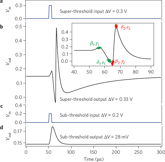
For instance, with two NbO2 memristors and two capacitors, Williams and colleagues built a four-state variable device that can emulate several properties of neurons. This so-called neuristor behaves like an “integrate and fire” pulse amplifier for threshold logic and communication. As seen in Figure 2.2, the spiking neuristor device was able to amplify voltage spikes just like a biological neuron, but three orders of magnitude faster and using just 1 percent of the energy that a brain neuron requires. This speed and energy efficiency arises because the system is all-electronic rather than a biological ionic system.
According to Williams, Wei Yi of HRL Laboratories, using vanadium oxide (VO2), expanded on this idea to build a range of neuristor-style devices. His team demonstrated experimentally that these devices could display all three classes of neuronal excitability and 23 out of 26 known biological functions. Each of these functions has a computational capability, making such devices computationally valuable.
In another example, Williams and collaborators from the University of Massachusetts, Amherst, demonstrated that diffusion of silver ions in silicon dioxide
(SiO2) or hafnium dioxide (HfO2) was facile enough to build diffusive memristors that function as analogs of synapses capable of performing simple computations. In another demonstration, the team used a diffusive silver-ion device that demonstrated potentiation. When utilized in a neural network, these devices demonstrated unsupervised learning.
Williams noted that Thirumalai Venkatesan and his colleagues at the National University of Singapore synthesized molecular materials that can change conductance in a device and are more stable than the inorganic oxides. These exhibit a transition based on system redox properties that produce nonvolatile storage superior to any yet seen for oxides in terms of endurance, stability, and reproducibility. It is also possible to build oscillators that demonstrate “integrate and fire” and potentiation, and at extraordinarily low energy requirements, in the attojoule regime. Such materials open a whole new category of system because they also demonstrate memcapacitance. This means that a single system will behave like two parallel devices: one able to remember resistance and the other able to remember
capacitance. With this combination, these materials will produce very interesting dynamical effects important for computation.
Oak Ridge National Laboratory (ORNL) researchers C. Patrick Collier, Joseph Najem, and colleagues built another memcapacitor in the form of a biomimetic membrane, essentially a proto-cell. The system’s physical flexibility provides memcapacitance because the device capacitance changes depending on the applied voltage. This may have noteworthy implications for neurobiology. The 70-year-old Hodgkin-Huxley model of a neuron assumes that neurons have fixed capacitance. Williams stated that the ORNL device suggests that this may not be true, and thus could require a significant revision in terms of understanding the generation and propagation of action potentials in living neurons. It also suggests that a wide range of sensors, detectors, and other devices could be built using biomimetic materials.
Williams said that with all these systems in mind, it bears returning to an application: optimization using chaotic systems. Materials like NbO2, for example, have enough degrees of freedom to display chaotic characteristics. Chaos disrupts synchrony, thus enabling higher-order functioning such as that displayed by the human brain. This permits symmetry breaking, system activation, and emergence of complex behavior.
Utility of Chaotic Properties
For instance, Williams said, with memristors, one can build a generalized crossbar that Leon Chua calls a cellular, nonlinear neural network. Setting a resistance in a nonvolatile memristor essentially installs a program. Sensors or other attached devices provide external inputs. A volatile memristor activates the system. It then evolves chaotically, always converging to an extremal end state. Convergence occurs, and quickly because the system is drawn to a strange attractor that imbues the ability to “see” more of the problem/optimization surface than other optimization routines.
To see how this works, Williams suggested considering a system comprised of a volcano sitting in a basin. The volcano’s cone features steeply pitched sides with a caldera roughly in the center. The lowest point is the bottom of the lava tube shaft at the center of the caldera, descending well below the basin. Thus, to find the very lowest point in the entire system requires looking, so to speak, at the very highest point. Traditional neural networks are unable to find this global minimum because their multidimensional minimization techniques search stepwise from the current location and strongly prefer to go down a steep slope. Rather than climbing to the top of the volcano cone’s slopes, such a routine will descend and settle in the basin. A completely stochastic search will eventually “fall” into the caldera, but this usually requires on the order of 1012 operations.
By comparison, the strange attractor in a cellular nonlinear neural network means that the search takes place above the surface, almost like hovering or flying. Moreover,
chaotic networks like this have an awareness that somewhere within it there are extrema, such as the global minimum in the caldera. The system always finds the minimum and at greatly reduced processing expenditure. The example here has never required more than 106 operations, and sometimes as few as 105, to find the bottom of the lava tube.
Discussion
Williams received two questions following his talk. One participant asked about the limits to oscillators, because energy dissipation and frequency determine their utility. Current materials, including NbO2, remain suboptimal, Williams noted. Even though the NbO2 neuristor required only 1 percent of the energy of a brain neuron to spike, there is still ample room for improvement. Creating new materials that allow finer tuning to specific areas will be valuable.
Another participant asked Williams to elaborate on the difference between the systems he described and molecular spin quantum systems. Williams stated that the main difference is the use of voltage and current as variables of interest instead of spin degree of freedom. The materials used, however, would allow for simultaneous use of all of these variables. For example, a system could be built using current, voltage, and spin, where spin could be utilized as a sensor or as a computational element.
RRAM: MECHANISMS OF OPERATION
Marek Skowronski, Carnegie Mellon University
According to Skowronski, traditional electronics relies on the motion of electrons. Resistive switching, on the other hand, utilizes the redistribution of ions in order to control the state of a device. The field of study investigating resistive switching is reflected in the name “iontronics,” used to describe circuits employing such effects. Skowronski noted that a search of “resistive switching” keywords in Web of Science will return nearly 8,000 results, and thus covering the mechanism of how different ions move through all of the materials currently under investigation is beyond the scope of a single presentation. Consequently, this section focuses on a subset of materials and phenomena—namely, binary oxides—used in the fabrication of RRAM.
Oxide-based memory devices are typically classified into three categories: valence change memory (VCM), thermochemical memory, and electrochemical memory. Each device is a type of nonvolatile memristor that stores information in the positions of atoms that, in turn, control the device resistance. Another feature common to all of these devices is the filamentary conduction, with current flowing along conductive paths formed within the device.
TABLE 2.1 Summary of Characteristics Classifying Two-Terminal Switching Devices (Memory)
| Valence Change Memory | Thermo-Chemical Memory | Electro-Chemical Memory |
|---|---|---|
| All are non-volatile. Change of resistance is due to redistribution of ions. Conduction is filamentary in large devices |
||
|
Mobile ions:
oxygen, exchange of oxygen with electrodes |
either metal or oxygen of the functional oxide |
mobile cations from the electrodes |
|
Type of switching:
bipolar |
unipolar |
bipolar |
|
Driving force:
electric field |
temperature |
electric field |
|
Temperature:
high |
high |
low |
SOURCE: Marek Skowronski, Carnegie Mellon University, presentation to the workshop.
The three types of memory device differ in terms of mobile ions involved in the process, polarity of switching, driving force, and operating temperature. Table 2.1 summarizes the characteristics of these three types of two-terminal switching devices.
Skowronski stated that the universal challenge for all memory types is the speed of writing and reading the information and its retention once written. The desire is for very fast writing, preferably accomplished in nanoseconds, coupled with very long storage time of 10 years or longer. The difficulty, however, is that an Einstein relationship binds the rate of ion motion induced by the electric field with the rate of concentration-gradient-driven diffusion, limiting the information retention. Materials in which ions move easily, thus permitting fast writing, exhibit shorter retention times. One strategy for meeting these apparently contradictory requirements is to increase the temperature during the switching process. At elevated temperatures, the mobility of ions increases exponentially, while at room temperature the diffusion is slow, allowing for long retention. However, the necessary temperature swing is approximately 1,000°C, causing a number of technical problems for switching devices.
Resistive switching devices reported in the literature, Skowronski said, even if confined to only the VCM-type based on binary oxides, show an exceedingly large variation in their characteristics. For instance, devices reported by Celano et al. in 20141 exhibited a filament with a diameter of about 1 nanometer that required
___________________
1 U. Celano, L. Goux, A. Belmonte, K. Opsomer, A. Franquet, A. Schulze, C. Detavernier, O. Richard, H. Bender, M. Jurczak, and W. Vandervorst, Three-dimensional observation of the conductive filament in nanoscaled resistive memory devices, Nano Letters 14:2401, 2014.
40 microwatts of power to switch between on and off states. By comparison, a widely cited 2010 paper by Kwon et al.2 used devices that had filament area 108 times larger, with 1,000 times higher power dissipation. It is quite clear that the operation of these devices must have been based on totally different phenomena and many reported characteristics are owing to excessive dissipated power and temperature.
Revising the Model of Filament Formation in Memristor Devices
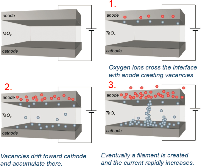
The initial model of resistive switching was proposed by Waser et al. and was briefly summarized by Skowronski. The as-fabricated devices are uniform in composition and conductivity. During the first application of a voltage sweep, the current initially increases gradually, but at the critical value of voltage, it suddenly jumps. This behavior was interpreted as due to gradual accumulation of oxygen vacancies in the oxide as the electric field forces the oxygen ions to cross the interface. Eventually, the oxygen vacancies pile up, forming a connection (filament) between the electrodes and the current jumps. This part of the process is referred to as “electroformation.” The model is illustrated in Figure 2.3.3
Once a device forms a permanent conducting path, switching relies on the redistribution of vacancies under the influence of an electric field. If a positive potential is applied to the top electrode of the device while it is in the low resistance ON state (corresponding to a continuous conducting filament), the oxygen vacancies will be pushed away from this electrode and create a gap and the high-resistance OFF state of the device. Reversing the field would close the gap and switch it back to the ON state.
Skowronski argued that the resistive switching process is much more complex than Waser’s model suggests. To start, the model has an obvious flaw. It assumes that both the current and the temperature in the unformed devices are low and that vacancies are mobile. If oxygen vacancies moved at room temperature, then the filament would dissolve by diffusion driven by the concentration gradient, meaning the device would not be able to retain the information once written.
New experimental evidence also necessitates multiple modifications to the Waser model. One way to see this is to add a series load resistor to the basic electroforming circuit. Monitoring the current during the voltage sweep (an I-V sweep) reveals an S-type negative-differential resistance (S-NDR) behavior, as seen in Figure 2.4(a), with part of the I-V exhibiting negative value of ∂I/∂V. Such I-V
___________________
2 D. Kwon, K. Kim, J. Jang, et al. Atomic structure of conducting nanofilaments in TiO2 resistive switching memory, Nature Nanotech 5:148-153, 2010, https://doi.org/10.1038/nnano.2009.456.
3 R. Waser, R. Dittmann, G. Staikov, and K. Szot, Redox-based resistive switching memories—Nanoionic mechanisms, prospects, and challenges, Advanced Materials 21(25-26):2632-2663, 2009.
characteristics in a circuit without load lead to an abrupt current jump once the voltage reached the threshold value. Upon lowering the voltage, the device returns to its original conductance, indicating no permanent changes to the structure and, hence, no ion motion. This phenomenon is known as threshold switching and is due to thermal runaway caused by temperature-dependent conductivity of an oxide.
An important characteristic of S-NDR-type I-V is a spontaneous current constriction. This characteristic is believed to be universal in all S-NDR-type devices. The extent of constriction was assessed by Skowronski’s team in collaboration with the National Institute of Standards and Technology (NIST). In the experiment, a tantalum oxide-based device was biased by a series of voltage pulses, which caused Joule heating and local thermal expansion. The team mapped the expansion as
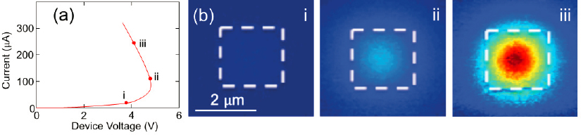
it increased the magnitude of the pulses. As the device moved deeper into NDR characteristics (from i to iii in Figure 3(a)), the conducting area constricted. This was visible in images obtained through scanning probe microscopy, detecting the deformation of the surface, as seen in Figure 2.4(b).
Rapid current increase and associated constriction leads to creation of a hot spot within the device with temperatures exceeding 1,000°C at moderate power dissipation. This sets the stage for the creation of a permanent conducting filament.
The red curve in Figure 2.5(a) shows forming I-V characteristics of a tantalum oxide (TaO2)-based device. The continuous line represents the initial volatile S-NDR dependence. One can retrace this part of the curve back and forth many times, provided the voltage sweeps are fast. By increasing the current to point B and beyond, the device is pushed into a region where permanent changes occur, as evidenced by the voltage returning to zero along a different path (dashed part of the red curve). The device has now become more conductive, likely due to formation of a permanent filament.
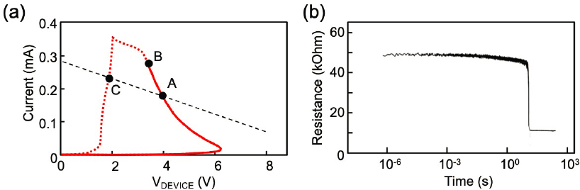
Skowronski said that another way to look at the formation process is to apply a long, constant voltage pulse and monitor the device’s resistance. The results are shown in Figure 2.5(b). The current increases to a steady-state value corresponding to point A in Figure 2.5(a) in approximately 1 µs (this corresponds to the thermal time constant of the structure used). After reaching saturation, resistance slowly decreases over ~10 seconds and then rapidly drops by a factor of 4. The slow decrease cannot be due to the changing temperature, because it takes orders of magnitude too long. Instead, the change is due to the diffusion process. As the atoms rearrange to form the conducting filament, the rate of motion is low at first. Changing composition, however, increases the conductivity and the current. This, in turn, increases the temperature, which speeds up the diffusion rate. At some point, this positive feedback loop between composition change and local temperature leads to a runaway similar to the one observed during the threshold switching part of the process. This implies that a device displays two successive runaway processes. First, during threshold switching, current rapidly increases because of the coupling between current and temperature. Then, current stabilizes for a time, but the high temperature allows for ions to move and results in a runaway process of composition change.
Two successive runaway processes present a challenge. Because these are highly nonlinear dynamical systems, very small changes in initial conditions can lead to very large changes in outcome. This means that the end product depends more on how the process is controlled—how it is slowed—than on the nature of the process itself. If the process is allowed to proceed rapidly—to run away—then the results become highly unpredictable. For instance, very small changes in testing protocols—for example, the value of the load resistor or the parasitic capacitance of the testing circuit—can result in very different end results in terms of device behavior and conductivity. This is true even in systems that are very similar at the outset.
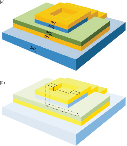
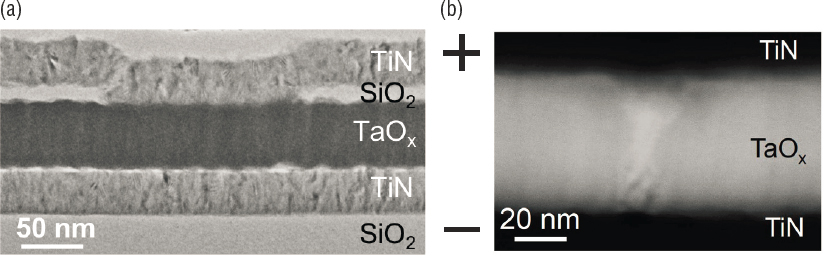
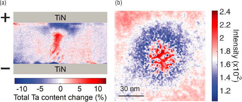
Skowronski stated that the structural changes occurring in the device during forming and switching have been revealed by scanning transmission electron microscopy (STEM) high-angle annular dark-field (HAADF) images. The device used in this experiment was a simple sandwich structure with titanium nitride (TiN) top and bottom electrodes (the gold color layers in Figure 2.6[a]) and the TaO2 functional layer (the green layer). For analysis, an electron transparent slab 2 × 5 × 0.05 µm in size was removed using focused ion beam (FIB) milling (Figure 2.6[b]). One can easily distinguish all layers in the device structure by looking at the bright-field transmission electron microscopy (TEM) image of a cross-section in Figure 2.7(a). The active area is defined by an opening in an insulating SiO2 layer, where the top TiN makes contact with the dark gray functional oxide. Lack of contrast in TaO2 indicates uniform distribution of tantalum.
After the device is formed, the TaOx layer shows a significant change in density, as seen in Figure 2.7(b). The brighter areas correspond to an increase in tantalum atoms, while the darker areas correspond to a decrease of tantalum content, as com-
pared to an average composition around the filament, which has stayed essentially unaffected. The image shows an accumulation of Ta ions forming a cylinder with a diameter of about 10 nm.
Finer features of the Ta distribution within the filament are easier to see in the false color maps shown in Figure 2.8. Only the middle 40 nm of TaOx layer is interpreted owing to 5 nm roughness of interfaces. The accumulation of Ta in the core of the filament is clearly visible as a red column in the center of the figure. In addition, the area at the top of the filament is depleted of Ta. According to Skowronski, this observation is consistent with the electrical characteristics of the device, which formed to the high-resistance state with a gap in the filament. Because the only source of Ta in the structure is the functional layer, the accumulation of Ta in the filament necessarily has to cause depletion elsewhere. Part of the depleted region is the gap at the top of the filament. This gap formed owing to the electric field forcing the positively charged Ta ions downward. The additional area of Ta depletion is shown in Figure 2.8(b); it is apparent that the tantalum ions have moved laterally into the center of the image, leaving behind a ring of tantalum-depleted area. The tantalum ions are moving and changing distribution much more than the oxygen ions are. This is unexpected and clearly contradicts the original VCM model of electroformation. Moreover, the lateral motion is perpendicular to the direction of the electric field in the device, indicating the presence of an additional force driving the ion motion. This force is caused by the temperature gradient, with elemental segregation induced by the thermal field referred to as thermophoresis, or the Soret effect.
The thermophoresis is known to cause a uniform AB alloy or a compound like TaO2 to segregate into A-rich and B-rich areas as one element migrates toward the
hotter areas and the other toward the cooler areas of the sample. The theory remains so nascent that it cannot predict which element will move in which direction and the experimental data are scarce. Nanometer-size resistive switching devices are highly unusual owing to their extraordinarily large, on the order of 109 to 1010 Kelvin per meter, temperature gradients.
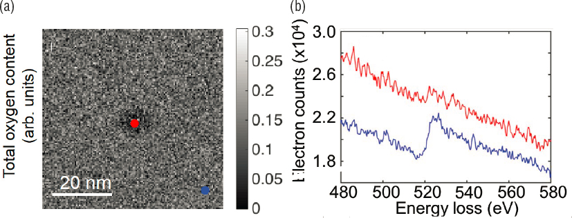
HAADF imaging can map out only heavy elements with O, N, and Ti contributing very little to scattering intensity. The oxygen distribution was assessed by electron energy loss spectroscopy (EELS), as can be seen in Figure 2.9. EELS does not have enough sensitivity to capture oxygen in cross-sectional views, but a plan view does show that areas that become rich in tantalum also show a loss of oxygen.
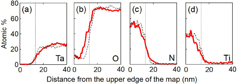
Skowronski notes that as the tantalum and oxygen ions redistribute inside the functional layer, it is interesting to ask whether the ions are interchanged between oxide and the TiN electrodes. A look at elemental line profiles obtained by X-ray energy dispersive spectroscopy (Figure 2.10) reveals that the distribution of all four elements across the interface with the anode is affected by electroformation and switching. Tantalum concentration at the top of the filament dips below that in a reference scan indicating creation of the gap. Oxygen concentration increases in the proximity of and within the TiN anode. The concentrations of N and Ti decrease within the TiN electrode and increase within the TaOx.
This is likely a product of interdiffusion, with the oxygen migrating after the tantalum begins to move and form the filament. For one, most of the voltage drop
occurs at the top of the filament, creating a temperature hot spot. The phenomena of electro- and thermomigration in devices at normal operating conditions discussed above are not unique to oxides and memristors. Phase-change materials (PCMs), such as alloys of germanium, antimony, and tellurium, also operate at high temperatures and extremely high temperature gradients. PCMs, when cycled, also demonstrate ion motion due to electric field, carrier wind, and thermal gradient. Segregation can be significant in as few as 10 switching cycles.
Unlike with metal oxides, this is an unwanted effect in PCMs because information is stored in the material structure, amorphous or crystalline, rather than chemical composition. Segregation affects the rate of switching, thus creating a big challenge for the PCM memory industry.
Iontronics and Storing Information in the Positions of Ions
A 2011 Nature Materials article from researchers at Samsung reported TaO2based resistive switching devices with extraordinarily high endurance of 1012 cycles, switching times of 10 ns, switching voltages between 1-6 V, and retention greater than 10 years.4 While this was a significant accomplishment, Skowronski noted that several characteristics still need to be improved.
Faster switching times are desirable, and some demonstrations with switching times as short as 100 ps have been reported. However, such experiments have used
___________________
4 M.-J. Lee, C.B. Lee, D. Lee, S.R. Lee, M. Change, J.H. Hur, Y.-B. Kim, et al., A fast, high-endurance and scalable non-volatile memory device made from asymmetric Ta2O5−x/TaO2−x bilayer structures, Nature Materials 10:625, 2011.
higher applied voltage and suffer higher dissipated power. Under those conditions, it will be challenging for the devices to have high endurance. More importantly, most devices demonstrated to date have the OFF resistances between 103 to 104 ohms while the large arrays require resistances on the order of 106 ohms.
Achieving this increase poses a significant materials challenge. The typical way to increase resistance is to decrease filament size. Filaments are already small, however, reaching the limit of single-atom width corresponding to quantum point contact regime where resistance is about 1.3 × 10⁴ ohms. The only way to increase the resistance further is to create a gap, but doing so means starting to lose control over resistance values. The variability of resistance becomes unacceptably large. This is a problem yet to be solved.
Endurance and Device Failures
Tested devices show the ability to endure between 106 and 1012 switching cycles, depending on test conditions. These are generally lower than the desired 1012 to 1014 cycles.
Multiple mechanisms appear to lead to failure, making it difficult to identify exactly why a device may fail. Devices that fail to the ON state show a decrease in resistance to low values. Likely this occurs because the prolonged switching causes the oxide to continually lose oxygen while the conducting filament grows in size or strength. Eventually, these processes go so far that the device cannot be switched off. The causes leading some devices to fail to the OFF (high-resistance) state is still not known.
Conclusions
In summation, Skowronski noted that resistance switching processes have proven more complex than initially thought. They are highly nonlinear, meaning that very small changes in structure or testing procedures can lead to highly different outcomes. The driving forces and processes responsible for the segregation, formation, and stability of the filaments remain poorly understood. Demonstrations of new devices frequently focus on a single feature such as switching speed or energy per switch, rather than a comprehensive evaluation of multiple parameters. In parallel, the concepts for circuits continue to evolve, rapidly changing the figures of merit for devices.
Discussion
Skowronski received and answered three questions. Raymundo Arroyave, from Texas A&M, attending in person in Washington, D.C., asked whether phase changes
could take place in the substrate or in composition changes from tantalum (IV) oxide to tantalum (V) oxide. Skronkowski responded that most of the active volume remains amorphous, although some crystallites can be seen forming at the hottest spot in the device, indicating some change from amorphous to crystalline solid. Locations where tantalum depletes and oxygen enriches have been observed to show the presence of tantalum (V) oxide even though the device is fabricated as uniform tantalum (IV) oxide.
An online attendee asked whether there is local charging in the filament associated with the composition change. Skowronski responded that it appears that the filament is electrically neutral, with the lower concentration of negatively charged oxygen ions compensated by lower positive charge of Ta ions. In the oxide as deposited oxide, Ta is present as either Ta+4 or Ta+5. In the filament, the charge state can range from +1 to +5.
Another online attendee asked whether oxide homogeneity plays a role in filament formation. Skowronski stated that it does. Several reports suggest that filament formation starts at the edges of the crossbar devices, where the thickness of the oxide is poorly controlled. This indicates the importance of physical deposition methods. Uniformity could be increased by using atomic layer deposition instead of physical vapor deposition methods. Nonetheless, Skowronski believes that even with a higher level of uniformity, all the processes described would still take place and device behavior would remain largely unaffected.
NEUROMORPHIC COMPUTING WITH POLYMERS
A. Alec Talin, Sandia National Laboratories
Talin began by stating that potential neuromorphic computing applications range from in-ear, real-time language translators to highly capable and functional autonomous vehicles to brain-machine interfaces. Constructing deep neural networks capable of substantially advancing these kinds of applications will require materials that can meet certain performance specifications. For instance, for such a network to have the level of trainability, accuracy, and energy efficiency required to be useful, the hardware should exhibit a high degree of linearity, a high density of analog states, and high endurance, and operate at low current requirements, ideally in the tens of nanoamps.
Development of organic materials for computing dates to at least the late 1960s, possibly earlier. Initially developed for potential nonvolatile memory applications, organic materials may also be quite suitable for memristors in neuromorphic applications. There is a wide range of materials with characteristics indicating potential for useful performance, including composite structures that form con-
ducting filament, polymers, and various molecular solids such as azo-aromatic metal complexes. Researchers have built many devices using these materials, including organic flash-style memory, transistors, and memristors that mimic synapses. Organic materials can already be seen in electronic applications such as electrochromics and organic LED (OLED) displays. There is some work on creating biological implementations in addition to broader neuromorphic ones.
Potential Applications of Neuromorphic Computing
Before providing details of the many materials under development, Talin noted that it is important to provide an overview of the potential applications of neuromorphic computing. Doing so provides a better understanding of the properties that materials must have to enable these applications.
Some potential applications include in-ear devices that instantly translate from one spoken language to a language the user can understand and autonomous vehicles with such high sensitivity and capability that they can recognize a cat in front of a car in time to avoid hitting it. These kinds of applications rely on edge computations, meaning that the processing of incoming data into actionable information is performed at the same location as where the data are being collected, not in the “cloud.” Doing so using deep neural networks (DNNs) executed on a digital platform is highly inefficient because DNNs require matrix operations that result in intensive shuttling of data between memory and logic. That requires a great amount of energy. Alternatively, DNNs executed on an analog platform, such as, for example, tunable nonvolatile memristive device arrays capable of both storing and processing information in the same location, can greatly increase energy and computational efficiency. The main properties required to achieve this are a high degree of linearity, analog nonvolatile states, high endurance, and low-current operation, ideally in the tens of nanoamps.
Materials Properties to Support Memristive Devices for Neuromorphic Computing
Talin noted that a DNN for optical character recognition can illustrate the need for key materials properties. Built from an array of synapse-mimicking memristive devices, this network would have an input layer that translates light intensity into proportional voltages. Those voltages would then be sent into the DNN, a complex layered network of artificial, memristor synapses. Before the DNN can be used for processing information (a process called inference), it is trained using relevant examples, such as hand-written digits. During training, these memristive devices would have had their conductances tuned so that as the voltages are applied from the input, a set of currents are produced as output from the first layer. A nonlinear
function, for example a sigmoidal function, determines whether the summed current is sufficient to propagate the signal to the next layer. This takes place down through the layers of the network. By comparing the actual output with the desired output (e.g., the correct identification of the digit) the synaptic weights are tuned using a process called backpropagation until the accuracy of the network reaches its maximum accuracy.
Training such a system to perform accurately and well requires tuning the memristors to the right values and developing a software regime to interpret the output. A high degree of device linearity is needed to avoid a small change in image brightness resulting in very large current changes. That situation would result in a lot of errors. Instead, an ohmic, highly linear device is desired, one that avoids extreme changes leading to values that get stuck on edges or extremes leading to errors. Talin said that this means avoiding large jumps in resistance or conductance.
There also is the issue of system current. Unlike digital CMOS computing, memristive devices do not depend on mobility of the carriers and should have low current. Keeping current low is essential, since useful device arrays will contain millions of memristive elements. Because the elemental currents sum for the device current, if each element requires microamps of current, the sum will be quite large. High current will lead to problems with electromigration and errors from voltage drops across the wiring between and among elements in the array. To avoid this, ideally current for each element should be tens of nanoamps.
Energy Efficiency During Training
A key way to produce a more energy-efficient network is to design it so that it undertakes learning and subsequent inference in parallel across the system. Parallel learning takes place when all weight adjustments in one direction, up or down, occur in simultaneous single steps. This means not needing to know resistance, conductance, or how much current or voltage to adjust. This can be done blindly, at least in some systems.
Organic Materials
According to Talin, the development of organic materials for computing started no later than the late 1960s, and possibly even earlier. One of the earliest examples was polydivinylbenzene films with lead electrodes at IBM. Likely that system formed filaments, although the researchers did not look for them. The aim of this particular material was nonvolatile memory rather than neuromorphic computing, although the characteristics resemble contemporary memristive devices based on inorganic materials. Another was copper tetracyanoquinodimethane (TCNQ).
Copper TCNQ exhibits electrical switching and memory phenomena. Investigators hypothesize that pi-orbital stacking allows for easier electron movement in one of two possible structural motifs that could be switched by application of sufficient electric field, though that is difficult to confirm empirically.
Investigators have also synthesized and investigated polymeric thin films. These are of interest because some support ion motion while displaying physical flexibility. This allows for wearable devices and other flexible electronics. Thin films also have potential for nonvolatile memory and can be so thin that they form filaments with quantum conductance. Device conductance is currently very high, however, presenting problems for neuromorphic applications.
Another class of organic materials demonstrating tremendous stability up to 1012 cycles are azo-aromatic metal-coordinated complexes. These have demonstrated close to ideal performance for read, write, and erase cycles, meaning that they have potential applications such as multistate memory. However, the fundamental mechanism and how to apply these effectively in analog neural networks remains unclear.
Talin stated that these complexes have multiple redox states, and the cyclic voltammetry shows that different redox states have different conductance likely because the coupling between constituent atoms is such that the presence of an electric field changes the kind of interaction required for electron movement. Though switching voltages were high in the initial prototype devices, they could be lowered by introducing gold nanoparticles to concentrate the electric field. Moreover, even though the device appears to have on the order of tens of distinct redox states, to be useful as a multistate memory it would need to have hundreds of such states.
In another instance, a nonvolatile polymer flash memory was built by stacking three different polymer films between electrodes that enable tunneling of electrons into traps. This changes the electric field so that the threshold voltage of the transistor changes. In this system, the well-known organic semiconductor polythiophine (P3HT) was interfaced against gold or nickel electrodes and a flexible substrate. On top of this, the researchers attached a layer of polystyrene or polyvinyl nitrate and then suspended gold nanoparticles between that layer and a ferroelectric polymer, letting them charge and discharge the nanoparticles. Although the voltages are still high, around 10 V, this is still an excellent representation of a flexible, organic flash memory.
Devices with Organic Materials
Talin noted that organic electrochemical transistors have been studied since the 1980s and continue to be the subject of extensive research. Unlike the materials with gold nanoparticles, these organic transistors can support a much larger number of states. These are bulk systems where charge states are part of the bulk of the
material, and thus they occur throughout the entire volume instead of just at the surface or interface. This allows shrinking dimensions while maintaining a high density of linear, analog states.
According to Talin, one system using PEDOT:PSS5 is a good example of a volumetric device. This device acts like a battery, but it could be used to store information instead of just charge or energy. The conducting channel is kept neutral overall even as the state of charge in the material changes, much like doping. This will change the conductance, depending on the state of charge.
Already in commercial use, electrochromics are another example of an organic material device that behaves very much like a battery. Electrochromics operate in a very similar way to organic electrochemical transistors, but even more like a battery. For example, the optical properties are changed by injecting electrons, or by removing electrons and injecting counterions.
An analogous system based on this idea modulates conductivity instead of optical absorption. Just like an electrochromic, it has two layers that each can store charge but instead of a continuous electrode, it has two electrodes that can measure electronic conductivity. The system is based on the volumetric change of redox state using PEDOT:PSS. The structure features two layers like the electrochromic devices. Both can store charge, like a battery. In this case, however, instead of having a continuous electrode along the bottom, the device uses two electrodes that can measure electronic activity, because the goal is to avoid voltage buildup.
Talin noted that mechanistic studies indicate that PEDOT:PSS devices behave much like a volumetric capacitor with charge stored between chains of positively charged PEDOT and negatively charged PSS. At the molecular level, rather than requiring thermal activation to build conducting filaments within the device, this system relies on removing electrons from the PEDOT so that it becomes positively charged while removing protons from PSS so that it becomes negatively charged. Because the strands tend to wind beside each other, the system now has some energy stored in an electric field between oppositely charged strands. Changing conductance is a matter of injecting or removing electrons (to PEDOT) and protons (to PSS). Because there is no need to build a filament, this is a relatively low energy process, requiring about half a millivolt. A 300 nm × 300 nm device is projected to require a switching energy of about 35 attojoules.
Plots of conductance versus number of pulses make clear that this device exhibits nonlinearity at the limits of its conductance range. As Talin stated earlier, a pure linear system is desired to avoid error. In this case, the nonlinearity is a result of part of the voltage dropping across the resistor placed in the electronic circuit connecting the gate and the channel to limit self-discharge. For very low resistance, the system requires less voltage to change the conductance state; however as soon
___________________
5 Poly(3,4-ethylenedioxythiophene) polystyrene sulfonate, perhaps the most studied polymer.
that occurs, the system would discharge through this low resistance and thus not retain the state. On the other hand, if the resistance is high, the state retention goes up, but at the cost of increased nonlinearity.
Returning to the desired device properties, to function well, a device should have very high resistance for storing information and very low resistance for writing information. One solution to create such a device with this system is to include a diffusive memristor in the circuit. Using this diffusive memristor instead of a limiting resistor improves linearity down to very low voltages.6 It does this because it can change resistance levels quite fast. The diffusive memristor forms silver filaments when a voltage of 150 to 400 mV is applied. When the voltage is removed, the atoms that formed the filament disperse back to the electrodes and the resistance increases very rapidly. This diffusive memristor switch will allow for low resistance to write and high resistance to store information. Storage with this device configuration can last for up to several days, which is long enough to undertake efficient in situ training because learned weights can be stored off-chip.
Parallel Inference and Training
A 3 × 3 array system based on this circuit with diffusive memristors that form silver filaments was used to undertake inference and, importantly, training in parallel. Theoretical results show that the past challenge of implementing memristors to train in an energy-efficient manner can be overcome. Simulations suggest that at 8-bit precision, such a system would show significant benefits over digital devices in terms of energy efficiency, latency, and chip area requirements.
Experimentally, it has been shown that a backpropagation training algorithm can be applied blindly, with the result that the system will tune the weights for memristor synapses until they converge. Using this information along with measured energy makes clear what properties matter most.
Synthetically Tunable Organic Materials
Synthetic tunability is one of the most attractive features of organic materials. For example, in the case of PEDOT:PSS, increasing the PSS fraction will increase the resistance. This happens because PSS functions like a dopant that enables ion transport in the PEDOT:PSS while also acting as an insulator. Adding more PSS creates a tunable insulating barrier. Experimentally, this has allowed tuning a system to perform at currents in the nanoamp regime with useful linear characteristics.
___________________
6 Talin commented that other devices may improve performance even more than the diffusive memristor, but he did not elaborate on their composition or specific performance.
Materials for Faster Switching
As Talin noted, fast switching remains an important property for any of these systems. Shrinking system size can allow quite fast switching. For instance, one system utilizing rapid proton transport displayed fast switching, as fast as a microsecond for devices of a few thousand square microns. Fast switching enables endurance testing, into billions of cycles without deterioration. Some recently fabricated materials can switch even faster, as fast as 20 ns, and the limit has not yet been reached. While such devices have not yet been fabricated to be well-sealed enough to prevent parasitic reactions, use of organic materials for other applications, such as the electrochromics and OLEDs mentioned earlier, suggests that this can be done for computing applications.
Materials Selection for Increased Resistance and Range
Additional characteristics of new organic materials can enable increased range of conductance and speed. For instance, in an electrochemical transistor, eliminating a different phase, like polystyrene, rather than having charge groups as part of the polymer increases performance. That increase translates into better performance, meaning greater range and faster switching in the material. The performance improvement is visible in experimental results.
Some potentially useful materials for room temperature proton electrolytes include ionogels. These are usually contained within polymeric or SiO2 walls. When spun on, the ionogel appears solid, but at the nanoscale it is still in a liquid state with high conductance.
In Situ Computing
In addition to the already-commercialized applications mentioned earlier, such as OLEDs, some of these memristor-type systems that could serve for neuromorphic computing are starting to be fabricated as integrated into silicon systems such as CMOS. One system build already consists of ionic transistors integrated into a CMOS chip that exhibited high algorithm benchmark performance.
Inorganic Materials
According to Talin, the most fundamental idea with inorganic materials is the same as with organics: to develop materials that can change charge state while maintaining the material itself as neutral, having as many charge centers per unit volume as possible. Talin suggests that we consider a battery: these store energy only and can be charged and discharged. Charging and discharging changes the battery
electrodes’ electronic properties, often beyond just the change in the Fermi level, as would be the case for doping silicon. This means that there will be transitions that can be useful for computing, such as Mott transitions.
Another system of lithium cobalt oxide showed a large change in conductivity indicative of a Mott transition. Because lithium cobalt oxide is a band insulator, when charging as a battery, the system moves lithium ions out, leaving behind positively charge polarons, positive poles that can conduct electricity. Along with a Mott transition and other changes, this system undergoes a large change in conductivity until it reaches an essentially metallic regime that enables highly linear changes in synaptic weights, and thus is useful for neuromorphic computing. Modeling suggests that this would exhibit high accuracy if implemented in a large network.
Lithium insertion into anatase to form LixTiO2, Talin said, shows linear behavior until a phase transition occurs at x ~ 0.2 resulting in coexistence of anatase and Li titanate phases. This transition can be observed in situ using Raman spectroscopy. Once the critical concentration of Li is reached, a second peak appears in the Raman spectra corresponding to Li titanate and coincident with a sharp drop in conductivity. This experiment was conducted at 80°C and demonstrated a subthreshold swing, or the voltage required to change the current by a decade, of 40 meV, well below the 60 meV theoretical limit for field effect transistors at room temperature. This is because the system is undergoing an electronic transition rather than trying to modulate a thermal distribution of electrons. This kind of transition could be very useful for neurons to compute integration and nonlinear functions as mentioned earlier.
The state changes in this system are the result of electronic and then lattice geometry shifts once lithium is introduced into TiO2. Initial introduction of lithium into anatase reduces a corresponding fraction of titanium ions from a +4 state to a +3 state. The extra electrons remain only loosely associated, forming a polaron. As more lithium is added, the electrons begin to fill 3d-orbitals in titanium, eventually having to go into degenerate orbitals. The natural abhorrence for degeneracy means that the system will rearrange—in this case, from a tetragonal to an orthorhombic structure—bringing about a large and useful change in conductance.
Talin said that many oxides exhibit this type of significant property change when charge is introduced or removed. This can be used to tune properties, often very quickly. As described earlier, they operate at low voltages and so tend to exhibit linear behavior (useful for synapses) as well as highly nonlinear characteristics useful for neurons, including durability, to millions of cycles without degradation. This idea shows promise, especially for implementing DNN. IBM has conducted some very promising work comparing these inorganic ion insertion systems to other technologies.
Metalorganic Frameworks
Metalorganic framework (MOF) materials are coordination polymers where redox-active organic ligands are coordinated to metal ions forming either a 3D or 2-dimensional (2D) framework. These materials have been the subject of investigation for several years. MOFs are structurally (not randomly) porous, with potentially a high density of redox states. Because the pores are regular and based on the structure and composition of the MOF, their chemical environment is controllable. This results in a great advantage for very rapid ion transport, changing charge state, and changing electronic conductivity.
One example of an electronically conducting MOF is the HKUST-1 infiltrated with TCNQ. TCNQ acts as a dopant, taking some charge out of the copper complex, thus enabling transport through this material. Prussian blue and its analogs are another examples of coordination polymers that could be attractive for neuromorphic computing. Analogs that replace iron with manganese or copper have shown ultrafast proton transport with useful conductivity that is very promising for neuromorphic applications.
The TCNQ@HKUST-1 and Prussian blue coordination polymers have significant three dimensionality. There are also several flatter, 2D semiconducting MOFs. For example, nickel HITP (2,3,6,7,10,11-hexaiminotriphenylene) can make thin film sheets. The HITP moiety coordinates to the metal ions. Copper and manganese work, in addition to nickel. This system is potentially attractive for rapid tuning of conductance by ion insertion and for independent optimization of ionic and electronic transport because the pores have been engineered so that they are perpendicular, allowing for more ion flow.
Biological Applications
Talin noted that these materials, particularly PEDOT:PSS, are particularly compelling because they have been used already in biological applications such as ion and neurotransmitter pumps. This makes them potentially ideal for connecting artificial intelligence computing devices with biological computing devices. They also have been used in sensing applications, by making transducers that change their electrical characteristics when exposed to a biological molecule such as dopamine or glutamate. This potential to connect to biological systems, use biological systems for computing, or improve the brain-machine interface makes these materials well worth continued investigation.
Discussion
Talin answered one question from an in-person audience member regarding whether peptides could be used with some of the materials discussed, particularly PEDOT:PSS, to improve the interface with neuronal or other brain tissue. According to Talin, this would likely be the case, but it probably depends on whatever biological element is the point of interface being able to change its environment, such as pH or electrochemical transmitter, and the ability to sense that change. These transistors have already been used for sensing at neural and other interfaces, such as heart or other muscles.
DEVICE REQUIREMENTS AND CHALLENGES OF MIXED-SIGNAL NEUROMORPHIC HARDWARE
Dmitri Strukov, University of California, Santa Barbara
Neural Network Models, Applications, and Digital Hardware
Although there are many different neural network models, such as deep convolutional network, liquid state machine, and deep belief network, all rely on very efficient implementation of vector-by-matrix multiplication. According to Strukov, this means that every neuron in the system must first compute a dot product before it can apply a specific function on top of that. As best as is currently understood, the only commercially used neural network models use firing-rate (nonspiking) feed-forward or recurrent network designs. Google employs the three most common designs in its data centers: multilayer perceptron, long/short-term memory, and deep convolutional neural network.
Strukov stated that the very largest and latest neural networks at the time of this workshop, such as attention networks,7 are used in natural language processing. These types of networks require an enormous number of weights to operate. Current state of the art is about 8 billion. They also require a very large number, over 1019, of floating-point operations. So only a few operation centers have the capability to train and operate this kind of network. It is also known that the larger the network, the better the quality.
As mentioned in prior sessions, to perform supervised classification tasks, networks first go through a training phase followed by an inference phase. In the training phase the network is trained to calculate the weights. In the inference phase the weights are unchanged, the same network is used repeatedly with different
___________________
7 Also called “transformer” networks.
inputs. The company NVIDIA has predicted that by 2020 inference would require more of the computing power than training, on the order of 4.5 × 10²⁰ integer operations per second. Likely the gap between inference and training will widen as Internet of Things technologies are adopted more widely.
With this in mind, Strukov said, it is important to consider how computing hardware for training and inference accelerators could be different. Training requires much higher precision but does not require persistence for weights. Furthermore, the weights usually keep changing during training, and hence volatile memory works. Training would be typically performed at cloud, so that a primary performance metric for the hardware is throughput per chip area. Inference would be more relevant for the edge devices with a primary metric of energy efficiency.
To undertake that level of computation, industry has developed specialized, high-performance processors that are very costly in terms of money and energy. Current examples include Google’s tensor processing units and NVIDIA’s Turing processors. Because of the cost and quick obsolescence, these may not be a good investment of public money.
Record performance for the digital processors is found in experimental digital systems. For instance, Cerberas has a physically very large chip, over 46 cm2, designed to work with large models that require a lot of memory. Performance of these systems is superior to commercially available systems, partly because of specialization, and also because of process node improvements. Although custom designs probably can continue to improve performance somewhat, their performance appears to be reaching saturation point and their costs are very high.
Moreover, said Strukov, these systems remain many orders of magnitude less energy efficient than biological (i.e., neurological) systems, because digital advanced processors expend most of their energy moving data. Static random access memory can be used as a proxy for on-chip data movement, and dynamic random access memory as off-chip. These large energy/latency requirements arise from computing using off-chip memory with bulky vector-by-matrix multiplication (VMM) circuitry—having to move information in and out of the chip.
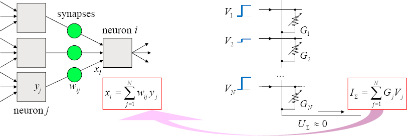
Neurocomputing with Memory Devices
Strukov stated that the main aim is to accelerate the basic operation: dot-product computation. Figure 2.11 shows an example of how to accelerate such basic operation: utilizing Ohm’s and Kirchoff’s laws to encode each of the input vector elements into amplitudes of voltages and the weights into conductances of the crosspoint devices, so that when the voltages are applied across the devices, the resulting current flowing out of the column is exactly the dot product. This means that the results are computed “in-memory” and there is no need to move weights around. Adding more columns with devices to the circuit on the right panel of
Figure 2.11, one can extend this concept to VMM naturally by extending input weights. While this is an old concept, until recently there were no dense adjustable-conductance nonvolatile devices.
Strukov mentioned two notable devices in the history of developing modern versions: Widrow’s memistor and the synaptic transistor developed by Carver Mead and his students. In the early 1960s Widrow’s group developed a three-terminal device, consisting of a metal wire (filament) submerged in electrolytic solution, where material was added or removed from a metallic filament via an electroplating process by applying the appropriate voltages to control wire conductance. A hardware was built based on such devices to implement image classification. Unfortunately for Widrow, his development of this device coincided with the rise of digital processors and waning interest in analog ones.
In the late 1980s Professor Carver Mead and his students developed a synaptic transistor. The concept involved implementation of floating-point gate transistor with traditional CMOS technology. This concept is still in use today in some impressive structures; however, synaptic transistors are very large in size and therefore quite area and energy inefficient.
New Life for an Old Concept
Strukov noted that many types of memories, memristors being one of them, are giving new life to this old concept. Several properties are essential for this concept: tunable conductance, nonvolatility, and extremely compact footprint. For example, for metal-oxide memristors, highly nonlinear switching dynamics allow for tunable conductance. Applying large voltages allows changing the conductance of the devices. Applying low voltages allows reading the conductive state while essentially leaving the device conductance unchanged. Furthermore, memristors can be used
to create very compact VMM structures because devices can be integrated in very dense structures.
In the most basic VMM structure, inputs are encoded into voltage amplitudes. One alternative configuration encodes inputs into duration of the fixed amplitude pulses and then integrates the charge at the output capacitor. Another applies inputs digitally, bit by bit, before integrating charge. The output circuitry calculates partial products to the specific kind of bit significance. Those partial products can be accumulated in analog fashion using the successive integration scaling technique or in digital fashion like in Hewlett Packard’s ISAAC concept.
There are pros and cons to each approach, Strukov said. To avoid drift in the conductance of memristors, smaller input voltages are required. However, small voltages lead to a smaller dynamic range for inputs and hence larger overhead of peripheral circuits. It also takes much more time to compute an output. For comparison, it would appear that biological systems are closer to the fixed amplitude, variable duration-type inputs.
Another recently proposed concept in the context of biologically inspired computing is approximate Content Addressable Memory (CAM), also known as hyperdimensional memory. CAM relates to VMM through its essential operation, calculating the Hamming distance. By definition, the Hamming distance is a dot product of two vectors. CAM performs this VMM operation with binary inputs and binary weights to compute an analog output. The largest output within the output vector is then chosen, and all other results are discarded. Understanding that the approximate CAM is essentially a VMM makes it easier to understand its advantages and disadvantages.
Memory Options
Resistive switching memories can be used in one of two kinds of memory arrays. Passive (“0T1R”) configurations use only a memory device in a memory cell. Active (“1T1R”) configurations couple each memory device with a transistor, which plays the role of a selector. While the density of 1T1R arrays is limited by that of transistor, the advantage is that in such a configuration many device requirements are relaxed. Figure 2.12 shows the prominent current memory options arranged in terms of maturity and cell density.
According to Strukov, the most promising in terms of density, at least in 2D versions, are the passive memristors, such as 2D CBRAM (conductive bridging RAM) and ReRAM (resistive RAM) positioned at the lower right corner of Figure 2.12, but they are also the least mature. There are also memristors used in active 1T1R configurations, such as active CBRAM and ReRAM. The most mature as of this presentation, said Strukov, is 2D NOR. One of the most intriguing is 3D NAND, because it already has such superior density to any other available options.
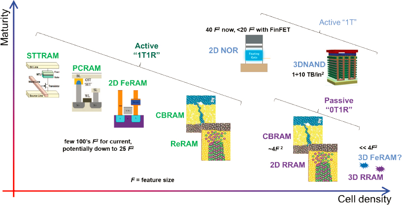
Last, to complete a memory discussion, is 3D FeRAM (ferroelectric RAM), which industry is heavily pursuing, and 3D RRAM. These are the least mature of all but hold promise of exhibiting the greatest density.
Inference Acceleration
Strukov said that ex situ-trained neuromorphic inference is perhaps the most useful benchmark for applications. A practical system must still be flexible enough to work with the many different types of networks. It must be designed to work with a mixed signal design. The main reason for this is to utilize weight reuse, a common feature of neural networks where they collect and temporarily store intermediate outputs. Digital domains are better suited for temporary storage, so the system should include circuitry for digital-to-analog and analog-to-digital conversions. Digital circuits are also necessary for exotic operations such as vector-by-vector outer product computations.
The University of California, Santa Barbara, developed a benchmark system for inference accelerators using its own architecture, called aCortex. The aCortex architecture is similar to other architecture in that its main component is VMM block with digital-to-analog conversion at the front end. The system calculates a VMM, sends the analog results to the neuron, which digitizes the result and sends it back to digital main memory. A controller orchestrates data movement from main memory to the VMM. Consequently, this aCortex is optimized for energy efficiency and less for throughput, favoring compactness over computing parallelism.
There are two useful things to note about this architecture. First, on benchmark testing it outperformed a digital CMOS counterpart, at the same accuracy and process node, in energy efficiency (TOp/J) and latency (ms) by four orders of magnitude. Second, the majority of the processor’s area is consumed by memory, but the energy is owing to moving this data across the chip’s buses, meaning that the energy is indirectly impacted by memory density.
In-memory computing density is a key enabler of this kind of technology. Another essential feature is analog tunability. When designing analog circuitry, it is common to overdesign with the expectation that the circuits must work in the worst-case process variations. The process variations become worse with scaling down feature sizes causing significant problems for analog circuits. This can be overcome at very low overhead cost, however, through conductance tunability. For example, an offset of the op-amps due to process variations can be compensated by adjusting device conductances, provided such offset can be properly characterized. Such a technique has been shown to require 30 times less energy in the peripheral circuits compared to a more generic analog design.
Trade-Off between Energy Efficiency and Throughput
There is also an important trade-off between energy efficiency and throughput. Strukov noted that this trade-off exists at different levels of abstractions (device, circuit, and architecture) in pretty much any computing applications. For inference computations the tradeoff mostly concerns peripheral circuitry. More peripheral circuitry (e.g., more analog to digital converters) is needed to increase throughput to perform more computations in parallel. The sparse circuitry, however, leads to larger distances to move data and hence worse energy efficiency but lowers throughput. By comparison, increasing the number of VMMs in parallel will increase throughput but requires more analog-to-digital converters, meaning more energy cost to run them.
This kind of natural trade-off can be seen in the qualitative log-scale plot of throughput versus energy efficiency shown in Figure 2.13. As seen in the figure, this suggests that the analog designs may be much better when energy efficiency matters, such as in edge applications, but there likely is some crossover, as precision or throughput matter more where digital is a better choice.
Strukov noted that it is important to benchmark systems properly. If possible, report system-level metrics. If those metrics are not available, then report chip-level metrics. For throughput, for example, metrics could be frames per second at a specified accuracy. For energy efficiency, the metrics would be energy per inference at a specified accuracy. Reporting in this manner ensures incorporating the range of details within the network, such as type of network, computing precision, type of hardware, and so on. As long as the Pareto front is pushed up, then there is some advancement.
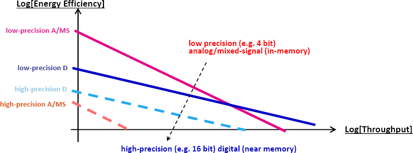
By comparison, secondary metrics such as TOp/s/cm2 or TOp/J must be used with care as they can be very misleading. For example, in a small network, TOp/J has little meaning since data is not moved around as far and as frequently as in a larger network.
Key Takeaways
The three key points in this section, according to Stukov, are as follows:
- Memristors are enabling elements for VMMs.
- Memristors can enable energy-efficiency increases of two orders of magnitude for inference accelerators because of their
- Compact footprint and tunability of passively integrated memristors; and
- “In-memory” computing within analog VMM circuits.
- Digital conversion impedes throughput and efficiency, although these conversions are necessary to take advantage of reusing weights.
Device Requirements and Challenges
Strukov stated that first, because of the need for tight integration with CMOS-based periphery, memristor-based systems must be CMOS compatible. Thus, memristors need to be conducive to back-end integration, and the voltage must be compatible with CMOS technology.
Second, device requirements and challenges are significantly impacted by the four major operations that memristors conduct in neuromorphic applications:
Forming, Write, Tuning Read (for ex situ tuning), and inference. Figure 2.14 illustrates the key device characteristics for these four operations.
Forming voltage to condition the crosspoint devices, is a very typical step in all the memristors. It is important to ensure that the voltage is low enough, closer to the read and write voltages, to prevent drawing large, potentially destructive currents through the already formed devices. For ex situ trained inference, weights are calculated ex situ, offline, in the computer, and then the conductance of each device is tuned individually using a write-verify algorithm. Strukov said that this requires applying a write pulse, then reading the results with a read pulse, then updating with another write pulse iteratively until hopefully convergence is reached to the desired conductance.
Two important consequences arise for neuromorphic inference accelerators due to ex situ training. First, metrics such as write speed, write energy, switching endurance, and switching dynamics will not be important. Inference applications do not require much programming of weights, so models need to be reloaded infrequently, as often as once per week or perhaps just once per month, meaning that weights do not need to be recomputed often once a system is deployed. Second, the write-verify algorithm allows for much greater device variation, because the write pulse amplitude adjusts through feedback for whatever variations are inherent in the device.
Inference requires devices with highly linear I-V because of the need for highly precise multiplication. This need for linearity is characterized by the ratio in the inequality I(VR)/(2I(VR/2)) > 0.95 for 4-bit precision. The memristors in use in these systems fortunately display high linearity at small voltages. Even a silicon photomultiplier diode at a few hundred millivolts will show significant linearity.
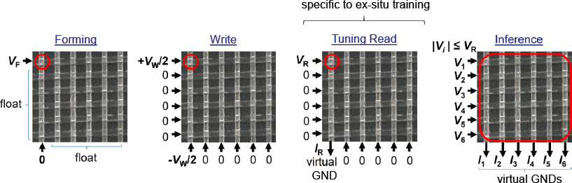
Major Challenges
Strukov noted that there are three major challenges. First, with the current state of the technology, there is a significant fraction of bad (i.e., not functioning properly) memory devices within systems. Coping with this requires providing redundancy. Currently, redundancy is provided through two mechanisms. One mechanism is to add spare columns and rows. Another is natural redundancy arising because of many zero weights in VMM kernels. With the first method, bad device areas can be eliminated through column-row redundancy, while the second method relies on mapping each kernel weight to the memory cell array so that bad devices coincide with weights of zero.
The fraction of bad devices that cannot be exceeded to ensure successful mapping is a function of VMM linear size. Crude calculations show that successful mapping for 128 × 128 weight kernels requires less than 1 percent of the bad devices for mapping with 95 percent success probability, even with relatively high ~60 percent row/column redundancy. It should be noted that if all bad devices could be characterized and incorporated into the training procedure via chip-in-the-loop or defect-aware ex situ training, a much higher tolerance could be achieved. This, however, has much lower viability for commercial applications because it requires “per-chip” training.
The second major challenge for the most prospective 0T1R arrays is that there are switching threshold variations also related to non-ideal devices in a system. When applying a voltage ramp across the device, at some point its conductance will change sharply. That jump is registered as a certain “switching threshold voltage.” Because of device variations, a distribution of such threshold voltages will be seen across a system of devices. The problem is that when applying a full bias across one crosspoint device, there will be some “half-selected” devices with only half of that bias. If the spread is large enough, it will disturb already-tuning half-selected devices. Avoiding disturbance requires a narrower distribution.
According to Strukov, the best weighting tuning precision and the methods for reducing weight precision without losing functional accuracy are still very much an evolving field. Vivienne Sze at MIT8 reviewed the accuracy of this image classification benchmark as a function of number of bits in the weight, and her conclusion was that they require between 5 and 9 bits of the weight precision. Implementing the most critical precision operations into the digital domain would probably allow 3 to 7 bits. In technical terms, tuning precision is defined as effectively 3 percent to 0.2 percent when defined as = 100% × |Gdesired – Gactual| / (Gmax – Gmin).
___________________
8 T. Yang and V. Sze, “Design Considerations for Efficient Deep Neural Networks on Processing-in-Memory Accelerators,” pp. 22.1.1-22.1.4 in 2019 IEEE International Electron Devices Meeting (IEDM), San Francisco, CA, 2019, doi: 10.1109/IEDM19573.2019.8993662.
The third major challenge is high cell currents. This challenge affects only memristors. High operating read current poses a problem because larger operating currents result in a smaller input/output array impedance, which leads to huge overhead for the peripheral circuit, such as the sensing and DAC circuits. Increasing the VMM array does not help much because the output currents increase with the linear VMM dimensions and hence DAC and sensing circuit overhead will also increase. The large write current is also a problem due to potential IR drop across electrodes, and especially for 1T1R arrays, because it swells the area of the select transistors.
In this context, a floating-gate transistor-like memory, such as NOR or NAND memories, have a big advantage. VMM circuits based on NOR or NAND memories operate in a sub-threshold regime with inputs applied to the gates of the transistors, leading to a much higher impedance and much lower overhead for that circuitry. There are also some advantages that can be gained for 1T1R concepts, to increase input impedance during inference operation.
The optimal current range at present is 100s pAs to 10s nAs. This range is accessible for flash memories because of the huge dynamic range of floating gate transistors in the sub-threshold regime. This range is chosen in a way that provides a high enough signal-to-noise ratio that the computing precision will not suffer, leaving 4 to 6 bits. Using lower currents will reduce computing precision.
Key Takeaways
The top two takeaways in this section are metrics and challenges, as follows:
- The most important metrics for the simplest, yet most practical neuromorphic inference applications are
- CMOS and crossbar compatibility;
- Density, especially for energy-efficiency optimal designs;
- Multilevel analog memory (4 ÷ 8 bits or 32 ÷ 256 states); and
- High retention, on the order of months. with negligible conductance drift (less then few percent).
- The biggest challenges are
- Poor device yield;
- Poor device I-V uniformity for 0T1R arrays (need <1% bad devices, sigma Vsw << Vsw/2), where Vsw is effective switching voltage; and
- High switching/operating currents (need hundreds of pAs to tens of nAs for operation).
Less critical than the first two takeaways are:
- Desired device specifications
- Dynamic/static I-V linearity;
- Write speed/energy;
- Endurance;
- Noise (random telegraph noise could be too high for some devices); and
- On/off ratio.
- Much more demanding device uniformity requirements for online/in situ learning—for example, spike neutral network with spike-timing dependent plasticity learning—although relaxed retention requirements for training accelerators.
Examples of Recent Mixed-Signal Neuromorphic Hardware Prototypes
In this section, Strukov provided information and operational details of several hardware prototypes characterized since roughly 2017. A very impressive chip from University of Michigan researchers features fully integrated 0T1R tungsten oxide memristors on top of CMOS. The chip featured 126 6 × 8 subarrays of passive memristor devices. The main weakness is that devices appeared to be volatile rather than nonvolatile, which may explain problems observed, such as poor minimum-scale retention and low complexity of demonstrations.
Strukov’s group produced a passive memristor 64 × 64 crossbar circuit. The fabrication approach is based on etch-down CMOS-compatible process allowing for low-resistance high-aspect ratio electrodes. The variations are low enough to precisely tune weights—for example, with about 3 percent tuning precision when setting weights according to the intensity of the pixels of the specific 64 × 64 gray-scale image.
Hewlett Packard Laboratories and University of Massachusetts researchers built the 128 × 64 active metal-oxide memristor array as integrated. This was the first fully integrated CMOS/1T1R HfO2 memristor chip of its kind. It was used in many impressive demonstrations, such as unsupervised learning, including for hardware and image compression. This system showed many positive characteristics, including very high (>99 percent) yield, linear I-V, and excellent analog properties. The cells are quite bulky, however, about 10,000 times larger than the basic memristor circuits shown earlier requiring high current (approximately 1 mA for the ON state).
Tsinghua University also built an active 1T1R memristor chip for neuromorphic computing. That chip was also a unique system featuring a tantalum bilayer with eight chips, each consisting of a 128 × 16 1T1R array of TiN/TaOx/HfOx/TiN devices board-integrated onto CMOS circuitry. The larger complexity allowed this group to demonstrate a convolutional neural network. Like the previous example, however, it is quite bulky, about 1,000 times the size physically of a basic passive memristive system that the University of California, Santa Barbara (UCSB), demonstrated.
UCSB also built a system using 2D NOR flash to perform neuromorphic inference. Strukov said that this is important because 2D NOR flash is a very mature technology. Most foundries have it in their process flow. The system implemented a modular architecture with 100,000 devices in 180 nm technology. It was trained to perform modified National Institute of Standards and Technology database (MNIST) classification through ex situ training. At the time, the experimental data showed that the system outperformed the best digital system, performing MNIST classification at the same accuracy by three orders of magnitude in terms of both energy efficiency and latency. It also showed no loss of classification accuracy after being left unpowered for 7 months. Current NOR memory systems of this type have been demonstrated in 55 nm process and show great promise for being a very accessible technology.
UCSB build another 64 × 64 crossbar system to solve optimization problems with a Hopfield network. Similar to what Williams showed earlier, this was in-memory computing circuits using intrinsic noise in the system to implement stochastic dot products or stochastic VMMs. To understand how this works, Strukov said, consider that a system whose signal-to-noise ratio is quite low, which could be achieved due to smaller utilized read voltages. The result of a dot product is fed into a digital comparator. Because of the intrinsic noise added on top of deterministic (or averaged over time) dot product value there is some probability that the voltage input will be larger than the comparator’s threshold and will be latched as digital one and, otherwise, some probability it will be latched as zero. A plot of those probabilities as a function of the averaged input to comparator will appear as a sigmoid curve.
The useful thing about this approach is that the slope of the sigmoid curve can be altered through dynamical changes to effective temperature by changing the applied voltage (and hence the signal-to-noise ratio). This feature is essential in restrictive Boltzmann machine, a variation of Hopfield network, which is especially suitable for solving combinatorial optimization problems. Tuning the weights requires significant time. Still, these networks can be practically used for solving very difficult, large-scale problems, which would be implemented on large networks. In those situations, the system would be set to different initial states to help it find better solutions after trying a large number of times. The systems based on the proposed stochastic dot-product circuits were estimated to have four orders of magnitude of superior energy efficiency and latency performance over competitive approaches.
Last, the UCSB group also conducted a purely theoretical simulation of a 3D NAND inference accelerator, which is suitable for large-scale neural network models. This test was pure simulation, unlike the other discussed examples of experimental or hybrid experimental and simulation tests, because at present these systems are available only from companies that want to keep the technology as a
business secret. The main feature is that they can implement VMM using a time-encoding approach without modifying the original 3D NAND structure. For the simulation, a 3D version of aCortex was developed. The main result is excellent area efficiency, meaning that this approach is suited for very large models. While it does not display the greatest energy efficiency, it is still quite high.
Key Takeaways
Strukov noted that the number of memristor prototypes being built shows the encouraging amount of progress that has been made. There still should be more variation in system types. It also bears noting that the more complex the system, the fewer the experimental data reported. The nature of the reported results should be put under scrutiny, because of sometimes misleading/confusing reporting.
Concluding Remarks
Strukov concluded that, in his opinion, for designing neuromorphic computing systems, it is important to consider whether all principles of brain operation are useful for designing computing hardware or algorithms. Many factors come into play for this consideration. First, for computing, the human brain does not appear fast. It is efficient only with tasks that help with survival, not a task like repeated addition. Even with many survival tasks, such as speech and image classification, machines can outperform humans on very well-defined benchmarks in very good contexts. More importantly, signal propagation in neural axons is many orders of magnitude lower and less energy efficient than in integrated circuits.
This raises the question of whether spike encoding is an artifact of brain evolution or a useful feature. It looks like an artifact because spikes cannot pass information, they diffuse right away, and they are a necessity in the brain rather than an important feature of the algorithm. Additionally, the brain exhibits huge variability tolerated by quite massive redundancy across both space and time. Massive redundancy naturally leads to only a small portion of neurons firing simultaneously—perhaps the cause of sparse encoding out of necessity rather than as a useful feature of superior algorithm.
This suggests that brain structure has arisen as the result of a fortunate fluke rather than as the best solution among different possibilities and that principles of brain operation are not all useful. Of course, the ultimate goal, human-intelligence algorithms, does not yet exist.
For these reasons, it seems likely that nonspiking machine learning and bio-inspired artificial intelligence efforts will both remain useful. Rather than discarding one in favor of another, probably hardware for machine learning and artificial intelligence will continue along two paths with overlapping hybrids. One path will
try approximate biology. This would involve things like efficient spiking hardware and could lead to breakthroughs in advanced artificial intelligence algorithms analogous to how graphics processing units helped lead to breakthroughs in deep learning. To this end, it is worth noting that spiking neural network hardware should be developed not because it is more energy efficient but because such hardware will help to more closely simulate the brain.
The other path will continue to focus on the more practical hardware side, continuing work on machine learning algorithms. This will lead to an interesting intersection of the two paths. For example, in a system with dynamic visual sensor cameras, spike encoding in the cameras could allow compression of 2D images sent to the periphery, while the backend would use some sort of nonspiking approach.
For all systems, there needs to be an efficient implementation of VMM. That will remain the most important operation.
Summary
In summary, Strukov said, neuromorphic inference with ex situ training is the natural entry-level application of mixed-signal neural networks. It is essential for all other applications, and it is the simplest in terms of device requirements yet is also practical. The technologies described here show at least two orders of magnitude of superior latency and energy-efficiency performance over purely digital systems for small-scale systems. Projections suggest that this will hold for bigger systems.
The most promising memory technologies in the long term are passive 3D memristors and 3D NAND, and in the short term embedded NOR flash and active 1T1R memristors. At present, these can accomplish a lot more than passive systems, because of the relaxed requirements for the memory devices.
The discussion centered around accelerating inference for the simplest type of neural networks. However, the potentials and the challenges of building inference accelerators would be also similar for many neuromorphic systems based on more advanced algorithms in which inference without training is useful—for example, in neuro-optimization systems that use stochastic neural networks or hybrid systems with spiking front-end dynamic vision sensor camera systems where inference without training is useful.
Discussion
Strukov received one question from Talin, who attended the presentation, regarding what has impeded industry from NOR flash in commercially available inference engines, given how ubiquitous this technology is and how easy it is to fabricate. Strukov responded that nothing is stopping industry. In fact, several
well-funded start-up companies are developing such systems. To do this, some of them licensed technology developed by Strukov’s group.
DEVICE ARCHITECTURES TO MEET NEUROMORPHIC COMPUTING CHALLENGES
Catherine Schuman, Oak Ridge National Laboratory
In this section, Schuman presented three important aspects of device architecture for neuromorphic computing. First, decisions made at lower levels of the computing stack, such as materials and devices (see Figure 2.15), produce significant and large impacts on higher levels such as algorithms and applications that influence the latter’s development. Second, careful thought about what can be done at the high levels can result in a co-design loop with the materials and devices levels. Last, there are opportunities to innovate with the materials and devices to influence the algorithms and applications.

Schuman proceeded with descriptions of developments at various levels in the computing stack, providing an overview of activity along with challenges and opportunities starting from the bottom of the stack. The section concludes with a consideration of the key challenge for ongoing development of neuromorphic computing and presents approaches to surmounting that challenge.
Materials and Devices for Neuromorphic Computing
According to Schuman, the basic performance functionality of a neuromorphic system depends on the materials and devices utilized. Decisions made at these levels influence all aspects of the computing stack.
In terms of decisions about materials to use, the earlier sections in this workshop provided significant detail regarding the spectrum of different materials employed to implement memristor devices, including artificial neurons and synapses. The spectrum includes heterojunction metal oxides, filamentary metal oxides, molybdenum disulfide (MoS2), graphene, nanoparticles, halide perovskite, polymers, and various biologically inspired materials.
Consider metal oxide memristors as one example. Selecting different materials results in significantly different device characteristics and behavior, such as the number and types of resistance states, switching speeds, endurance, stability, reliability, cost, and tenability. Those characteristics will have an impact on neuromorphic algorithms and applications, as illustrated in Table 2.2.
TABLE 2.2 Characteristics of Metal Oxide Memristor Materials
| Material | TE/BE | VSET/VRESET | Switching Speed | Retention Time | Endura nce |
|---|---|---|---|---|---|
| ZnO | Ag/Cu | 1.2V/-1.25V | - | - | >500 cycles |
| TiO2 | TiN/Pt | +1V/-1.5V | 1uS | 104 s | |
| LaO | ITO/SrTiO3 | 5V/-1.6V | - | >4x10⁴ s | 2000 cycles |
| TaOx | W/Pt | - | - | >10 years | 104 cycles |
| NiO | Pt/Pt | >10V/<-10V | - | >104 s | - |
SOURCE: Catherine Schuman, Oak Ridge National Laboratory, presentation to the workshop; data from B. Mohammad, M.A. Jaoude, V. Kumar, D.M.A. Homouz, H.A. Nahla, M. Al-Qutayri, and N. Christoforou, State of the art of metal oxide memristor devices, Nanotechnology Reviews 5(3):311-329, 2016.
Challenges and Opportunities with Memristive Materials
Schuman noted that challenges also present opportunities to innovate algorithms and applications. Consider the variability mentioned earlier from device to device and from cycle to cycle present in so many systems. These actually provide opportunities for algorithm development if algorithms can be built that can operate despite these variations and actually leverage them to improve performance. For instance, variation can help compensate for limited weight resolution as well as provide a source of stochasticity useful in some neural network implementations such as Hopfield networks.
On the other hand, variability may require retraining, or adaptation of algorithms to accommodate for the variations cycle to cycle or device to device, or perhaps on-chip training. As Strukov mentioned earlier, on-chip training to accommodate for the variation in the processes can lead to customizing every network to each individual chip, thereby curtailing commercial viability.
Limited weight resolution is another point of concern. The key disadvantage is that the limited resistance levels may limit the programmable weight values visible in the implemented neural networks. That can require changing the algorithm, using quantization and discretization approaches, for instance, to compensate for limited resolutions.
As with variability, however, there are advantages for algorithm development. In broad strokes, Schuman said, new materials create new computing behaviors. Algorithm designers can leverage those, creating new algorithms and applications. For example, there is some evidence to indicate that limited rate resolutions can benefit the generalization ability of the network. It appears that they can improve network performance as it takes in new data by limiting overfitting to the training data.
A more particular example is the work mentioned earlier with biomimetic synapses. Recall that at the device level, this has the appearance of two water droplets encased in lipids. The interface between the two forms a membrane. Hence, they are called droplet-interface bilayers (DIBs). Applying a voltage to the ion channel on one droplet causes it to open and allows it to function as a device. That behavior of the device closely resembles a chemical synapse in the brain.
DIBs provide an entirely new way to conceptualize synapse implementation with biologically relevant capabilities. They function as both a memristor and a memcapacitor. This allows them to exhibit a form of natural short-term plasticity quite similar to some short-term plasticity mechanisms in the brain such as pulse-paired facilitation and pulse-faired depression. Those plasticity mechanisms are uncommon in computing, and this appears to be the first device to have behaved in this way.
Because the DIB was a completely new device, Schuman said, it was uncertain whether it could provide any computational utility. Determining that has been the
domain of researchers at the architecture and algorithm levels of the stack. DIBs, then, exemplify both the impact that materials and device development can have on the rest of the compute stack and the importance of researchers at all levels staying abreast of developments at other levels and co-designing across levels, a point discussed in more depth below.
For DIBs, a research team at the University of Tennessee and at Oak Ridge National Laboratory implemented an analytical model characterizing the DIB behavior. They combined that model with models of solid-state and CMOS neurons to develop a software simulation of a neural network that performs electroencephalogram (EEG) classification, assessing whether an EEG signal is healthy or epileptic.
For this task, the network produces results comparable to other neuromorphic approaches. However, from Schuman’s perspective, this network is the smallest ever that has solved this task, down from tens of neurons and synapses to just six of each. As illustrated by the schematic in Figure 2.16, the structure is not in a typical layered format, but instead features recurrent connections from output back to the input neurons. This network design, and the algorithm to then perform EEG classification, was made possible by the fact that the materials’ properties appear to give rise to the network’s inherent pulse-paired facilitation and pulse-paired depression. Put simply, this is an example where materials’ properties appear to enable otherwise infeasible algorithms and network design that produce superior and more efficient outcomes.
Microarchitecture and System Architecture/Organization for Neuromorphic Computing
Architectures typically involve components implemented in CMOS, including CMOS neurons, although they may be memristive implementations especially for learning circuitry if the system will use on-chip learning or on-chip training. Architectural organization influences the algorithms and the applications, and thus it influences the types of network structures that can be implemented.
Earlier sections covered crossbars and the significant advantages that crossbar approaches provide, such as high density and low power requirements. Crossbars also suffer some potential disadvantages, however, such as potential limitations on achievable structures (the number of layers and recurrent connectivity, for example) and sneak paths updating memristor values, and they may not be well-suited to sparse structures. The DIB network to classify EEG signals, for instance, does not lend itself to a crossbar-based network.
Other architectures implement a neural core-based approach. In these networks, Schuman said, the neural cores are tiled and each contains a specific number of memristors and associates with one or more neurons. This approach offers more flexibility in the types of structures that can be realized and fewer idle components or unused computation for small, sparse networks. They also are less power and space efficient compared to a crossbar. Hybrid architectures with neural cores that are made up of tiled smaller crossbars provide some flexibility in realizable structures while offering some of the density and power efficiency of crossbars.
From the perspective of algorithms and applications, when building an architecture, how the system will be implemented and used must be taken into account. Deciding whether the structure should be optimized for a particular application or algorithm, or should be more dynamic to make it more usable across the neuromorphic computing field, is an important initial decision. Optimizing allows for a very fast, efficient system. It also can mean restriction to a particular algorithm type, or even a particular application. Building a dynamic, flexible system can provide more system usability, and allow use of more types of algorithms and applications, but at the expense of slower speeds and decreased efficiencies.
Algorithm designers try to look from both sides, noted Schuman, attempting to balance the desire for higher levels of dynamism and flexibility while also seeking as much application specificity as possible. This means attempting to build implementations that can optimize for accuracy, size, and energy. Including the additional objectives of minimizing energy usage and network size can halve energy usage and network size of an application-specific memristive circuit. Such a system would be very well suited to deployment at the edge in a situation requiring very low size, weight, and power.
Algorithms to Power Neuromorphic Computing
Key considerations for algorithmic development on neuromorphic hardware include the following:
- Realizable network structures for given hardware;
- Any reduced precision in the synaptic weights;
- Feasibility of on-chip training, chip-in-the-loop, or off-chip training performance;
- Dealing with noise, process variations, and cycle-to-cycle variation; and
- Hardware optimized for training or inference.
A paper co-authored by Schuman surveyed over 2,500 publications on neuromorphic computing and neural networks and hardware through early 2017. As evident from the chart in Figure 2.17, taken from that paper, by far the most common algorithm implemented on supervised systems is back-propagation, used to
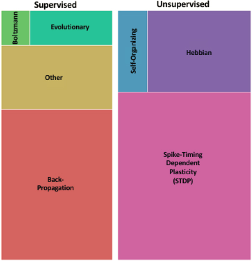
train deep-learning style networks, and on unsupervised spike-timing dependent plasticity, a particular type of learning mechanism detailed further below.
Back-propagation-like approaches have very dense connectivity characterized by layers fully connected to each other in the traditional machine learning program scenario. Low-precision versions require adaptations at the algorithm level, while increasing precision may require multiple memristors per synapse. As noted in the previous section, surmounting device variability may require on-chip training or chip in the loop.
Reservoir computing, sometimes called liquid state machine approaches, is a quite different algorithm. Reservoir computing is common for training spiking neural networks for neuromorphic systems because it relies largely on an untrained spiking neural network component as the reservoir connected to either a more typical kind of neural network as the training readout layer or some other readout layer component. The mix of different types of architectures suits this system well. It has very dense connectivity in the readout layer connected into different neurons in the reservoir. The system typically is fully connected yet may have sparse connectivity in the untrained reservoir that leaves it not as well suited for some of the architectures because the reservoir can have a lot of recurrence, cycles, and loops as a result of its network structure.
Reservoir computing algorithms have proven compelling for memristor-based implementations for a couple of reasons, said Schuman. First, this approach has demonstrated resilience to process variation noise, coping better than backpropagation-like approaches. It also benefits from the nonlinearity and memory characteristics of memristors. Because these algorithms map so well to memristive systems, it makes sense to build hardware that targets them.
Spike-timing dependent plasticity requires on-chip implementation of plasticity. Not only is it the most implemented learning mechanism on neuromorphic systems, it is also extremely common on memristive synapse implementations. Despite the high interest and level of implementation, the precise plasticity mechanisms remain poorly understood. For example, there is still little understanding of how to use this algorithm or what kind of network should be used to implement it. Given that, it seems that it should not be implemented as a stand-alone learning mechanism.
Application results at this point remain limited. Because its mechanisms are poorly understood, implementations such as Intel’s neuromorphic system Loihi allow for programmable plasticity. That enunciates a desire to avoid wedding to one specific plasticity mechanism, uncertainty regarding the best or correct plasticity mechanism, and a recognition that the most valuable option is to allow the user to define what plasticity should look like.
This aligns with the argument that the best plasticity mechanisms remain undetermined, and thus the best network structure to execute them. They may require
dynamic adaptation of the structure and the connectivity of the network, allowing for new connections to be formed between neurons in the system.
Evolutionary optimization algorithms address many issues associated with different types of hardware implementations, making them something of an intermediate approach to training neuromorphic systems. This approach often produces very small networks with very sparse connectivity. It produced the six neuron, six synapse EEG network discussed earlier. This approach can utilize chip in the loop without adapting the algorithm and help to accommodate for device and process variation. It will attempt to optimize within the characteristics of the device. This is a machine learning approach to devise a machine learning approach, meaning that it will use whatever resources are available to try to solve the problem.
For example, in the case of pulse-paired facilitation and pulse-paired depression that researchers do not yet know how to use, an evolutionary optimization algorithm will try to find a way to use it or at least optimize to operate in the face of whatever characteristics the device has. It can train for low precision, but it can be quite slow to train. Nonetheless, this algorithm has proven useful for exploring the capabilities of the different hardware implementations without having to write major algorithmic accommodations.
One implementation of an evolutionary approach, the Evolutionary Optimization for Neuromorphic Systems (EONS), can discover comparable performing networks within hardware constraints, such as weight precision or synaptic delay constraints. It will also optimize within the capabilities of the device (such as the biomimetic memristor, the DIB, discussed above).
Applications of Neuromorphic Computing
At the time of this presentation, Schuman noted, there appears to be a significant gap between what the neuromorphic computing community states are the most important applications and the most common applications. First, consider important hardware characteristics from an applications perspective, such as:
- Low power;
- Small/embeddable system size;
- Processing speed required;
- Robustness and resilience required;
- Integration with sensors and other compute; and
- On-chip training or learning.
Bearing this in mind, next consider that the most common application so far for neuromorphic computing and neural networks in hardware is image classification or processing followed by basic benchmark tests, very small-scale tasks like
evaluating a hardware circuit, as seen in Figure 2.18. By comparison, a survey of a large section of the neuromorphic computing community asking what characteristics of applications are best suited to neuromorphic computing systems produced the following list:
- Spatial-temporal;
- Noisy input;
- Realtime processing;
- Multimodal;
- Low power;
- Imprecise;
- Requiring robustness; and
- Continuous learning.
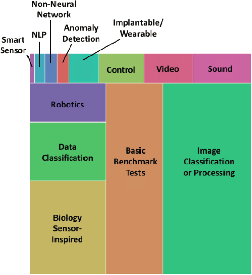
These characteristics poorly align with image processing or the simple tasks of benchmarking. Rather, they would seem better suited to applications such as:
- Scientific discovery;
- Coprocessing;
- Large-scale data analytics;
- Cyber security;
- Autonomous vehicles;
- Robotics;
- Internet of Things; and
- Smart sensors.
This list covers a wide range of applications and demands consideration that very different types of neuromorphic systems are going to be used in the coprocessor setting than for other applications.
More generally, when considering applications of neuromorphic computing, different levels of application will have very different application requirements. For example, large-scale models, faster than real-time processing, and fast retraining will be needed for cloud-level, data center, and high-performance applications. These systems likely will use different types of models or different types of algorithms, and they will need to be very flexible, whereas edge computing may focus on integrating information coming from many multimodal sensors and continuous “local” learning, not necessarily requiring retraining that cloud applications need. Internet of Things devices, sensors in the field, require extremely low power, high resiliency and robustness, and embedibility. They need to function well in extreme environments such as great depths underwater and high radiation, or when embedded, for example, in pacemakers or other health monitoring systems. They also need to be reliable for use in environments where they cannot be retrieved or replaced, such as on satellites.
The different levels of use also have different needs for optimization for training or inference performance. At the top, cloud-level, data center, and high performance applications will benefit from optimized training performance, while Internet of Things devices will benefit from optimized inference performance. Edge computing needs more of a balance.
An important pitfall to avoid is becoming locked into particular use cases that could limit innovation. The temptation with applications like processing, which have driven algorithms like deep learning, and, in turn, have influenced architectures like crossbars, is to optimize the algorithms and architecture for image processing. Following this route could create path dependency and stymie innovation. In reality, there should be innovative efforts at all levels of the compute stack to address the needs and potential of the many other algorithms and applications.
The Key Challenge in Neuromorphic Computing
Returning to the survey paper mentioned earlier, Schuman noted that the survey revealed that 73 percent of the neuromorphic hardware papers through January 2017 made no mention of an application and did not attempt to implement an application. This speaks to a key challenge in neuromorphic computing: a gap between communities of researchers investigating materials and devices and those designing applications that they know will benefit from neuromorphic designs.
Opportunity for Co-Design
Opportunity for co-design speaks to the opportunity for co-design between algorithms and applications and devices and materials, and between devices and materials and applications. For example, as noted earlier, the DIB biomolecular memristor has driven novel methods for learning at the algorithmic level. It provided new capabilities. Taking advantage of those new capabilities required algorithmic innovation, and there appears to be plenty of additional opportunity for algorithm improvement and innovation.
As illustrated in Figure 2.19, there is a valuable opportunity to utilize co-design between all levels of the compute stack—for instance, examining materials and taking inspiration from the capabilities already there in certain devices and materials and leveraging those at the algorithmic level, but also then providing requirements from the algorithms and driving innovation in devices and materials as well. As
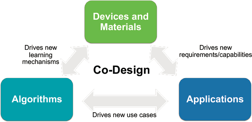
new materials are discovered and devices are invented, the door for innovation is opened for creating new applications that may otherwise not have been considered.
Schuman described an example effort to spur co-design found at the University of Tennessee and Oak Ridge National Laboratory (ORNL) called TENNLab. This collaborative has built a software framework to help bridge the gap between those conducting materials, devices, and architecture research, with the researchers and designers creating applications that they know will benefit from neuromorphic systems. The goal is to drive co-design to the benefit of the entire community.
The TENNLab system centers on a software core with common interfaces and learning engines it developed that integrate into hardware, or simulations of the hardware, spanning different types of neuromorphic hardware systems from fully digital systems like DANNA and Loihi, to metal oxide memristor-based systems like mrDANNA, DIBs, and optical electronic implementation. It includes many applications driven by real-world needs, such as static data classification, image recognition, temporal data classification (including the dynamic vision sensors mentioned earlier), event detection, and controls of interest for autonomous vehicles and robotics. TENNLab has applications implemented on different areas of real neuromorphic hardware and experimental hardware, to understand where the strengths and weaknesses of these systems are, and to close the loop on the co-design process.
One example of closing the loop is Schuman’s own work seeking to connect investigations of different machine learning mechanisms that define the neuromorphic systems found on neuromorphic computers with a search for understating how neuroscience inspired plasticity operates and how to use it effectively in neuromorphic applications. More generally, the goal is to combine machine learning approaches on high-performance computing systems and neuromorphic systems, simulating neuromorphic systems in different types of devices and materials on high-performance computers, along with real-world scientific data applications from user facilities like the Spallation neutron source at Oak Ridge, in order to discover novel ways of conducting unsupervised learning and new plasticity mechanisms inspired by neuroscience and also by the device materials that can be implemented practically in real-world neuromorphic systems for real-world applications.
Summary and Conclusions
In summary, Schuman noted that there is an important opportunity for materials research to inform the development of new algorithms. This should not be a unidirectional design process, with algorithms providing requirements down to the devices and materials. Rather, the opportunity is bidirectional. Algorithms should inform device and material design, and materials and device
discoveries should influence algorithm development because no one knows what the right algorithms are.
There is the need to develop hardware that enables the development and evaluation of new algorithms. As mentioned in the previous section, just as graphic processing unit (GPU) enabled much of the deep learning revolution, neuromorphic hardware will enable a spiking neural network revolution, which is much needed to accelerate the development of algorithms.
Last, hardware design should account for final application needs. Different applications and use cases have radically different needs. There is the opportunity for a vast landscape of different neuromorphic hardware implementations.
Discussion
Schuman answered six questions following her presentation, five from attendees at the live event, and one from an online attendee. Albert Wong from the National Science Foundation asked whether crossbars are used as a switch with controlled on-off or as an analog resister. Schuman responded that crossbars can be used both ways depending on the implementation. Wong also asked how the resistor values of a memristor can be controlled. Schuman replied that memristors do not have binary values but do have the option to be set at different levels. Moreover, different materials result in different levels of resistance states and thus resistance values. Cycle-to-cycle variability may exist in the actual implementation, meaning multistate values depend on material and device.
An online viewer asked for the distinction between the synaptic plasticity and the state variables emphasized by the earlier talks. Schuman replied that synaptic plasticity is a neuroscience-inspired approach for changing the weight value based on activity in the network. Those mechanisms have historically been inspired by activity seen in biological brains. Consequently, it is a function of the activity in the network, in spiking neural networks where the spikes are occurring, and is not a function of the device itself necessarily. It is a feature imposed on the device or architecture.
Sandra Lindo-Talin asked whether there is any consideration of ethics or social impact by the neuromorphic computing community. Schuman answered that this is a great question and points to a great need. The neuromorphic community thus far has not engaged very much. Of note, however, is that the artificial intelligence community has taken these on as huge areas of interest and has ties to the upper levels of the neuromorphic computing stack. The AI community continues to have many ongoing discussions and committees devoted entirely to developing adequate ethics for these systems. Hopefully, this will be translated to neuromorphic computing as well.
Minoj Kolel-Veetil from the Naval Research Laboratory asked what sort of materials should be used for particular applications, especially biological applica-
tions. Schuman has tried to maintain an agnostic stance to avoid prejudicial bias but imagines organic polymers would make sense for biological applications.
Raymundo Arroyave from Texas A&M University asked whether Schuman’s work focuses on attempting to develop evolutionary frameworks to find optimal arrangements between materials and implementations such as spiking or nonspiking. Schuman confirmed that is exactly the focus of her work.
FUTURE OF ENERGY-EFFICIENT COMPUTING BASED ON MEMRISTIVE ELEMENTS
John Paul Strachan, Hewlett Packard Laboratories
Examining the 70-year span from 1935 to 2005 of attempts to engineer intelligence, Strachan reveals a competition between two approaches: the connectionist and the symbolic. In simplistic terms, the connectionist approach models thinking as consisting of massively parallel simple functions distributed across bio-inspired networks. This would include the work of McCulloch-Pitts along with devices and approaches such as cybernetics with Norbert Wiener, perceptrons, Cognitron, neo-Cognitron, Hopfield networks, and deep learning. Again, in simplistic terms, the symbolic approach conceives of thinking as manipulating, or calculating, symbols, where symbols have both a physical/material reality and a semantic meaning, representation value.
A paper by Cardon et al.9 charts the timeline of the competition between the two approaches in terms of the ratio (log) of publishing citations referencing connectionist or symbolic approaches. Starting around 1995, the connectionist approach returned to domination. By 2020 many more connectionist developments had taken place, including recent progress in image video processing, speech to text, language translation, strategy games, and others. It appears, at this point in time, that the connectionist approach has triumphed.
Strachan noted that while many systems developed using symbolic approaches are still in use in very important computing systems, the ongoing dominance of connectionist approaches seems to have validated two things: first, a more brain-inspired—or neuromorphic—approach and, second, the need to emulate many more aspects of biological nervous systems.
___________________
9 D. Cardon, J.-P. Cointet, and A. Mazieres, Neurons spike back: The invention of inductive machines and the artificial intelligence controversy, Réseaux 36(211):173-220, 2018.
Significant Shift in Computing
According to Strachan, this signals an important and large shift in computing from programming (writing code) to architecting (building networks that will learn via examples). While there is a great amount of hype around deep learning, it cannot do everything. Many more breakthroughs must occur before computers replicate the capabilities of biological brains. Nonetheless, in reviewing developments over the past 85 years, it seems evident that while there is yet to be singularity, the computing community at least has decided on a cardinal direction for orienting effort. This is a substantial achievement.
Accelerated Increases of Computing Power, but Not Compute Efficiency
While these approaches have borrowed biological network topologies, they have not yet achieved compute efficiencies. The challenge this poses can be seen in the amount of training required for state-of-the-art neural networks, as compiled by OpenAI. Starting with the Perceptron in 1960 through to contemporary machines like AlphaGoZero, the compute used in the largest AI training run spans about 17 orders of magnitude. This demonstrates just how compute intensive these systems are.
Looking closely at the graph in Figure 2.20, two exponentially growing eras are evident. The first, from 1960 to 2012, tracks closely to Moore’s law, such that the compute required doubled approximately every 2 years. From 2012 to the present, however, the compute used for training has grown at an exponential rate, double about every 3.4 months—nearly a 12-fold increase per annum.
The current trend opens many questions about the future of research and development of next-generation networks. It is often stated that the types of networks explored are the ones that can be trained within about a week. This means the compute technology available sets a hard limit on research. For continued progress, and to avoid another “AI winter,” it is important to consider what improvements in hardware efficiency can be achieved.
Opportunities for Memristors and Neuromorphic Computing
Strachan said that there are also two opportunities for memristors and neuromorphic computing, as highlighted throughout the workshop’s presentations. One opportunity is to increase the energy efficiency of current artificial neural networks and deep networks utilizing in-memory computing and analog computing. While the neurons involved are not particularly sophisticated, a review of application numbers suggests that doing so would result in a 101- to 103-fold performance increase per watt of GPUs. These numbers arise from the work of many teams,
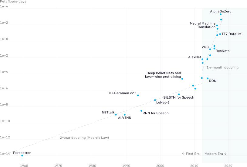
including Strachan’s, Strukov’s, Talin’s, IBM, University of Michigan, University of Dayton, Georgia Tech, and many more.
The other opportunity is to enable construction of more sophisticated brain-like neuromorphic elements. Most artificial neurons are built on simplified neuron and synapse models, such as the Hodgkin-Huxley model. Building upon models with greater similarity to biological neurons may be fruitful. So, too, could building new types of networks, like cellular neural nets.
Models of the Brain and Memristors
According to Strachan, Leon Chua makes the strong claim that brains are made of memristors. If this is true, then memristors may be necessary but not sufficient to construct brain-like systems. In 2012, Chua published a paper analyzing the 1952 Hodgkin-Huxley model of a neuron, a system of four differential equations with variable resistors, and elucidating an equivalent memristive model.
The Hodgkin-Huxley model itself has a very interesting feature. Mathematically, the model consists of a system of highly complex nonlinear differential equations. In the 1950s Hodgkin-Huxley and others investigated this model empirically, biased it at a certain operating point, and then fed voltage while monitoring current response. Under these conditions, they observed reactance in the system. It exhibited an effective inductance of roughly 20 Henries, quite large for a circuit of this size and type. This is 104 to 107 larger than commonly would be anticipated. In physical terms, 20 Henries is roughly a kilogram ferrite.
Interestingly, Chua’s work on the memristor equivalent is not about passive devices, Strachan said. This work is described not as small signal analysis but as a rich, complex system of differential equations describing a nanoscale device that displays analogous types of reactance and behavior, when studied in small-scale signal limits. As mentioned in the first section of this workshop, Williams and his colleagues have built a device and demonstrated that it can reproduce many of the behaviors described in the Hodgkin-Huxley model, while the HRL Laboratories team has developed memristor circuits that can reproduce 23 of the 26 known biological neuron spiking behaviors.
As described in the previous section, exactly how these devices will be useful remains to be discovered, but researchers are approaching their development from two different directions. If memristors can play a role in at least these two different ways, then it is really exciting that they are finally emerging. Foundries now offer high volume memristors in embedded memory products. This means wider availability beyond only a small number of device physicists with privileged access to lab-built memristors. Now circuit designers and computer architects can be involved in using these elements and initiate the virtuous cycle of designing, building, experimenting, characterizing, and iterating the cycle to improve design implementations. This should lead to an inflection point for memristor development and use in neuromorphic systems. This is essential to optimize, scale, and understand how to use and operate memristors.
Advantages of Memristors for a Range of Applications
Considering the three distinct properties of memristors—nonvolatility that enables in-memory computing, analog computing and tunability with large dynamic range, and nonlinear state dynamics—and treating each as a different characteristic, the Venn diagram in Figure 2.21 emerges, showing an interesting collection of likely applications to take advantage of memristors’ capabilities. Importantly, Strachan noted, many of these applications go beyond what are typically thought of as brain-like. Memristors, working within novel architectures, can improve or make possible broadly important applications with other architectures, across industry.