
I
Soldier Silent Power Challenges
As discussed in Chapter 5, “Dismounted Soldier and Light UAV/UGVs,” thermophotovoltaic power sources utilizing jet propellant 8 (JP8) present a major opportunity to reduce the weight burden of the dismounted soldier. Nevertheless, some technical challenges remain to be addressed before introduction onto the battlefield.
DEVELOPMENTS FOR TRL 6
Major development efforts are required to develop soldier silent power (SSP) to technology readiness level (TRL) 6. The cost of the program will be $1 million to $2 million and take 12–24 months for a feasibility demonstration in laboratory conditions, and an additional $2 million to $4 million and 12–24 months to deliver a fully functional and integrated prototype capable of operation under realistic conditions (a field experimentation). The areas of required development are outlined below.
INFRARED PV CELLS
Several companies are capable of producing high-performance indium gallium arsenide (InGaAs) on indium phosphide (InP) photovoltaic (PV) cells. Several fabrication-runs will be required to optimize performance in terms of open circuit voltage, fill factor, and quantum efficiency (ratio of incident photons to electrons at the terminals). The production runs will provide the cells necessary for system development and testing.
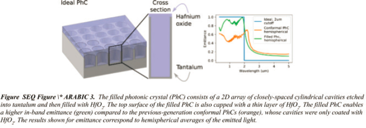
PHOTONIC CRYSTAL INTEGRATION
Photonic crystal integration has been demonstrated experimentally by the Army’s Institute for Soldier Nanotechnology at the Massachusetts Institute of Technology (MIT) in small planar systems.1 Two minor challenges remain for integration of photonic crystal emitters into larger cylindrical systems. The crystal emitter needs to be packaged in a vacuum (to prevent degradation by reaction with air) and the photonic crystal needs to be bonded to the micro-combustor:
- Mesodyne has developed a process for fabricating photonic crystals on flexible substrates that can be wrapped around and brazed to a cylindrical micro-combustor. A small amount of additional work is required to perfect the process.
- The vacuum package is an infrared (IR)-transparent (quartz or sapphire) tube that encapsulates the micro-combustor and photonic crystal, which optimizes the thermal band used by the PV to produce electricity. One end of the tube is sealed, and the other end is hermetically bonded to a metal tube for subsequent bonding to the micro-combustor. There are no commercial-off-the-shelf (COTS) products that match these requirements, although there are numerous companies that offer similar products and could custom fabricate the vacuum package. Additional development may be required to ensure long-term stability of the vacuum with the micro-combustor at operating temperature.
JP8 MICRO-COMBUSTOR
Numerous designs for JP8 combustors at larger scales exist, and several companies have developed burners in the approximate power range required for this project. The challenge is to integrate them with the novel thermophotovoltaic system, or alternatively modifying the existing microcombustor to be compatible with JP8.
JP8 combustion itself is not the primary challenge, rather it is vaporizing the fuel because it has a narrow temperature range between boiling and decomposition. Solutions exist, but the challenge is developing something that fits within the size and weight requirements of Soldier power to meet the future 7-day mission requirement.
___________________
1 W.R. Chan, V. Stelmakh, M. Ghebrebrhan, M. Soljacic, J.D. Joannopoulos, and I. Celanovic, 2017, Enabling efficient heat-to-electricity generation at the mesoscale, Energy and Environmental Science 10(6):1367–1371).
SYSTEM INTEGRATION AND MINIATURIZATION FOR TRL 7-8
This task covers the engineering work to transition from a laboratory prototype to a self-contained demonstration unit as follows:
- PV cell array packaging and cooling—design a lightweight heat sink and PV cell mount that keeps the cells cool and aligned with the emitter, while consuming minimal power with a small cooling fan.
- Control system—engineer a robust system to supply fuel and air to the microcombustor.
- Power electronics—interface between the PV cell array and the Soldier’s battery or power manager.
- Miniaturization—engineer all components to be compatible with a Soldier wearable solution. The microcombustor and heatsink will be the most challenging because the former needs to be a monolithic unit and the latter can be bulky.
- Housing—design a robust and ergonomic housing for the system.
In order to further improve efficiency and power density, the Army’s Institute for Soldier Nanotechnologies at MIT has developed a next-generation photonic crystal capable of omnidirectional emission approaching the blackbody limit for in-band wavelengths (see Figure I.1). This is accomplished by filling the cavities with a dielectric material and decoupling the physical and optical dimensions. Small samples have been fabricated by MIT, but a scalable fabrication
method compatible with standard semiconductor processes needs to be developed.
The numbers presented here are all based on the mature photonic crystal design from the Army’s Institute for Soldier Nanotechnologies at MIT. Maturing and adopting the filled cavity photonic crystal could improve the already very impressive bottom-line performance by an estimated 50 percent more.
DEVELOPMENTS FOR TRL 9
These efforts focus on manufacturability and production scale-up, ruggedization, etc. The cost of the program will be $5 million to $10 million and take 2-4 years for the first fieldable production run.
Photonic Crystal Fabrication Scaleup
This effort aims to mass produce the photonic crystal. A company, Mesodyne, has already eliminated a key bottleneck in the fabrication process—that is, removing wafer size limitations. Additional required development efforts include transitioning from small batches of small diameter wafers to large batches of large wafers, making the tantalum wafers compatible with non-academic cleanrooms. For example, by mounting the thin tantalum substrate on silicon wafers, and streamlining the process to eliminate the need for manual real-time adjustments to process parameters.
PV Cell Scaleup
This effort aims to mass produce the InGaAs PV cells. The primary barrier is the high cost of the indium phosphate (InP) substrate. At scale (10,000 wafers/month) the majority of the cost of the finished device is the substrate. Epitaxial liftoff, already developed for III-V solar PV cells, allows for multiple reuses of the same substrate, reducing cost by up to 70 percent. Additionally, the liftoff process will produce flexible cells, allowing for improved coupling to the cylindrical emitter.
Integration, Miniaturization, and Ruggedization
At this stage, the product can be designed for minimal weight and volume rather than ability to be built and modified rapidly. Additionally, the product will need to be ruggedized against drops and rough handling as well as dirt and water.
Design for Manufacturing
This effort covers manufacturing scaleup of the rest of the system. We do not anticipate major hurdles because every component has an analog that is already manufactured at scale.
Testing and Qualification
A significant amount of testing will be required to ensure the product meets performance, safety, and environmental standards. Additionally, user testing will ensure the product is easy to use in a battlefield environment.


