National Academies Press: OpenBook

The Physics of Materials: How Science Improves Our Lives (1997)

Chapter: 2 Technology in Daily Life

« Previous: 1 Introduction
Suggested Citation:"2 Technology in Daily Life." National Research Council. 1997. The Physics of Materials: How Science Improves Our Lives. Washington, DC: The National Academies Press. doi: 10.17226/9090.
×

2 Technology in Daily Life

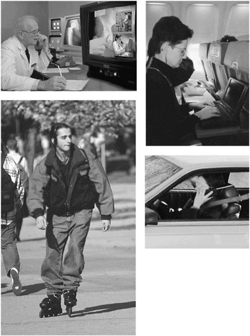
Here is a brief story about life today in the United States. It is fiction, but millions of episodes like it occur every day. Each event involves familiar technologies whose present state of development—or very existence— would have seemed extraordinary just a generation ago. The capitalized phrases in the story are links to sidebars on the facing pages that provide more information about some of these technologies.

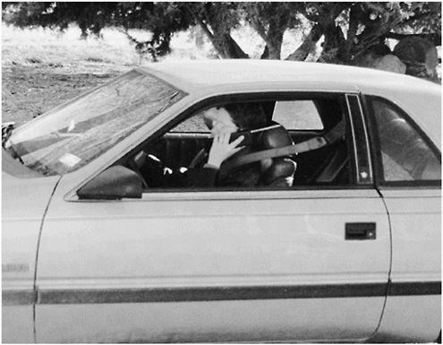
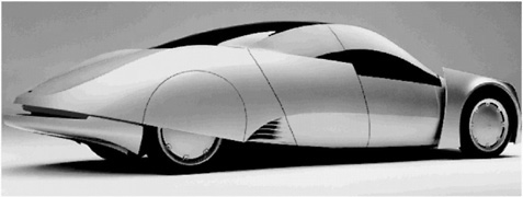
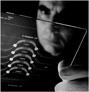
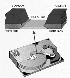
The owner of a small business is driving her car to the airport. Many structural elements of her car and the airplane that she will be boarding are products of research in MATERIALS SYNTHESIS. She is on the way to visit a potential customer. As a seasoned business traveler, she has with her all the tools she needs for her normal daily business. She picks up her cellular telephone and dials her son's pager. The communications revolution represented by the telephone and the pager has been greatly enhanced by advances in COMPOUND SEMICONDUCT ELECTRONICS.

Suggested Citation:"2 Technology in Daily Life." National Research Council. 1997. The Physics of Materials: How Science Improves Our Lives. Washington, DC: The National Academies Press. doi: 10.17226/9090.
×

MATERIALS SYNTHESIS

The materials in modern cars and airplanes that make them safer, lighter, and more fuel-efficient than their predecessors result from advances in materials synthesis and processing. Progress in the synthesis of materials takes many forms: research aimed at discovering new materials, development of methods for inexpensive and reliable production of such materials, incorporation of well-known materials in new geometries and environments, and continuous improvement of the production and processing of traditional materials. Each of these activities has firm roots in materials physics and chemistry.

“Nonequilibrium” materials processing involves raising the energy of the starting materals (for example, by heating) and guiding them into the desired final state. Such an approach has allowed the creation of new surface alloys that improve the wear characteristics of artificial joint replacements and machine tools. The opposite approach, operating very near equilibrium, is also useful. For example, it makes possible the growth of large, ultrapure, defect-free crystals of silicon for use in the semiconductor industry.

The production of traditional materials also continues to evolve. An object as simple as an aluminum can is a good example.The raw material these days consists increasingly of recycled cans. Can walls are being made thinner and thinner, an achievement made possible by close control of the alloy composition and of the processing of the aluminum sheet. Optimization of these processes increasingly requires integration of computer-based modeling over a large range of length scales: from atomic bonds, motion of dislocations, and deformation and rotation of individual crystallites, to macroscopic behavior.

Another example is the development of alloys for jet aircraft. Alloys in early jets suffered from fatigue that ultimately led to disintegration. Modern alloys are not only stronger and lighter but also more resistant to stress.

FIGURE 2.1 A futuristic high-performance aluminum car. (Courtesy of Ford Motor Company.)

COMPOUND SEMICONDUCTOR ELECTRONICS

Silicon is the material underlying most electronics, but compound semiconductors composed of more than one element, such as gallium arsenide (GaAs) and silicon germanium (SiGe), have advantages that can lead to devices with intrinsically higher speed and lower noise. The worldwide market for compound semiconductors is estimated to be $750 million in 1996, and it is growing at the rate of 40% per year. Discrete components are now widely used in the low-noise receivers of cellular telephone handsets, in addition to the specialized high-speed microwave applications for which they have long been the materials of choice.

FIGURE 2.2 A high electron-mobility transistor (HEMT) such as those used in cellular telephones. The round bonding pads are 100 microns in diameter, roughly the size of a human hair. The gate of the transistor, just 0.05 microns across, appears as the two narrow lines in the center of this scanning electron micrograph. (Courtesy of Sandia National Laboratories.)

Compound semiconductors such as GaAs, SiGe, and gallium nitride (GaN) are key to the development of the next generation of wireless telephones, which will use higher frequency microwaves in order to transmit more information. GaN transistors, for example, are characterized by high breakdown voltage and great robustness. A potential high-volume application for such transistors is in transmitter power amplifiers for wireless base stations.

Pushing the limits of semiconductor materials technology is essential for increasing the speed of transistors and advancing our ability to modulate lasers for high-speed optical information transmission. Because compound semiconductors are composed of more than one element, they promise a vastly increased range of materials from which to select those with desired electronic properties. This promise can be realized with manufacturing techniques such as molecular beam epitaxy, which allows the repeated, controlled, precise growth of one material on another in single atomic layers, producing compound layered materials not seen in nature. In the future, the use of novel forms of microscopy for fabrication and testing will determine our ability to design and build such structures on the atomic scale— a scale on which the motion of electrons is governed by quantum mechanics.

Suggested Citation:"2 Technology in Daily Life." National Research Council. 1997. The Physics of Materials: How Science Improves Our Lives. Washington, DC: The National Academies Press. doi: 10.17226/9090.
×

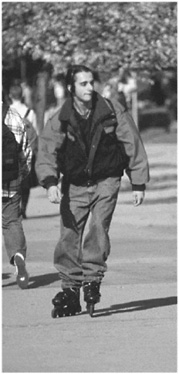
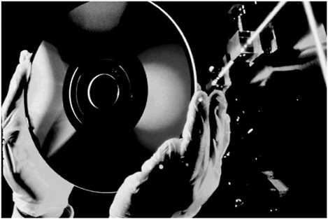
The woman's son is a college student who, at that moment, is rollerblading across the campus, listening to a compact disk that he has just recorded in his music course. His rollerblades are light and strong and run smoothly because of advances in the physics and chemistry of POLYMERS. The compact disk, containing over an hour of high-fidelity music, is a miracle in the development of OPTICAL STORAGE MATERIALS. The crucial component of the student's portable CD player is a SEMICONDUCTOR LASER.

POLYMERS

Polymers permeate our lives, from the new, lightweight materials that improve the fuel efficiency of cars and airplanes to the high-strength components that make possible in-line skates and other sporting equipment. Polymers are molecules composed of many molecular units (“mers”) connected together into macromolecules. A single polymer macromolecule may consist of a million or more atoms. Chemists have learned how to make an almost endless variety of highly complex yet well-defined macromolecules that incorporate a wide variety of monomers. Today, significant improvements in chemical synthesis and a growing collaborative effort between polymer chemists and materials scientists have resulted in the availability of extremely well-defined materials with novel properties. Given the sophistication of current polymer synthesis, it is now possible to systematically test hypotheses about how a polymer's properties are related to its structure and to design macromolecules to form specified microstructures and provide desired physical properties.

Some people still think of polymers as weak and flimsy compared with metals and ceramics, but in fact, truly impressive physical properties have been achieved. Some polymers are 1.5 to 2 times stronger than steel, and because their densities are typically only one-fifth that of steel, this means 10 times greater tensile performance per unit weight! The polymer Kevlar is used in bulletproof vests.

FIGURE 2.3 This false-color micrograph shows the structure of a block copolymer. The orange and yellow regions contain disordered chains of small, chemically distinct units (here denoted A and B—many different substances can be used) that are strung together in sequence AAAABBBB. . . . If the B substance (yellow) is chosen to be soft and rubbery while A (orange) is hard and glassy, adjusting the A-to-B ratio permits production of copolymer materials with a wide range of mechanical properties. Such materials are very inexpensive to process, because the array of A and B domains forms naturally. One application is in the soles of high-tech running shoes. The scale bar is 100 nm (10−7 m) long. (Courtesy of Cornell University.)

Suggested Citation:"2 Technology in Daily Life." National Research Council. 1997. The Physics of Materials: How Science Improves Our Lives. Washington, DC: The National Academies Press. doi: 10.17226/9090.
×

OPTICAL STORAGE MATERIALS

The compact disk in a CD player is the most common example of optical storage, an industry with $8 billion in annual sales. Information is stored on a CD in the form of shallow pits just a few thousand atoms across. These pits are embossed in a polymer surface coated with a thin reflective film, and the digital information, represented by the position and length of the pits, is read optically with a focused laser beam. The same format is also used to store information on a computer—an encyclopedia, for example, or a piece of software — in which case it is called a CD-ROM (compact disk read-only memory).

Many materials challenges had to be surmounted to make this technology possible. The availability of inexpensive semiconductor lasers made it possible to read the disk. Substrate materials had to be invented with the optical, mechanical, and chemical stability to ensure reliability and long life. A manufacturing process had to be developed that could produce high yields of reproducible patterns with small features.

A future challenge is making optical storage erasable so that CDs can be used in the same way that we use memory devices in computers. Two approaches are being studied; both rely on improved materials. One uses light to locally change the direction of a material's magnetization, which can then be read out by detecting its effect on the polarization of another beam of light. The other uses a laser to change the local arrangement of atoms in a material, altering its reflectivity.

FIGURE 2.4 A magneto-optical disk. Information is stored magnetically and read out optically. (Courtesy of IBM Research.)

SEMICONDUCTOR LASERS

Stimulated emission of light, the physical principle that underlies all lasers, was predicted by Albert Einstein in 1917, but it was not until 1960 that the first working laser was developed, using ruby crystals. (A microwave version known as a maser was built in 1953.) Within five years came a variety of other important developments: laser spectroscopy, the use of lasers for telecommunications, the carbon dioxide laser, and the semiconductor laser.

Semiconductor lasers made the photonics revolution possible. For example, they produce the beams of light used for transmitting information and reading compact disks in a CD player. Lasers made of the semiconductor gallium arsenide (GaAs) can emit light particularly efficiently because of GaAs's electronic structure. In addition, it is possible to combine GaAs and related compounds to tailor the optical properties and vary the color of the emitted light. Under favorable circumstances, nearly perfect single-crystal growth (epitaxy) of layered structures of different semiconductors is possible. This allows fabrication of miniature, continuously operating lasers the size of a grain of salt. Such lasers today find wide application in such diverse areas as telecommunications, laser printing, bar code recording, medicine, and video and audio disks. Nearly 50 million semiconductor lasers are now sold annually.

FIGURE 2.5 Blue Light emission from a gallium nitride semiconductor LED. (Courtesy of the University of California, Santa Barbara.)

More than 20 billion closely related light-emitting diodes (LEDs) based on the same materials technology are sold each year—enough for 3 to 5 for every person on Earth! With new materials and careful tailoring of the optical properties using advanced crystal growth techniques, lasers can be produced that span the spectrum from medium infrared wavelengths to visible light, including green and blue. Such advances hold new promise for military and space communications, for optical recording and display, and even for longer-lived, more efficient, and more reliable traffic lights.

Suggested Citation:"2 Technology in Daily Life." National Research Council. 1997. The Physics of Materials: How Science Improves Our Lives. Washington, DC: The National Academies Press. doi: 10.17226/9090.
×

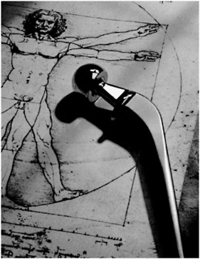
Feeling the vibration of his pager, the student turns off his CD player and hurries to his dorm room to return his mother's call. The message is about his grandmother, who has been hospitalized following an accident. A CAT scan has indicated that she needs a hip replacement. Artificial bone replacements are possible because of research in BIOMATERIALS.

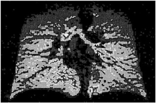
Fortunately, an additional MRI scan has ruled out any spinal injury. Magnetic resonance imaging (MRI) depends on SUPERCONDUCTING MAGNETS.

The attending physician believes that the surgery may be more complex than usual, so he has arranged a video consultation with a specialist in another part of the country before operating. Videoconsultation is an example of today's growing use of OPTICAL FIBERS for telecommunication.

The surgery has been successful, and the patient is resting comfortably.

BIOMATERIALS

Special-purpose metal alloys and polymer coatings are used to prevent the body from rejecting prosthetic bone replacements. Many other new materials are also used in medical applications where they must stick to bone, mimic color, flex like natural tissues, and keep their form under extremes of heat and cold. The secret in making an artificial material compatible with living substances is in discovering the ways of “soft condensed matter,” the plastic materials that act neither as solids nor liquids, whose properties can be modulated by a combination of chemical synthesis and physical treatment.

The next time you have a front tooth filled, notice the range of colors and textures that the dentist is able to create to match that of your particular tooth. Watch how he or she mixes a sticky putty to fill the space, smooths its surface, and applies ultraviolet light to cure the putty into a lump of just the right flexibility and tenacity. What is going on? A mixture of entangled, space-filling polymers flows nicely into the clean cavity. The ultraviolet light drives chemical reactions between the polymer molecules to harden them into place. The whole operation takes only a few minutes, and the full setting takes only hours. A new material has been created right in your mouth.

It is no surprise that these new procedures are coming into use at the same time that we are learning so much about the physics of polymers —how they flow, how they mix, how they stick, how they pack. These have been subjects of intense study, driven by the physicist's desire to explain surprises not seen in traditional solids and liquids and by the chemist's joy in creating materials with novel properties.

FIGURE 2.6 An artificial hip joint made from a special-purpose surgical alloy and processed by ion implantation to reduce corrosion and wear. Approximately 200,000 hip replacements are performed in the United States each year. (Courtesy of Oak Ridge National Laboratory.)

Suggested Citation:"2 Technology in Daily Life." National Research Council. 1997. The Physics of Materials: How Science Improves Our Lives. Washington, DC: The National Academies Press. doi: 10.17226/9090.
×

SUPERCONDUCTING MAGNETS

Nuclear magnetic resonance, the basis of magnetic resonance imaging (MRI),was invented to study the local environment of atoms in matter. With the development of high-speed computers and advances in fundamental mathematics, it is now possible to make high-resolution images using this technique. Making such images requires placing the subject in a strong magnetic field, typically provided by a superconducting magnet.

When certain metals are cooled to low enough temperatures, they pass into a superconducting state in which electrical currents flow with no resistance. A current flowing in a closed loop of superconducting wire will flow literally forever. Many useful scientific instruments, including MRI systems, contain coils of superconducting wire to provide strong and nearly perfect magnetic fields without high power consumption and other problems associated with conventional magnets. The worldwide market for metallic superconductors used for such magnets is currently about $500 million.

Superconductivity was discovered by accident in 1911. The scientists who made this unanticipated discovery were measuring how the electrical resistance of metals changed upon cooling to the temperature of liquid helium, which they had just learned to produce. Despite intensive research, nearly 50 years passed before a theoretical understanding of the effect was developed or before any significant practical equipment was built.

The discovery in the mid-1980s of ceramics that display superconductivity at much higher temperatures than any previously known material—temperatures that can be reached using inexpensive liquid nitrogen— has motivated a wide range of research and development activities over the past decade. Though the mechanism by which high-temperature superconductivity occurs is still not fully understood, progress on practical applications has been impressive, with dramatic improvements in the properties needed for use in wires for magnets and power transmission, filters for microwave and cellular base stations, and magnetic field sensors.

FIGURE 2.7 An MRI image of a human lung filled with minute quantities of inhaled laser-polarized helium-3 gas, using a technique invented in 1995. Such scans will allow unprecedented imaging of the gas space and the movement of gases in the lungs, for diagnosis of ventilation disorders. (Courtesy of Princeton University.)

OPTICAL FIBERS

Videoconsultation is possible because of the recently constructed infrastructure of optical fiber for communication—enough to encircle the world seven times. We are in the midst of a revolution in communications brought about by the introduction of optical networks into the marketplace in the early 1980s. With the emergence of the Internet and rapid growth in video and data transmission, demand for network capacity has increased dramatically over the last decade. The information capacity of fiber is far higher than that of copper wire, the technology fiber replaces. The total annual market for communications is now about $100 billion.

This progress has relied on advances in the physics of optical materials. The major advance that enabled the introduction of optical communication was the development in the 1960s of a fundamental understanding of how light is absorbed and scattered in the glass materials used in optical fibers. Subsequent refinements in materials research have led to a steady reduction of optical transmission losses, by a factor of nearly 10,000 since 1965.

FIGURE 2.8 A researcher holds a lithography mask used to produce integrated photonic circuits for optical communications. Circuits made with this mask will incorporate silicon dioxide waveguides for routing optical signals at eight different wavelengths. This will enable an eightfold increase in transmission capacity compared with present single-wavelength systems. (Courtesy of Lucent Technologies Bell Laboratories.)

The past decade's advances in making fiber components promise to dramatically change the architecture of future optical communications networks and our ability to communicate worldwide. We can now build optical integrated circuits for communications networks, analogous to the electronic integrated circuits used in electronics. Fiber optical amplifiers are just now being installed into optical networks, although the fundamental materials research that enabled this development began 30 years ago.

Suggested Citation:"2 Technology in Daily Life." National Research Council. 1997. The Physics of Materials: How Science Improves Our Lives. Washington, DC: The National Academies Press. doi: 10.17226/9090.
×

The woman reaches the airport, parks her car, goes through security to the gate, and boards her flight. Only minutes after takeoff, her airplane is cruising at 500 miles per hour at an altitude of 30,000 feet. It will fly across the continent without refueling.

To achieve such power and efficiency, the turbine blades in modern jet engines must operate at very great speeds and high temperatures. To withstand such extreme conditions, they are made of SUPERALLOYS.

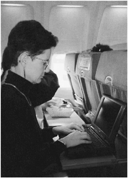
Once airborne, the businesswoman opens her laptop computer and reviews the presentation that she plans to make on her arrival. The computer 's monitor uses one of the new LIQUID CRYSTAL DISPLAY MATERIALS. Like almost every other technology in this story, the computer also depends on MAGNETIC MATERIALS.

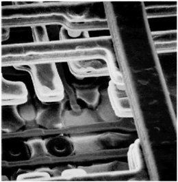
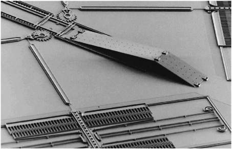
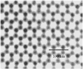
SUPERALLOYS

Superalloys are special combinations of metals that maintain high strength during prolonged exposure to elevated temperatures. This capability is essential for applications such as the turbine blades in a jet engine. Superalloys consist mostly of nickel, with smaller amounts of aluminum,titanium, chromium,and up to ten other elements. The idea behind the design of these alloys is the creation of stable, hard, small precipitates like Ni3Al or Ni3Ti in the nickel matrix to obstruct the motion of dislocations, the atomic-scale cause of undesirable deformation.

The performance of alloys in turbine blades is further improved by eliminating crystal boundaries in each blade; those boundaries are the prime sites for the initiation of fracture. Through the development of a detailed understanding of the solidification process, it is now possible to cast an entire turbine blade, with the very intricate shape shown in Figure 2.9 , as a single crystal.

Progress in alloy design and processing has led to a continuing increase in the allowable operating temperature of the turbine blades. The most recent improvements have resulted from the application of ceramic thermal barrier coatings to the outside of the blade. Increases in the operating temperature, together with improvements in the blade design (such as air cooling, through the passages seen in Figure 2.9 , made possible by sophisticated casting techniques) have greatly increased the efficiency of jet engines and decreased their weight for a given thrust.

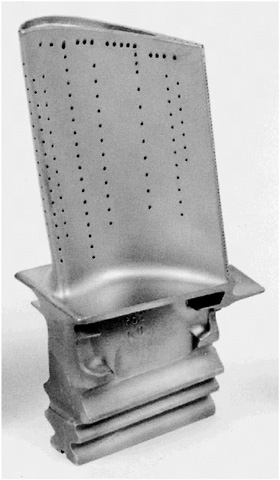
FIGURE 2.9 A turbine blade from a jet engine, cast as a superalloy single crystal. (Courtesy of GE Aircraft Engines.)

Suggested Citation:"2 Technology in Daily Life." National Research Council. 1997. The Physics of Materials: How Science Improves Our Lives. Washington, DC: The National Academies Press. doi: 10.17226/9090.
×

LIQUID CRYSTAL DISPLAY MATERIALS

Flat panel displays, such as the liquid crystal display in the laptop computer in our story, will soon be ubiquitous in both the home and the workplace, as the cost of these high-tech products is driven down by the volume market for consumers. Low-power, lighter-weight, thinner displays are already displacing the commonplace cathode-ray tube (CRT) for desktop and especially for portable applications. The portability and compactness of these displays have initiated and driven new applications and markets, such as notebook and palmtop computers, personal digital assistants, large viewing screen video cameras, miniature televisions, and individual televisions for each airline seat. Insatiable demand for lower-cost flat panel displays has created a burgeoning growth of the market from tens of millions of dollars in 1980 to about $11 billion today and to a projected $22 billion by 2001.

FIGURE 2.10 A high-resolution, active-matrix liquid crystal flat-panel display. (Courtesy of dpiX, Incorporated.)

Liquid crystals are materials in which the molecules show a preference for alignment with their neighboring molecules even though they can be in a liquid state having no long-range translational order. The molecules in these liquid crystalline phases are easy to orient by the application of an electric field and so can be made to act as a switch for light if they are placed between crossed polarizers and electrodes. Fundamental research on the physics and phase transitions of liquid crystals began in the 1920s, but it was not until the early 1970s that the first liquid crystal displays were developed. Flat-panel liquid crystal displays have only been manufactured in great volume in the last decade. Active-matrix liquid crystal displays used for the highest performance laptops today have high resolution and brightness as well as full color at high speed due to the separate electrical switching elements for each of about 1 million separate picture elements or pixels in the display. Extensive research being carried out today will eventually allow high-performance flexible displays on plastic substrates, with higher resolution and at lower manufacturing cost, which will in turn drive new technology, markets, and applications.

MAGNETIC MATERIALS

From the Ancient Mariner's compass to the automobile starter motor, from refrigerator magnets to the snapshots stored magnetically in the latest digital camera, magnetic materials have grown steadily in their importance and variety of applications. Materials display a host of fascinating magnetic properties, all of scientific interest and many of them useful in technological applications. The accelerating interplay of the science and applications of magnetism is well illustrated by the phenomenon of magnetoresistance, in which a sample exhibits a change in its ability to conduct electricity upon application of a magnetic field.

Beginning in the early 1980s, a decade of work at IBM perfected the use of magnetoresistance in a product with major commercial importance. This application, in the data sensor of the recording head within a hard disk drive, employs a single magnetic film about 200 atoms thick. The film changes resistance as it passes near a small magnetized region of a magnetic disk. Such recording heads are a growing segment of today's $30 billion hard disk drive industry. The time from Lord Kelvin's discovery of magnetoresistance in 1856 to its realization in this commercial product was 135 years.

Another class of magnetic materials, permanent magnets, are essential in a wide variety of electric motors and generators. Research and development leading to stronger magnets has resulted in a steady decrease in the cost, size, and weight of motors in such diverse devices as automobile starters, cordless shavers, hand-held drills, household appliances, toys, and disk drives (again) in laptop computers. The latest of the permanent magnet development spurts, in the late 1980s, illustrates the unpredictable effects of the interplay between politics, economics, research, and development. Samarium cobalt was the magnetic material of choice until the price of the starting materials became prohibitive due to political unrest in Zaire. Intense exploratory research discovered a superior replacement material, neodymium iron boron. The newly introduced magnets are expected to have an annual market of $4 billion within 10 years.

FIGURE 2.11 A hard disk drive assembly with a magnetoresistive sensor for reading the stored data. (Courtesy of IBM Research.)

Suggested Citation:"2 Technology in Daily Life." National Research Council. 1997. The Physics of Materials: How Science Improves Our Lives. Washington, DC: The National Academies Press. doi: 10.17226/9090.
×

The computer that analyzed the data from the MRI and CAT scans, and the computers that were involved in essentially every aspect of the airplane trip—making the reservations, assuring security at the airport, determining the flight path, and so on—are based on SILICON TECHNOLOGY.

Well into her flight and resting briefly before her important meeting, the woman relaxes in her seat and reflects on just how much of what she has taken for granted in the past several hours would have been unthinkable only a few years ago: modern cars and airplanes, telecommunications, modern medicine, the power and portability of computers. Our lives have been changed by CMMP research—and for the better.

She wonders what equally remarkable changes will take place during her son's lifetime. No one really knows, of course, but perhaps one hint can be found in new advances like INTEGRATED MICROSYSTEMS. Other ideas will arise from the scientific challenges discussed in Part 3.

Suggested Citation:"2 Technology in Daily Life." National Research Council. 1997. The Physics of Materials: How Science Improves Our Lives. Washington, DC: The National Academies Press. doi: 10.17226/9090.
×

SILICON TECHNOLOGY

Microelectronics based on silicon and its oxides underlies all of today's high-technology industries, from computers to communications to biotechnology. Microelectronics has also become common in our day-to-day lives, in applications ranging from automobiles and banking to control of household appliances.

Although silicon and germanium were used in radar detectors in the early 1940s, very little was known about the physics and materials science of these semiconductors. Scientists at Bell Laboratories soon recognized that a deeper understanding of these materials was necessary for rapid application to communications. Materials research in the mid-1940s ultimately enabled the invention of the transistor in 1947. Extensive, long-term research, along with the unexpected discovery in 1959 that silicon dioxide can passivate (protect) the surface of silicon, led to the invention of metal-oxide-silicon (MOS) transistors. The MOS transistor, combined with the increased understanding of the physics and materials science of semiconductor materials and devices that resulted from almost twenty years of intensive research and development, ultimately led to the invention of the integrated circuit.

FIGURE 2.12 Intricate layers of aluminum and tungsten wiring on an integrated circuit memory chip are revealed by etching away the interlayer dielectrics and then imaging the chip with a scanning electron microscope. The width of this image is about 10 microns (0.001 cm). A chip can contain as many as 50 million connections like those shown here in an area 1 cm on a side. (Courtesy of Lucent Technologies Bell Laboratories.)

Perhaps no other device has had as large an impact on day-to-day life as the silicon-based integrated circuit (IC). Although the IC was based on many years of condensed-matter and materials research at large industrial laboratories, the acceleration of its development and use was driven by government needs. Enabled by stable, long-term research stretching over almost two decades and stimulated by government funding, the discovery of the IC spawned the modern microelectronics industry, which is now a global enterprise. In 1995, IC sales exceeded $150 billion and supported an electronics industry with sales approaching $1 trillion. Without transistors and ICs, none of this would be possible.

INTEGRATED MICROSYSTEMS

The microelectronics industry has grown explosively over the last forty years. Such phenomenal growth has not been experienced in any other field in history. A key element behind the success of microelectronics has been integration. Integration of electronic functions on ever greater length scales leads to the low cost of production and assembly and high reliability. Miniaturization allowed for integration and simultaneously resulted in increased performance.

In the early 1980s researchers unveiled the first micromachined motor, demonstrating that the tools, facilities, and infrastructure developed to fabricate microelectronic circuits could also be used to build miniature mechanical systems. Though many research problems must be surmounted before microsystems can become as ubiquitous as the integrated circuit, this demonstration raised the hope that complex microsystems that integrate physical and chemical sensing and mechanical response with control and communications electronics can be mass produced at low cost. High-performance microsystems at lower prices would create markets for many products. In transportation, they could be used for position sensing, collision avoidance, navigation, and reliable airbag deployment. Environmental monitoring could be performed in hostile environments with inexpensive, disposable detectors. Microsystems could also be used in areas as diverse as biomedical applications and consumer products. They will probably have a profound effect on our lives and the lives of our children.

FIGURE 2.13 A prototype micromechanical mirror for use in optical communications systems. Either side of the flat hinged structure in the middle can be used as the mirror. The gears at the upper left are just just 50 microns in diameter. (Courtesy of Sandia National Laboratories.)

Suggested Citation:"2 Technology in Daily Life." National Research Council. 1997. The Physics of Materials: How Science Improves Our Lives. Washington, DC: The National Academies Press. doi: 10.17226/9090.
×
Page 4
Suggested Citation:"2 Technology in Daily Life." National Research Council. 1997. The Physics of Materials: How Science Improves Our Lives. Washington, DC: The National Academies Press. doi: 10.17226/9090.
×
Page 5
Suggested Citation:"2 Technology in Daily Life." National Research Council. 1997. The Physics of Materials: How Science Improves Our Lives. Washington, DC: The National Academies Press. doi: 10.17226/9090.
×
Page 6
Suggested Citation:"2 Technology in Daily Life." National Research Council. 1997. The Physics of Materials: How Science Improves Our Lives. Washington, DC: The National Academies Press. doi: 10.17226/9090.
×
Page 7
Suggested Citation:"2 Technology in Daily Life." National Research Council. 1997. The Physics of Materials: How Science Improves Our Lives. Washington, DC: The National Academies Press. doi: 10.17226/9090.
×
Page 8
Suggested Citation:"2 Technology in Daily Life." National Research Council. 1997. The Physics of Materials: How Science Improves Our Lives. Washington, DC: The National Academies Press. doi: 10.17226/9090.
×
Page 9
Suggested Citation:"2 Technology in Daily Life." National Research Council. 1997. The Physics of Materials: How Science Improves Our Lives. Washington, DC: The National Academies Press. doi: 10.17226/9090.
×
Page 10
Suggested Citation:"2 Technology in Daily Life." National Research Council. 1997. The Physics of Materials: How Science Improves Our Lives. Washington, DC: The National Academies Press. doi: 10.17226/9090.
×
Page 11
Suggested Citation:"2 Technology in Daily Life." National Research Council. 1997. The Physics of Materials: How Science Improves Our Lives. Washington, DC: The National Academies Press. doi: 10.17226/9090.
×
Page 12
Suggested Citation:"2 Technology in Daily Life." National Research Council. 1997. The Physics of Materials: How Science Improves Our Lives. Washington, DC: The National Academies Press. doi: 10.17226/9090.
×
Page 13
Next: 3 The Research Endeavor »
The Physics of Materials: How Science Improves Our Lives Get This Book
×
 The Physics of Materials: How Science Improves Our Lives
MyNAP members save 10% online.
Login or Register to save!
Download Free PDF

READ FREE ONLINE

  1. ×

    Welcome to OpenBook!

    You're looking at OpenBook, NAP.edu's online reading room since 1999. Based on feedback from you, our users, we've made some improvements that make it easier than ever to read thousands of publications on our website.

    Do you want to take a quick tour of the OpenBook's features?

    No Thanks Take a Tour »
  2. ×

    Show this book's table of contents, where you can jump to any chapter by name.

    « Back Next »
  3. ×

    ...or use these buttons to go back to the previous chapter or skip to the next one.

    « Back Next »
  4. ×

    Jump up to the previous page or down to the next one. Also, you can type in a page number and press Enter to go directly to that page in the book.

    « Back Next »
  5. ×

    Switch between the Original Pages, where you can read the report as it appeared in print, and Text Pages for the web version, where you can highlight and search the text.

    « Back Next »
  6. ×

    To search the entire text of this book, type in your search term here and press Enter.

    « Back Next »
  7. ×

    Share a link to this book page on your preferred social network or via email.

    « Back Next »
  8. ×

    View our suggested citation for this chapter.

    « Back Next »
  9. ×

    Ready to take your reading offline? Click here to buy this book in print or download it as a free PDF, if available.

    « Back Next »
Stay Connected!