
Panel II
Current Japanese Partnerships: Selete and ASET
INTRODUCTION
Toshiaki Masuhara
Hitachi
Dr. Masuhara, who organized the session on Japanese partnerships, offered a brief introduction of the four distinguished speakers who traveled from Japan to attend this workshop. He said they would speak on the following four topics: Selete (Semiconductor Leading Edge Technologies, Inc.); ASET, a consortium between government and industry; an overview of the Japanese consortia for semiconductor R&D; and Japan’s research centers for silicon technology.
He first introduced Dr. Morino, executive vice-president and chief operating officer of Selete.
THE SELETE PROGRAM
Akihiko Morino
Semiconductor Leading Edge Technologies, Inc. (Selete)
Dr. Morino began by describing Selete as a joint venture company that does R&D on behalf of the semiconductor industry. The company was established in 1996, and its shareholders include Fujitsu, Hitachi, Matsushita, Mitsubishi, NEC, Oki, Rohm, Sanyo, Sharp, Sony, and Toshiba—the major electronics companies of Japan. Its clients include all of those shareholders plus the Korean firm Samsung, and Seiko Epson. It is capitalized at roughly U.S. $42 million, has a budget of about U.S. $100 million, and is located in Totsuka, Yokohama.
The Mission of Selete
The mission of Selete is to develop process technologies and semiconductor devices that can be produced at reasonable cost. It also promotes the development of production equipment and materials for device manufacturers.
He placed its formation in the context of other industry consortia in the semiconductor industry. The first was the “very famous” Association of VLSI Technologies Development, which functioned from 1976 to 1980. During the 1980s there was virtually no collaboration among industries, but in the 1990s activity accelerated rapidly. In 1994 SIRIJ (Semiconductor Industry Research Institute of Japan), the think tank for the semiconductor industry in Japan, was formed. In 1995 came STARC, a university-industry collaboration. In 1996 came the formation of Selete, ASET, and VDEC, or Chip Implementation of Systems Designed by Universities. They were followed quickly in 1998 by VSAC, Support of System LSI Development, and STRJ, and the Semiconductor Technology Roadmap Committee.
A Program with Three Objectives
Based on the proposals of SIRIJ, Selete was established as a program with three objectives: The first was to promote and evaluate technologies, especially manufacturing equipment and materials for 300-mm wafers. The second was to develop advanced technologies, such as lithography and mask programs and technology CAD. The third was to carry out special projects, such as reduction of Per Fluoro Compounds (PFC) emissions. Regarding the first objective, in Phase 1, from 1996 to 2000, it worked on up to 180-nm technology and in Phase 2, from 2000 to 2001, up to 130-nm technology materials. Metrics were set up to be as specific as possible. The first year was devoted to process performance, the second year to productivity performance, and the third year to service performance. Selete also worked with suppliers to encourage development from the supplier side.
Collaboration
Collaboration with Tool Suppliers
Selete worked in collaboration with the tool suppliers. In this work Selete’s first responsibility was to set up tool performance metrics, including performance metrics for process, reliability, and productivity. Its second responsibility was tool evaluation through a module process and data feedback. Its third responsibility was to supply processed wafers to tool suppliers.
Next, Dr. Morino discussed fabrication productivity improvement. Phase 1 included equipment or automatic material handling systems, communications, and control between the various production tools. In the first phase, 193-nm li-
thography and mask technology were developed along with electron-beam direct-writing technology. These technologies were then transferred from ASET to Selete, whose task it was to continue the first phase of development
The second phase entails Selete’s focus on the execution of device process development, corresponding to the Asuka project. The four major R&D objectives associated with this phase are the development of:
-
157-nm lithography, mask, and electron-beam projection lithography;
-
a transistor that employs a high-k dielectric as a gate insulator;
-
a multilayer interconnect that employs a low-k dielectric as an inter-layer insulator; and
-
a test fabrication line, consisting of 300-mm wafer equipment, as a platform to carry out the above three objectives.
At present, said Dr. Morino, electron-beam projection lithography (EPL) is one of the most promising techniques. Selete was focusing on 157-nm and EPL as future lithography options.
He then described Selete’s role in lithography development as related to four fields: exposure tool suppliers, mask suppliers, mask defect inspection and repair tool suppliers, and resist suppliers. For Selete a critical issue is to promote R&D on the supplier side at the time required by the need for a device of a certain size; the company is now focusing on this subject.
Collaborating with Academia
As for technology CAD development, Selete has developed a framework to collaborate with academia and focus on three-dimensional process simulation and three-dimensional device simulation—a “very important field, we think.” Simulation is very important in encouraging tool model development and in delivering the framework for easy implementation of each concept as a model.
International Collaboration
He turned to international collaboration between International SEMATECH and Selete. One main objective is the evaluation of equipment for 300-mm wafers. The partnership is trying to develop unified equipment performance metrics and to assist joint evaluation and data exchange. It has published a second edition of the “Unified Equipment Performance Metrics for 130-nm Technology.” The partnership is also developing a unified interface for equipment or AMHS and CIM communication. The results of this work will be open to the public. The third field is to develop mask technologies, beginning with development of unified specifications. It also works on repair technology for mask defects and on mask handling for 157-nm lithography.
Following on what Dr. Morino described as “the fast pace of the restart of the industry-university collaboration,” in Phase 2 Selete will focus on Project Asuka,20 scheduled to run from 2001 through 2005 with the goal of developing system-on-a-chip technology in the 100- to 70-nm range. The original name of the project was ASCA, an abbreviation for Advanced System-on-a-Chip through Collaborative Achievement. The project’s name was later changed to Asuka.
The Asuka project includes a design technology field and a device-process technology field. The device-process field will involve three technology fields on a five-year development schedule. Selete will carry out device process technology, while design technology will be carried out by the STARC. He concluded by saying that Project ASCA has been undertaken in collaboration with equipment and materials suppliers, ASET, research institutes, universities, and overseas consortia. The project is also open to other potential members.
DISCUSSION
A questioner asked how the budget of Selete compares with that of SEMATECH, which in the early years consisted of $100 million of federal money matched by $100 million of private funds. Dr. Morino said that Selete’s budget is roughly U.S. $100 million, all provided by the 11 industry shareholders plus Samsung and Seiko Epson, the two client firms. It receives no government money.
THE ROLE OF ASET
Hideo Setoya
Association of Super-Advanced Electronics Technologies (ASET)
Mr. Setoya, the executive director of ASET, remarked that some people have wondered what could come after “super-advanced.” He responded by saying that “super” is enough for a few decades, and then they may decide to call it “ultra- or hyper-advanced.”
The Characteristics of ASET
He began by describing the characteristics of ASET, as follows:
-
A research body of national R&D programs for semiconductors, hard disks, and liquid-crystal displays;
-
A consortium of the electronics device industry that also includes equipment and materials suppliers (of 41 members, 6 are non-Japanese companies or subsidiaries);
-
A mission to perform research between the basic and applied levels;
-
Research performed under contract to NEDO (New Energy and Industry Technology Development Organization) by the staffs of the member companies;
-
Projects 100 percent financed by the national government with all results open to the public; and
-
International collaboration.
Initiating New Projects
He then described the process for initiating new R&D projects, which involves trade associations, MITI (Ministry of International Trade and Industry), AIST (the Agency for Industry, Science, and Technology), and numerous research committees with members from industry, academia, and government. In the case of semiconductor research, proposals are initiated by industry through an industrial think tank organized in 1994. When a proposal is adopted by MITI, it is passed to the federal budget for funding. If the topic is purely application, it is funded by private ventures. For semiconductor research the proposal goes to Selete for the pre-commercial phase of the research. MITI requests the following year’s budget through the minister of finance, who prepares the official budget draft for the cabinet. After the budget proposal is approved by the Diet, MITI assigns research funds through NEDO, which publicly announces the program for the new project.
ASET: A Research Consortium
ASET has the legal status of “research consortium,” which was established under a special law. In such a consortium all members share equal partnership, and participation is open, subject to approval by two-thirds of the member companies. Research consortia are usually organized around specific research subjects, but ASET is unusual in having three major areas of research. And while most research consortia can get tax incentives for research equipment, this is not the case with ASET, because the equipment it uses is owned by NEDO. Finally, a research consortium usually terminates after the authorized research period has expired, but ASET, which was supposed to end in 2000, was extended for three more years.
The difference between ASET and Selete is that ASET is funded by the government whereas Selete is 100 percent funded by industry, although in both cases development is done by assignees from individual member companies. In the case of the universities, most funds come from the government. However, industries are encouraged to make joint agreements or fund research in universities. In the case of government-owned laboratories, there are few industry contri-
butions, but the national laboratories are scheduled to change rather drastically, so it will have more industry funding.
Performing Pre-competitive Research
Within the spectrum of the semiconductor-related research activities sponsored by MITI, ASET’s activities fall in the mid-range between basic and pre-competitive. Universities perform most of the basic research, while Selete performs pre-competitive research and companies perform competitive research. Current ASET projects include semiconductors (by far the largest), semiconductor equipment, PFC alternative technology, and electronic system integration. (See Figure 5).
The ASET research schedule for semiconductor-related projects features a variety of lithography programs, including argon fluoride lithography (ArF), proximity X-ray lithography (PXL), extreme ultra-violet lithography (EUV), and electron-beam direct writing and mask writing. All the programs started at the end of 1995 and were scheduled to finish by the end of 2000. However, several new programs were begun that have changed the schedule. These include development of semiconductor equipment, development of F2 lasers, PFC (PerFluoro compounds) alternative technology, and electronic system integration development programs.
All Research Originates from Contracts
At ASET all research is contract research with NEDO. Actual research is performed at two types of facilities. The first is the research centers, operated by ASET, where participating members assign researchers to work. The second is a system of satellite laboratories, where one member company performs the project with its own facility and staff. In the case of research centers, which are newly built or rented facilities, ASET has to provide all the equipment. In most cases 100 percent of the research funds come from NEDO, but in fact these funds do not cover the cost of the researchers. In some cases the money does not meet the operation costs of the centers. ASET then raises money from member companies. A few projects include joint research between universities and national laboratories.
ASET’s head office is in Tokyo; its five research centers are distributed around the country, along with some branch offices, satellite labs, and university partners.
All ASET research results must be open to the public. Report seminars are held each year and these are open to the public. The materials are distributed in Japanese as well as in English and technical papers are submitted to the academic societies. In the course of ASET studies, more than 10 researchers from the member companies have received doctorate degrees through ASET research.
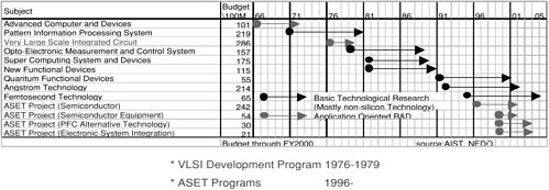
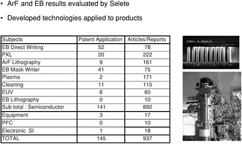
FIGURE 6 Selete achievements (as of March 2000).
The treatment of patent and other industrial property rights is in the process of change. Before September 2000 old patents and other property rights were shared by NEDO and ASET. ASET’s share was transferred to the company that was the actual inventor. After five years, outside companies could use the patent with the approval of NEDO and the other owner. As of October 2000, however, the contractor could claim 100 percent ownership of the patents. This change was meant to encourage the contractor to apply for more patents through the national programs.
Mr. Setoya showed a list of the achievements of ASET, including patent applications, articles, and reports. (See Figure 6.) The research results of the ArF and electron-beam projects have been evaluated at Selete. In addition, some of the developed technologies have already been applied to commercial products. The total number of patent applications to the end of March 2000 was 145, and the, total number of articles and reports was 937.
International Cooperation
Finally, he showed the results of international cooperation in ASET. There were 41 members, including TI Japan, IBM Japan, Merck Japan and Merck KGaA, Samsung, and Intel. The first three were the original members of ASET, and Merck KGaA joined ASET soon after. Intel and Samsung joined the EUV lithography research, and Samsung also participated in the PFC alternative technology research.
ASET sponsors the International Forum on Semiconductor Technology along with ISMT, IMEC, and other research consortia. They have held three forums: two in Kyoto and one in Monterey, California. In 2001 they will hold the Fourth International Forum on Semiconductor Technology in Antwerp, Belgium. ASET has also hosted many technical meetings, including meetings on 193 nm, Hi-CP, XEL, plasma, 157 nm, and EUV. ASET has also been responsible for direct exchange of information with other companies and research consortia.
Mr. Setoya concluded by saying the future of ASET is not clear, but it plans at least to extend the EUV and, possibly, the EB (electron-beam) program for a second phase. He expressed the hope for additional international cooperation for development of EUV technology.
ASET is to start two new programs in 2001. They are the MIRAI Project to develop next-generation basic technology for semiconductor process and material, including high-k and low-k research, and the HALCA Project to develop the highly agile minifab concept. MIRAI is a joint program between the newly reorganized national laboratory, Advanced Semiconductor Research Center (ASRC) of the National Institute of Advanced Industrial Science and Technology (AIST), and ASET.
DISCUSSION
Technology Transfer
Phillip Webber of the Congressional Budget Office asked if there were technology transfer mechanisms for ASET other than international collaboration. He asked also how the technology that was developed in satellite labs would make its way into the public domain or to other members of ASET. Mr. Setoya answered that the transfer of technology was the responsibility of the patent holder if the patent was included in the technical results. The overall technological papers themselves are public, but the patent holder would decide if third parties could use the patent. In the field of semiconductors, he pointed out, most companies had cross-licensing agreements, and so patents were not a big barrier.
To a question about the budget he answered that in the case of ASET almost $370 million had been paid in by the government in the past five years. The total budget, including development of magnetic storage and LCD programs, came to $500 million.
Mingae Song, a graduate student in the economics program at Harvard, asked about the different market structures of DRAMs and microprocessor chips. For DRAMs the market is globally very competitive but for microprocessor chips Intel has about 80 percent of the whole market share. The question was how much weight ASET puts on microprocessor chips in R&D. Dr. Setoya said that ASET does not do research on specific products. It supports fundamental technology for semiconductors overall, such as lithography and basic materials.
JAPANESE CONSORTIA FOR SEMICONDUCTOR R&D
Yoichi Unno
Semiconductor Industry Research Institute of Japan (SIRIJ)
Dr. Unno said that much had already been explained about Japanese consortia for semiconductor R&D but that he would add his own perspective. SIRIJ was founded in 1994 as a think tank by 10 Japanese semiconductor companies to promote joint R&D of silicon technology. The objectives of SIRIJ were to plan and promote the development of next-generation semiconductor technologies, to study the future of the semiconductor industry, and to implement projects for international cooperation within the semiconductor industry. Corporate members include the leading members of the semiconductor industry from Fujitsu to Toshiba.
A Spirit of Cooperation
Activities of SIRIJ were helped by a spirit of cooperation between academia and industry in 1995, when the Japanese were lagging behind in the semiconductor industry. (See Figure 7.) SIRIJ planned and proposed joint research systems with Japanese universities and industry, and STARC (Semiconductor Technology Academic Research Center) was established in 1995. In 1996, he said, the Japanese semiconductor industry was still in decline. Many semiconductor in
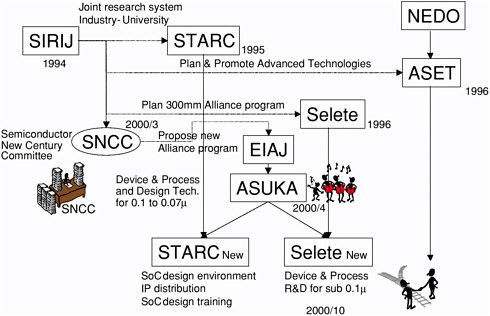
FIGURE 7 Historical flow of Japanese consortia.
dustries could not afford the development expense of 300-mm equipment, so SIRIJ planned a new alliance to develop leading-edge semiconductor technologies. The result was Selete, founded in 1996 by 10 companies. Also in 1996 SIRIJ planned and promoted ASET, the Association for Super-Advanced Electronic Technologies.
Other activities were educational. The universities were already educating students, but there was a need to educate more and to provide continuing education for people in small design companies and venture businesses. Therefore, in 1998 SIRIJ started an organization called VSAC (Venture System LSI Assist Center) to promote LSI design by small design companies and to provide support.
In addition, in 1998 SEMATECH and the SIA asked all major semiconductor firms to help produce an international roadmap for semiconductors. SIRIJ planned and organized a new committee called STRJ, the Semiconductor Technology Roadmap Committee of Japan, in 1999.
Revitalizing the Industry
The final step for SIRIJ was to organize a team to study the needs of the industry for the new century with the objective of revitalizing the Japanese semiconductor industry. The corporation proposed a new strategic plan for global competitiveness called “The Revitalization of the Japanese Semiconductor Industry,” published in April 2000. He summarized the recent history of Japanese consortia with a flow chart from 1994 to 2000.
Evaluations
Evaluations by Managers
After reviewing the Selete program (described earlier), he discussed a SIRIJ program designed to evaluate the production of 300-mm equipment. The evaluation was done by managers of the 10 client companies, who assigned grades of blue (good), green (acceptable), or white (poor). For LP/AP-CVD (low-pressure/ atmospheric pressure-chemical vapor deposition), 90 percent of the managers rated the performance acceptable. For ox-diffusion-RTP (rapid thermal processing), 80 percent judged it acceptable. However, for lithography and etching, only 60 percent of managers judged it acceptable. AMHS (automated material handling systems) was given a grade of acceptable by 60 percent of the managers, and for cleaning—CMP (chemical mechanical polishing or planarization)—only 50 percent assigned a grade of acceptable. He said that in his personal opinion, much more money is required to develop advanced etching process technologies. For cleaning, he said, more progress is needed. As for AMHS, he noted that he did not altogether understand the problem but thought that many companies had different policies in this regard.
Evaluation by Engineers
Next, he reviewed SIRIJ’s advanced technology program evaluation, carried out by engineers of the 10 client companies. Research and development activities had the highest scores, with almost 70 percent rated acceptable. Argon fluoride resist needed more support, he said, and optical mask was a very challenging technology, but he said that the industry seemed to be finding its way. EB (electron-beam) direct writing disappointed many people, with only 8 percent acceptable, and TCAD (technology Computer-Aided Design) also “left our head down,” with only 17 percent acceptable. Finally, he mentioned a comprehensive evaluation by the managers in 1999 of timing, investment efficiency, and development results. Almost 80 percent of the managers gave a grade of acceptable, which Dr. Unno said was “not bad, but maybe an easy path.”
Turning to ASET, he mentioned the interim evaluation of laboratories performed in 2000 by both technical committee members and ASET department managers. Illustrating the results with humorous cartoon figures, he summarized that EUVL and environmental technologies did well, PXL did fairly well, plasma needed help, and cleaning needed “a lot of help.”
UNIVERSITY RESEARCH CENTERS FOR SILICON TECHNOLOGY
Masataka Hirose
Hiroshima University
Government-sponsored Research
Dr. Hirose, who was director of the Research Center for Nanodevices and Systems at Hiroshima University, said that he would offer an overview of Japanese university research centers for silicon technology. He noted that he would focus on three centers and mention some recent research activities. The three research centers are all sponsored by Monbusho: Ministry of Education, Science, and Culture.
The first center is VDEC, the VLSI Design and Education Center, established in May 1996 at the University of Tokyo. VDEC services include:
-
Distributing the latest technology information on VLSI design and education;
-
Providing media, licenses, and training courses for CAD (Computer-Aided Design) tools; and
-
Supporting VLSI chip fabrications and measurement for academic use.
By 1999 VDEC had 120 institutional users, including national and private universities, and a total of about 350 professors making use of VDEC activity. By
1999 nearly 300 chips were fabricated by client companies NEC, Motorola, Rohm, and Hitachi.
Techniques for Mobile Networks
The second center is the New Industry Creation Hatchery (“incubation”) Center located at the Department of Electrical Engineering of Tohoku University. A major program, called Monbusho Scientific Research on Priority Areas, aims to produce new image-processing techniques for mobile network applications, including applications for the motion picture industry. From 1996 to 1999 the center’s program featured “ultimate integration of intelligence on silicon electric systems.” This was a joint research project involving about 20 university groups focusing on applications-oriented research. From 2000 to 2003 the center will focus on “mixed integrated systems for real-time intelligence processing,” again involving about 20 university research groups.
Another part of the work at Tohoku University consists of the MITI R&D Program, supported by NEDO. The major purpose of this program is to develop strategic manufacturing tools. The major projects include the following:
-
A microwave-excited plasma tool using a radial-line slot antenna (this tool features a high-density, uniform, and low-electron-temperature plasma and also a high-accuracy plasma process without metal contamination or surface damage);
-
A balanced electron drift magnetron plasma-etching tool;
-
A multi-target, long-throw balanced electron drift sputter tool; and
-
A vertical integrated cluster tool.
The third center is the Research Center for Nanodevices and Systems at Hiroshima University. Research projects include advanced metrology for high-k gate dielectrics, modeling of gate tunnel leakage current, 30-nm gate-length MOSFETs,21 and Cu drift in low-k dielectrics.
To illustrate one focus of the work at this center he showed a graph of a direct tunnel regime and a second graph of a 30-nm gate length MOSFET, with drain voltage plotted against drain current. Finally, he showed a series of energy band profiles of MIS structures with high-k gate dielectrics. A second emphasis at Hiroshima University is CREST, the Core Research Program on Science and Technology, supported by the Agency of Science and Technology (AST). CREST sponsors an effort to understand the self-assembling of silicon quantum dot and its application to floating gate MOSFETs.
DISCUSSION
Greg Linden of the University of California at Berkeley asked whether the research programs described were part of STARC. Dr. Hirose said they were completely separate, supported basically by the Ministry of Education and Sciences.
Concerns Over Research Support
Dr. Wessner recalled the concern of several American speakers about the level of basic research supported by the U.S. government and asked whether this was also a concern in Japan. Dr. Hirose said that the universities should indeed focus on fundamental research, but that they should also understand the practical problems of industry, so that near-term work also requires university involvement. He said that good balance between applied science and fundamental research work will be one of the important missions of the university research involvement, which is a basis for startups, new ideas for the future, device technology, and material technology.
Funding Levels at Universities
Genda Hu of Taiwan Semiconductor Manufacturing Company asked Professor Hirose about the general funding level of the three university programs. Professor Hirose said it varies year by year, but the base level is at least a few million dollars annually, provided by the government for learning centers. Additionally, depending upon the application, programs would receive more than $5 million per year to support new equipment or meet replacement needs.
Jeffrey Gren of the U.S. Department of Commerce asked if the current Japanese focus on DRAMs might change in the future as a result of the activities outlined today. Professor Hirose answered “maybe,” and noted that the question is very delicate. He said that in Japan many companies cooperate in developing next-generation technologies, such as Hitachi and Toshiba, because they want to reduce development costs. That, he said, is a new fashion in Japan.
Urging Consortia to Collaborate
Mr. Gren then asked why there were multiple R&D consortia in Japan, in addition to International SEMATECH, and whether they might be combined in a single international framework. Professor Hirose agreed that this is desirable and said that there have been several examples of international collaboration between consortia. He said that a higher level of international collaboration is needed to both conquer technical barriers and reduce costs. “The issue,” he said, “is how to
collaborate effectively on specific items.” He called for more experiments in collaboration, some trial-and-error, to learn the best ways of doing it.
William Joyner of the Semiconductor Research Corporation said that he was under the impression that STARC in its previous incarnation would support university research at several Japanese universities. Now it has moved primarily toward training designers for system-on-a-chip design. He asked whether another organization had stepped in to continue funding the projects that used to be funded by STARC. Toyoki Takemoto of STARC said that the organization continues to be funded by industry to do collaborative research with universities but that more assistance was needed for education, especially curriculum reform.
An Expertise Gap
Dr. Moore recalled the need for more technical graduates in the United States and asked whether such a huge supply-and-demand gap existed in Japan as well. Dr. Masuhara said that the total number of students graduating from electrical engineering programs had not fallen in Japan, but he said that several years ago a study of expertise needed by industry revealed a large gap. In the field of designing VLSI chips company demand was four times larger than the number of students, a ratio that has not improved and is probably increasing. He said that was the reason Dr. Takemoto had mentioned the need for improved university education, particularly for the design of the silicon chip system.


