
Issues Associated with the Volume Manufacturing of Vertical-Cavity Surface-Emitting Lasers
THOMAS M. BRENNAN AND H. Q. HOU
EMCORE Photovoltaics
Albuquerque, New Mexico
ABSTRACT
Vertical-cavity surface-emitting lasers (VCSELs) have been grown by metal-organic chemical vapor deposition. Excellent uniformity of Fabry-Perot cavity wavelength for VCSEL materials of ±0.2 percent across a 3" diameter wafer was achieved. This results in excellent uniformity of the lasing wavelength and threshold current of VCSEL devices. Employing pregrowth calibrations on growth rates periodically with an in situ reflectometer, we obtained a run-to-run wavelength reproducibility for 770- and 850-nm VCSELs of ±0.3 percent over the course of more than a hundred runs. These developments have brought VCSEL devices out of the laboratory and into the commercial arena, where they are now available for many advanced technical applications, such as optical communications, biomedical applications, consumer electronics, and optical computing. The ability to manufacture very exquisite light sources, such as the VCSEL, theoretically for the cost of a light-emitting diode, provides for the first time the opportunity to economically process multitudes of information with light.
INTRODUCTION
Vertical-cavity surface-emitting lasers (VCSELs) are promising for a variety of applications such as optical interconnects, optical communications, optical recording, and remote sensing (see, for example, Lee, 1995). Growth of VCSEL materials requires a wide range of composition and doping-level variation. Metalorganic chemical vapor deposition (MOCVD) technology is increasingly recognized as a superior epitaxy platform because of its high throughput, continuous compositional grading control, flexibility for materials and dopant choices,
and the ability to achieve low surface defect density (Hibbs-Brenner et al., 1996; Sun et al., 1995). However, the material uniformity across the entire wafer is often limited by the complex fluid and thermodynamics in a reactor. Another important concern lies in the run-to-run reproducibility. It is essential that thickness and composition control for a VCSEL structure be accurate to align the distributed Bragg reflector (DBR) stopband, Fabry-Perot mode, and the active-layer gain spectrum to a specific wavelength range. Slight day-to-day variation can drift the VCSEL wavelength and change the laser characteristics significantly. Recently, it was shown that good reproducibility and uniformity can be achieved from MOCVD-grown VCSELs (Hibbs-Brenner et al., 1996; Sun et al., 1995). However, the traditional geometry of the MOCVD reactor prohibits the use of in situ tools, such as pyrometric interferometry (Houng et al., 1994) and ellipsometry (Aspnes et al., 1990), which are commonly used in a molecular beam epitaxy (MBE) system for growth monitoring. The MOCVD growth conditions are usually determined in advance through an often tedious set of calibration runs. In this paper we demonstrate excellent reproducibility for VCSEL growth employing pregrowth calibrations with an in situ reflectance setup (Breiland and Killeen, 1995; Hou et al., 1996; Kawai et al., 1987) and high material uniformity by optimizing the growth conditions.
MOCVD GROWTH AND IN SITU REFLECTOMETRY
Epitaxial growth was performed in an EMCORE GS3200 MOCVD rotating disk reactor. GaAs and AlxGa1-xAs were grown at 750°C by using trimethylgallium. (TMG), trimethylaluminium (TMA), and 100 percent arsine (AsH3). Dopants for n-and p-type materials were from disilane (Si2H6) and carbon-tetrachloride (CCl4), respectively. The alkyl and doping precursors were mixed in an injection block, and were carried by high-purity H2 to the EMCORE vertical reactor through three different injection zones distributed along the radial direction on the top flow-injection flange. The AsH3 was injected through two other zones. The reactants were isolated from the stainless steel chamber wall with a high hydrogen flow along the shroud. Therefore, there is little upstream contamination or carryover to a substrate. The substrate was rotated at 1,000 rpm. The reactor pressure was 60 torr.
The normal-incidence reflectance setup consists of a 7-watt W-halogen lamp as the light source and a silicon detector with a 10 nm bandwidth interference filter at 633 nm to detect the reflectance signal. The whole assembly was mounted directly on the top miniflange window of the reactor. A virtual interface model (Breiland and Killeen, 1995) extracts the growth rate and optical constants from the absolute reflectance of only the topmost layer by referencing the starting signal to the known reflectance of the substrate before epitaxy begins. It does not require any knowledge of epitaxial materials, interface position, thickness, or composition of underlying epitaxial layers. This provides a simple,
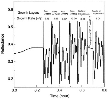
FIGURE 1 Temporal reflectance of a typical calibration run for the growth rate and etchback rate during AlGaAs growth. Within an hour, growth and etchback rates are obtained for the various growth conditions.
robust, and accurate measurement of the growth rate. Shown in Figure 1 is the temporal reflectance from a typical calibration run. The growth rates achieved by using various alkyl sources were determined from fitting the reflectance waveform with the virtual interface model. The reduction of the growth rate due to an etchback effect of AlGaAs by CCl4 with different C doping levels at different temperatures is also extracted from this single calibration run of less than an hour (Hou et al., 1996). The small deviation of the growth rate from the expected value was corrected afterwards.
MATERIAL AND DEVICE UNIFORMITY
The sample uniformity was optimized by changing the gas-flow partition for alkyl sources among the three injection zones with hydride flow partition of 80 percent: 20 percent between the inner and outer injection zones and a total reactor flow of 32.6 slm. Mirror structures of 20-period of AlGaAs/AlAs DBRs were grown under different conditions. The center wavelength of the DBR reflectivity stopband was measured for different radial positions of a 3-inch diameter
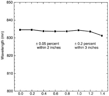
FIGURE 2 Uniformity of the center cavity wavelength for an 850-nm VCSEL sample. Excellent uniformity of ±0.05 percent is achieved in the center 2-inch area, and ±0.2 percent in the whole 3-inch area.
wafer. It was found that equal alkyl distribution among the three injection zones on the top flange did not give a uniform growth rate on the substrate. Instead, a setting of the gas-flow distribution of 7 percent:78 percent:15 percent between the inner, middle, and outer injection zones yielded the most uniform thickness. The uniformity, which is most sensitive to the partition setting, was further optimized with the AsH3 flow rate, or the V/III ratio. We found that the uniformity could be tuned slightly with AsH3 flow rates from 230 to 270 sccm, or the equivalent V/III ratio from 36 to 42.3, and the best uniformity across an entire 3'' wafer was achieved with an AsH3 flow of 248.5 sccm, or a V/III ratio of approximately 39.
Figure 2 shows the wavelength of the Fabry-Perot cavity mode for an 850-nm VCSEL structure grown with the above-optimized conditions as a function of the distance from the wafer center. The uniformity was found to be rotation symmetric except for a little disturbance near the major flat of the wafer. The wavelength for the area ~3 mm. from the wafer edge (the last data point in Figure 2) can be slightly influenced by the thickness of material coated on the suscep
tor. The wavelength variation (??) was measured to be 0.8 nm in the center 2 inches and 3.3 nm across the entire 3-inch wafer. This corresponds to a wavelength and thickness uniformity of ±0.05 percent in the center 2-inch area of the 3-inch wafer, and ±0.2 percent over the entire 3-inch wafer. Since the alkyl gases are mixed uniformly before being injected into the reactor, and the incorporation ratio of Al/Ga is fairly insensitive to a small temperature variation around 750°C, the composition variation across a wafer should be negligible. This uniformity result is believed to be among the best achievable for III/N semiconductor epitaxial technology for an entire 3-inch wafer area.
VCSELs were fabricated from the material discussed above with oxide current apertures on both sides of the cavity to provide electrical and optical confinements (Choquette et al., 1995). The structure consists of 26 periods of top and 38 periods of bottom Al0.16Ga0.84 As/Al0.92Ga0.08As DBRs. The composition was parabolically graded across the interfaces of high and low Al containing layers to reduce the series resistance. There is one period of Al0.16Ga0.84As/Al0.98 Ga0.02As DBR on each side adjacent to the cavity. The Al0.98Ga0.02 As layer can be selectively oxidized laterally in a steam ambient to form an Al-oxide current aperture since the oxidation rate of Al0.98Ga0.02As is 3.5 times higher than Al0.92Ga0.08As (Choquette et al., 1995). The lasing wavelength and threshold current of VCSEL devices with 9 × 9 µm2 oxide apertures on both sides of the cavity are plotted in Figure 3 as a function of the distance from the
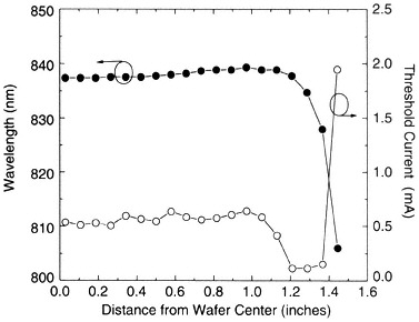
FIGURE 3 Uniformity of the lasing wavelength and threshold current of 850-nm VCSELs with 9 × 9 µm2 oxide apertures.
center of the wafer. Even with fabrication nonuniformity, the lasing wavelength uniformity is still ±0.3 percent (or variation of ~5 nm) over nearly the whole wafer. The threshold current variation is less than ±10 percent in the center 2-inch area of the 3-inch wafer. The drop of the threshold current in the outer 1-inch area is due to the laser self pulsation (Choquette et al., 1996) resulting from a high series resistance of the p-DBRs. The C-doping efficiency drops when the substrate temperature increases (Hou et al., submitted) in the outer area of the 3-inch diameter platen where the temperature is estimated to be 20~30±C higher than the center. This results in an increase of series resistance by a factor of 2 in the outer area. Therefore, slightly over-doped p-DBRs should be used to ensure a low series resistance for more uniform device performance to compensate for the inherent effect caused by temperature nonuniformity of the substrate.
RUN-TO-RUN REPRODUCIBILITY
The MOCVD growth runs are also highly reproducible when a pregrowth calibration with the in situ reflectance is performed about once every 20~30 runs. Figure 4 shows the cavity wavelengths for a number of 770- and 850-nm VCSELs plotted as a function of the run number. The cavity was not changed from run to run for the 770- and 850-nm VCSELs, but the mirror design (number of periods and doping concentration) was varied for a structure-design optimization process. Twelve 850-nm VCSELs (run number 1068 to 1073, 1114, and 1163 to 1167) and seven 770-nm VCSELs (run number 1112 to 1113 and 1115 to 1119) were grown at different times over the course of about 100 runs. Other materials and device structures were grown in between. To ensure reproducibility, a calibration run as shown in Figure 1 was carried out before a series of VCSELs were grown. Slight changes in the flow rate calibration were made accordingly. As shown in Figure 4, we obtained wavelength run-to-run reproducibility of ±0.3 percent for both 770- and 850-nm VCSELs. Since the calibration included a wide range of composition and doping levels (Hou et al., 1996), reproducible results were achieved in spite of the varying device structures.
CONCLUSION
In summary, we have demonstrated an optimized MOCVD technique for highly uniform and reproducible VCSEL growth. In situ reflectance is used to monitor the growth routinely. With a pregrowth calibration of the growth rate using a test structure periodically, ±0.3 percent run-to-run cavity wavelength reproducibility was achieved over a course of about 100 growth runs. The thickness and composition uniformity is as good as ±0.2 percent, and the lasing wavelength uniformity is as good as ±0.3 percent in most of a 3-inch wafer. This ultrahigh uniformity of the epitaxial material enables uniform VCSEL performance of a large number of VCSEL arrays. Our results show the potential of
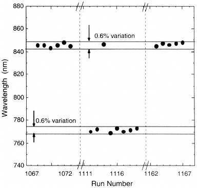
FIGURE 4 Reproducibility of the cavity wavelength of 770- and 850-nm VCSEL structures versus the growth run number. Pregrowth calibrations with the in situ reflectometer were made with Runs 1067, 1111, and 1162.
MOCVD as a very stable, reproducible, and uniform growth platform for VCSEL manufacturing.
REFERENCES
Aspnes, D. E., W. E. Quinn, and S. Gregory. 1990. Application of ellipsometry to crystal growth by organometallic molecular beam epitaxy. Applied Physics Letters 56(25):2569–2571.
Breiland, W. G., and K. P. Killeen. 1995. A virtual interface method for extracting growth rates and high temperature optical constants from thin semiconductor films using in situ normal incidence reflectance. Journal of Applied Physics 78(11):6726–6736.
Choquette, K. D., H. Q. Hou, K. L. Lear, H. C. Chui, K. M. Geib, B. E. Hammons, and A. Mar. 1996. Self-pulsing oxide-confined vertical-cavity lasers with ultralow operating current. Electronics Letters 32(5):459–460.
Choquette, K. D., K. L. Lear, R. P. Schneider Jr., K. M. Geib, J. J. Figiel, and R. Hull. 1995. Fabrication and performance of selectively oxidized vertical-cavity lasers. IEEE Photonics Technology Letters 7(11):1237–1239.
Hibbs-Brenner, M. K., R. A. Morgan, R. A. Walterson, J. A. Lehman, E. L. Kalweit, S. Bounnak, T. Marta, and R. Gieske. 1996. Performance, uniformity, and yield of 850-nm VCSEL's deposited by MOCVD. IEEE Photonics Technology Letter 8(1):7–9.
Hou, H. Q., W. G. Breiland, B. E. Hammons, and H. C. Chui. 1996. In situ growth rate measurements by normal-incidence reflectance during MOCVD growth. Electrochemical Society Proceedings 96(2):27–35.
Hou, H. Q., B. E. Hammons, and H. C. Chui. Submitted. Doping and in situ selective etching of AlGaAs with CCl4 in metalorganic vapor phase epitaxy. Applied Physics Letters.
Houng, Y. M., M. R. T. Tan, B. W. Liang, S. Y. Wang, and D. E. Mars. 1994. In situ thickness monitoring and control for highly reproducible growth of distributed Bragg reflectors. Journal of Vacuum Science & Technology 12(2):1221–1224.
Kawai, H., S. Imanaga, K. Kaneko, and N. Watanabe. 1987. Complex refractive indices of AlGaAs at high temperature measured by in situ reflectometry during growth by metalorganic chemical vapor deposition. Journal of Applied Physics 61:328–332.
Lee, T. P., ed. 1995. Current Trends in Vertical Cavity Surface Emitting Lasers. Singapore: World Scientific.
Sun, S., E. Armour, K. Zheng, and S. D. Hersee. 1995. Ultra-Uniform MOCVD Growth of GaAs/ AlGaAs for VCSELs. Pp. 123–127 in Proceedings of the 7th Biennial Workshop on Organometallic Vapor Phase Epitaxy. Fort Meyers, Fla., Apr. 2–6, 1995.
Optical Applications of Microelectromechanical Systems
MING C. WU
Electrical Engineering Department
University of California
Los Angeles, California
ABSTRACT
Microelectromechanical systems (MEMS) technology has opened up many new opportunities for optics. For the first time, reliable microactuators and three-dimensional optomechanical structures can be monolithically integrated with micro-optical elements. This new technology will impact many applications including display, scanning, and telecommunications. In this paper, we will discuss two MEMS applications: optical systems on a chip and monolithic integration of a large array of optomechanical devices.
INTRODUCTION
Integrated optical systems have been a dream of many optics researchers for decades. Though some progress has been achieved in semiconductor optoelectronics, most of the other optical systems are still made of discrete components and assembled precisely on optical breadboards. As a result, these optical systems are expensive and bulky. Recent advances in MEMS have made it possible to produce compact optomechanical structures and microactuators at low cost, using batch-processing techniques. These advances have opened up many new possibilities for optical and optoelectronic systems, including optical systems on a chip, and monolithic integration of a large number of optomechanical devices. MEMS technology provides a paradigm shift for optics from labor-intensive manual assembly to batch fabrication using integrated circuit-type microfabrication. Compared with conventional optical systems, MEMS optical systems (also called micro-optoelectromechanical systems or MOEMS) offer many advantages (Muller and Lau, 1998; Wu, 1997) by being more compact, lighter, faster, more
rugged, and more scalable. Their applications include projection and head-mounted displays, optical data storage, printing, optical scanners, switches, modulators, sensors, and optoelectronic components packaging.
This paper describes two types of applications for optical MEMS: (1) optical systems on a chip, and (2) monolithic integration of a large array of optomechanical devices. Specific examples will be given for each type of application.
OPTICAL SYSTEMS ON A CHIP
MEMS technology has made it possible, for the first time, to integrate an entire optical table onto a single silicon chip. Optical elements such as lenses, mirrors, and gratings are batch fabricated along with the XYZ stages (micropositioning stages with three independent degrees of freedom) and the microactuators. (See Figure 1 for an example of a single-chip MEMS optical system.) The discrete lenses and bulk optomechanical supports are now batch fabricated and monolithically integrated on a single chip. As a result, the size of the system can be dramatically reduced by one to two orders of magnitude.
The main challenge to implementing single-chip optical systems is the ability to make different optical components using the same fabrication process. Typical optical components for free-space optical systems include (1) optical elements such as lenses, mirrors, and refractive and diffractive optical elements; (2) three-dimensional optomechanical support, such as lens mounts; and (3) adjustable structures and actuators, such as XYZ micropositioners. In the last several years, our research group at the University of California, Los Angeles (UCLA) has been developing a MEMS optical bench technology that can simultaneously fabricate these three types of components using the same fabrication process. Our fabrication process is based on standard polysilicon surface-micromachining processes. Such processes are now available through commercial foundries (e.g., the multi-user MEMS processes, or MUMPs, offered by Cronos Microsystems). MUMPs is a three-polysilicon surface-micromachining process in which the two structural polysilicon layers can be selectively patterned and released to form free-standing structures. Details of the MUMPs process can be found at http://mems.mcnc.org/mumps.html.
One of the most commonly used optical components in free-space optical systems is XYZ stage. Building micro-XYZ stages using MEMS technology is a challenging task. The out-of-plane translation is particularly difficult since most of the surface-micromachined actuators move in the in-plane directions. We have overcome this difficulty by using a novel micro-elevator-by-self-assembly (MESA) structure (Fan and Wu, 1997). MESA consists of five polysilicon plates joined by microhinges. When the two outer plates are moved towards each other, the center plate will buckle up and rise above the substrate. By integrating MESA with the two sliding structures a full micro-XYZ stage with three independent degrees of freedom is achieved. The scanning electron
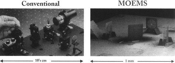
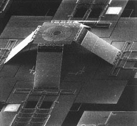
FIGURE 2 Scanning electron micrograph of a micro-Fresnel lens integrated on a micro-XYZ stage. The micro-XYZ stage has three independent degrees of freedom, with the travel distance greater than 100 µm in all three directions. SOURCE: UCLA.
micrograph of the micro-XYZ stage is shown in Figure 2. It is integrated with scratch drive actuator arrays. The scratch drive actuator is basically a stepper motor with an extremely fine step size (Akiyama et al., 1997). It consists of a polysilicon plate with a vertical bushing. Upon application of an electrical pulse, the electrostatic force will deform the polysilicon plate. The downward motion pushes the front bushing forward by a small step. Upon release of the bias, the friction at the front bushing, which is larger than at the backside of the plate, pulls the entire scratch drive actuator forward. The average step size is extremely fine, 20~30 nm, which is ideal for positioning optical elements requiring sub-0.1 µm accuracy.
Micro-optical elements can be monolithically integrated with the actuated micromechanical structures. One of the unique advantages of MEMS optical bench technology is that all three-dimensional structures are assembled after the fabrications are finished. Before the micromechanical. structures are released, the surface of wafers remains planar. Therefore, we can combine MEMS with the well established planar micro-optics technology to build three-dimensional optical components. For example, a refractive microlens is monolithically integrated with a three-dimensional lens mount by using reflow technique. A cylinder of polymer (e.g., photoresist) is patterned on the polysilicon plate. It is then heated up at a high temperature, causing the polymer cylinder to reflow. The surface tension will pull the surface into a spherical shape. This is illustrated in Figure 3. Microlenses with a wide range of f—number and aperture can be
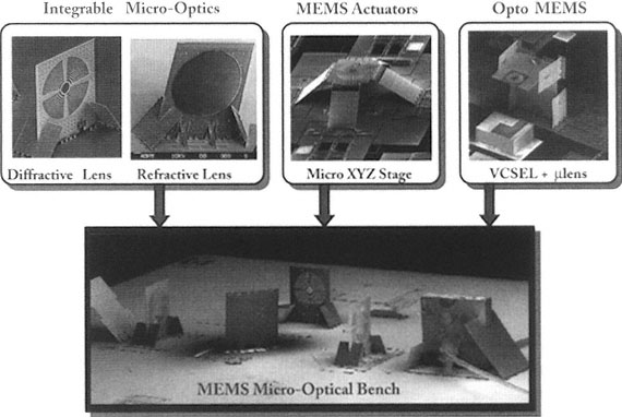
made by this technique. Diffractive optical elements can also be readily incorporated into the MEMS structures. We have also successfully used the micro-fabricated XYZ stage to position a bulk microlens with 300 micrometer diameter. Hybrid integration with active optoelectronic source and detectors are also of interest. We have successfully integrated a vertical surface-emitting laser with a suspended microlens, as shown in Figure 3.
Using the building blocks described above, we have built several optical systems on MEMS micro-optical benches. A femtosecond autocorrelator has been constructed to measure the pulse width of extremely short optical pulses (120 femtoseconds has been demonstrated experimentally). A single-chip optical disk pickup head has also been realized.
LARGE ARRAY OF OPTICAL MEMS DEVICES
Like integrated circuits, a large number of optical devices can be integrated on the same chip using MEMS technology. This is similar to the random access memory of electronic integrated circuits. The most well-known example of this type of optical MEMS device is perhaps the digital micromirror device of Texas Instruments, which consists of more than one million torsion mirrors. The digital micromirror device (DMD™) has been used in commercial projection display systems, and is particularly attractive for compact portable projection systems.
In addition to display, MEMS optical devices are very attractive for telecommunication applications, including optical switches, optical crossconnect, wavelength division add/drop multiplexers, and tunable lasers/detectors. MEMS optical switches offer many advantages over other types of switches, including low insertion loss and low crosstalk. They are transparent to the optical data and are independent of polarization, wavelength, bit rate, and modulation format. Moreover, MEMS technology allows a large number of switches to be integrated on a single substrate. This is very attractive for optical crossconnect applications. The basic building blocks of a MEMS optical crossconnect is illustrated in Figure 4.
Under Defense Advance Research Project Agency support, UCLA has been investigating manufacturable, low-cost fiber optic switches using MEMS technology. Figure 5 shows the scanning electron micrograph of our first-generation MEMS fiber optic switch (Lee et al., 1997). It consists of a moveable micromirror, four fiber guides, a mechanical restoring spring, and microactuators. Depending on the mirror position, light emitted from the input fiber is either transmitted to the opposite fiber or reflected to the orthogonal fiber. The scratch drive actuator and a restoring spring are used to move the micromirror. The restoring spring allows the switch to be used as a bypass switch for the fiber distribution data interface (FDDI) ring networks. During power failure, the spring always pulls the mirror back to the bypass state to maintain the continuity of the fiber ring network. The switch has been successfully demonstrated. Low

FIGURE 4 Schematic of MEMS optical crossconnect. SOURCE: UCLA.
insertion loss was obtained, however the switching time is on the order of 10 msec. Though this is sufficient for FDDI applications, sub-millisecond switching times and low operating voltages are desired for many other applications.
For optical crossconnect applications large mirror areas and low operating voltages are desired. There is, however, a trade-off between these two parameters. A large mirror area requires a large displacement, which translates into high operating voltages for typical electrostatic actuators. Recently, we devel
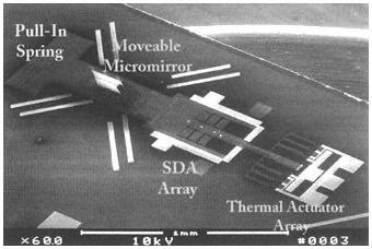
FIGURE 5 Schematic of the first-generation MEMS fiber optic switch made at UCLA. SOURCE: UCLA.
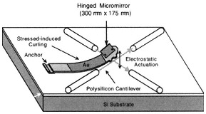
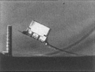
FIGURE 6 Schematic and photograph of the curled cantilever MEMS optical switches. SOURCE: UCLA.
oped a novel curled cantilever switch (Chen et al., 1999) that can overcome this trade-off. Figure 6 shows the schematic drawing and photograph of the switch. The micromirror is attached to the end of the curled cantilever beam. The actuation voltage is determined by the initial small gap, while the mirror displacement is determined by the motion of the tip. We have achieved a operating voltage of 20 volts for a mirror displacement of 300 micron. Low insertion loss (0.7 dB) and low crosstalk (< -80 dB) have also been achieved. The switching time is less than 1 msec.
One unique advantage of the MEMS optical switch is its ability to scale up to large switch arrays. With the miniaturization of MEMS, a large number of the optical switches can be integrated monolithically on the silicon substrate. This technology is ideally suited for optical crossconnect applications. Optical cross-connects with a large number of input-output fibers and a very low insertion loss and crosstalk are key components for reconfigurable dense wavelength-division-multiplexed optical fiber networks. Recently, an 8 × 8 MEMS optical crossconnect was demonstrated (Lin et al., 1998). Continued development in optical MEMS technology could lead to even larger switches in the near future.
SUMMARY
The ability to integrate optical and actuated mechanical components on the same chip using MEMS technology opens up many new opportunities. An optical switch with small insertion loss and low crosstalk is just one example. Eventually, an entire optical system, such as the large-scale fiber optic switch matrix could be integrated monolithically on a single chip. A new family of optical and optoelectronic devices and systems could be built at low cost with batch-processing techniques. These devices will be smaller, lighter, faster, more rugged, and more functional than their bulk optomechanical counterparts. This new technology will have a significant impact on optical switching, telecommunication, display, printing, scanning, and optical data storage applications in the near future.
ACKNOWLEDGMENTS
The author would like to thank his former and current graduate students at UCLA for their contributions to this work. The work at UCLA is supported in part by the Defense Advanced Research Project Agency and the Packard Foundation.
REFERENCES
Akiyama, T., D. Collard, and H. Fujita. 1997. Scratch drive actuator with mechanical links for self-assembly of three-dimensional MEMS. Journal of Microelectromechanical Systems 6(1): 10–17.
Chen, R., H. Nguyen, and M. C. Wu. 1999. A low-voltage micromachined optical switch by stress-induced bending. Pp. 424–428 in Proceedings of the IEEE 12th International Workshop on Micro Electro Mechanical Systems (MEMS '99), Orlando, Fla., January 17–21, 1999. New York: Institute of Electrical and Electronics Engineers.
Fan, L., M. C. Wu, K. D. Choquette, and M. H. Crawford. 1997. Self-assembled microactuated XYZ stages for optical scanning and alignment. Pp. 319–322 in Proceedings of the 1997 International Conference on Solid-State Sensors and Actuators (Transducers 97), Chicago, Ill., June 16–19, 1997. New York: Institute of Electrical and Electronics Engineers.
Lee, S. S., E. Motamedi, and M. C. Wu. 1997. Surface-micromachined free-space fiber optic switches with integrated microactuators for optical fiber communication systems. Pp. 85–88 in Proceedings of the 1997 International Conference on Solid-State Sensors and Actuators (Transducers 97), Chicago, Ill., June 16–19, 1997. New York: Institute of Electrical and Electronics Engineers.
Lin, L. Y., E. L. Goldstein, and R. W. Tkach. 1998. Free-space micromachined optical switches with submillisecond switching time for large-scale optical crossconnects. IEEE Photonics Technology Letters 10:525–527.
Muller, R. S., and K. Y. Lau. 1998. Surface-micromachined microoptical elements and systems. Proceedings of the IEEE 86:1705–1720.
Wu, M. C. 1997. Micromachining for optical and optoelectronic systems. Proceedings of the IEEE 85:1833–1856.


